Plot of the uniform orbital surface (isovalence: 0.025 a.u.) corresponding to the MoS1.4 and MoS1.6 defect states and the optimized structure of the MoS2 monolayer system. Summary of overpotential (at 10 mA cm−2) and Tafel slope of vacancy-modulated MoS2 electrocatalysts. The distance from the sulfur atom to the pivot point for each sulfur atom (A~I) and the relative energies (∆ERel) of the MoS1.6 systems in which the two corresponding sulfur atoms were substituted into the sulfur vacancies in the MoS2 monolayer.
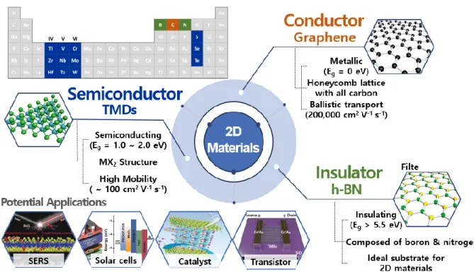
Introduction
The following chapters provide the background for the material property modulation via defect construction of TMDs for a better understanding of the thesis. In this chapter, the role and utilization of the chalcogen vacancy as doping agents will be introduced. The phase transition and the activation of the piezoelectric properties in the idle-induced TMDs induced the lateral growth of Li metal by increasing the Li-ion flux and increasing the binding energy of Li-ion and TMDs, effectively inhibiting dendritic growth of Li metal.
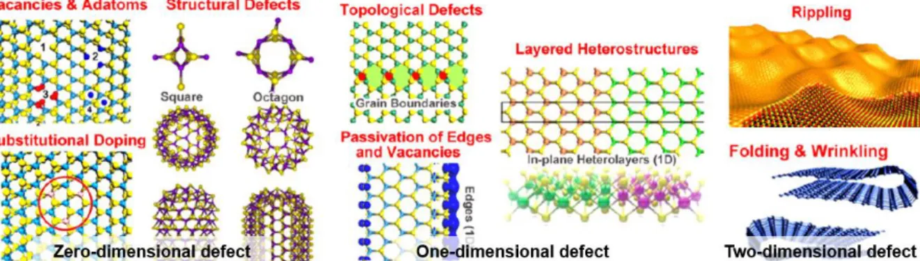
Defects in 2D Semiconductors: Classification, Generation, and Their Effects on the
- Classification of Defects
- Generation of Chalcogen Vacancy
- Effect of Chalcogen Vacancy on the Materials Properties of TMDs
- Effect of Chemical Doping on the Materials Properties of TMDs
- References
We specifically focus on the creation of a chalcogen vacancy in a chemical vapor deposition (CVD) approach. The most commonly adopted approaches to create a chalcogen vacancy in the TMD network are post-treatments of synthesized TMDs. In the case of electrochemical properties, the chalcogen vacancy was used to activate the inert basal plane of the TMD.
In Situ Coalesced Vacancies on MoSe 2 Mimicking Noble Metal: Unprecedented Tafel
Research background
Experimental details
Results and discussion
Conclusion
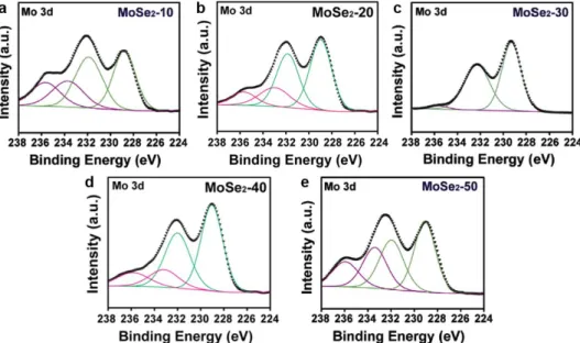
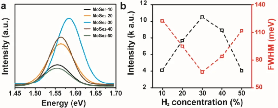
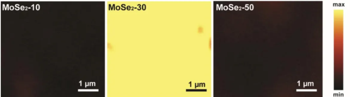
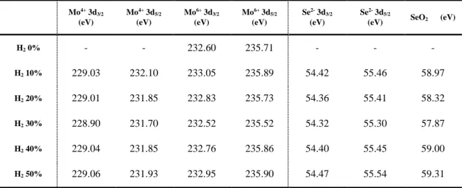
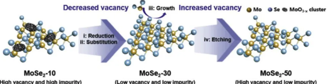
The atomic ratio (Se/Mo) of MoSe2 was calculated from the XPS spectra to quantify the concentration of Se vacancy in the MoSe2 lattice. To characterize the Se vacancy in the MoSe2 lattice, MoSe2-30 (low vacancy with negligible MoO3-x cluster) and MoSe2-50 (high vacancy with negligible MoO3-x cluster) samples were characterized by annular dark-field STEM with atomic resolution. (ADF-VOTE). Schematic diagram of lattice structure changes according to Se vacancy in MoSe2 lattice. a) ADF-STEM with atomic resolution and (b) corresponding atomic position assignment of stoichiometry MoSe2 (MoSe2-30).
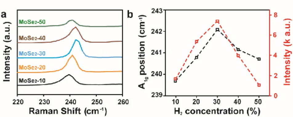
Such Se vacancies of Se atoms can be better visualized using the atomic position map (Figure 3.14b). a) Atomic resolution ADF-STEM and (b) corresponding atomic position mapping of non-stoichiometric MoSe2 (MoSe2-50). As the free space of Se decreased, the corresponding Mo 3d and Se 3d binding energies decreased gradually.33,35. a) Atomic resolution ADF-STEM and (b) corresponding atomic position mapping of non-stoichiometric MoSe2 (MoSe2-50). Compared to MoSe2-30, the observation of the shift in the Mo 3d and Se 3d peak positions for both higher and lower hydrogen concentrations confirmed the n-doping effect, induced by the Se vacancy in MoSe2.
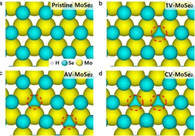
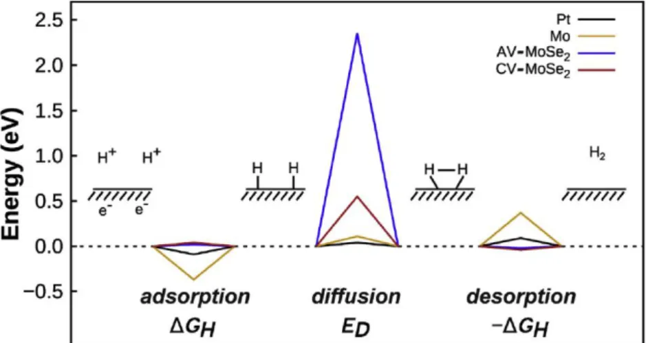
Se vacancy configurations, due to ΔGH is one of the good indicators of the HER activity.39. The Se vacancy configuration models (pristine MoSe2, 1V-MoSe2, AV-MoSe2 and CV-MoSe2) including H adsorption sites are described in Figure 3.20. This result confirms that Se vacancy in MoSe2 lattice can act as the determining factor for the Volmer reaction.
Furthermore, to better understand the origin of the Volmer reaction, we calculated the electronic band structures of MoSe2 according to the concentrations of Se vacancies (Figure 3.22). As the concentration of Se vacancies increased, localized electronic states (flat band) were created between the valence and conduction bands. Therefore, we believe that an additional Tafel reaction caused by Se vacancy formation induced high HER activity in vacancy-modulated MoSe2, which is schematically illustrated in Figure 3.24.
Research background
Experimental details
Results and discussion
Conclusion
The synthesized MoS2 film showed high uniformity, homogeneity, and scalability at 4-inch scale regardless of sulfur vacancy concentrations. Characterization: The surface morphology of the vacancy modulated MoS2 thin film was obtained via the cold FE-SEM (S-4800, Hitachi), OM (Eclipse LV150, Nikon) and dimension AFM (DI-3100, Veeco). As shown in the figure, it is observed that the crystallinity of the LV-MoS2 thin film increases as the crystallinity temperature increases.
The surface morphology of the synthesized vacancy-modulated MoS2(HC) was characterized by atomic force microscopy (AFM) and scanning electron microscopy (SEM) analysis. The chemical composition and crystallinity of the sulfur vacancy controlled MoS2 was carried out in detail. The atomic arrangement profile together with the sulfur atoms was investigated to confirm the effect of the sulfur vacancy introduction into the MoS2 lattice.
As the sulfur vacancy increased in its lattice, more donor states were formed. For the potential application of the vacancy-controlled MoS2, the electrochemical activity of the MoS2. The effect of the MoS2 crystallinity on the HER activity was first analyzed using LV-MoS2.
Furthermore, the HER activity of the sulfur vacancy-modulated MoS2 was analyzed using the optimized crystallinity (MoS2(HC)). A group VI transition metal dichalcogenides (TMDs), including molybdenum disulfides (MoS2), molybdenum diselenides (MoSe2), tungsten disulfides (WS2), and tungsten diselenides (WSe2) were one of the most explored 2D semiconductors. The effect of graphene integration process on the performance of graphene-based Schottky Junction solar cells.
Boosting the Photovoltaics Effect of 2D Heterojunction through the Chemical
Research background
Experimental details
Results and discussion
Conclusion
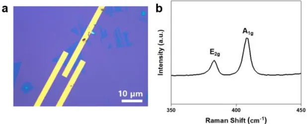
As shown in the optical microscopy (OM) image, a MoS2 flake with a triangular shape was successfully synthesized by a solution-phase CVD approach, as shown in Figure 5.1a. The corresponding Raman spectrum with sharp A1g and E2g peaks also confirmed that high-quality monolayer MoS2 was synthesized (Figure 5.1b).17 In the case of WSe2, ammonium tungsten oxide (ATO) and Se powder were used to synthesize WSe2 flakes. OM (Figure 5.2a) and Raman (Figure 5.2b) confirmed that high-quality WSe2 flakes were successfully synthesized by the liquid-phase CVD approach.18.
In the output characteristic in the WSe2 FET device, the decrease in Isd relative to the increase in Vbg indicated that the p-type characteristic of WSe2 was synthesized (Figure 5.5a). As shown in Figure 5.5b, the fabricated WSe2 device showed a dominant p-type ambipolar behavior. a) OM image of the MoS2/WSe2 heterostructure. The sharp Raman peak associated with MoS2 and WSe2 in the overlap region indicates the shape of the MoS2 and WSe2 heterostructure (Figure 5.6b).
In addition, the intensity of photoluminescence (PL) suppression in the overlapping region also confirmed the formation of the heterostructure (Figure 5.6c). Raman intensity mapping of MoS2 A1g (Figure 5.6d) and WSe2 A1g (Figure 5.6e) confirmed the uniformity of the synthesized MoS2/WSe2 heterostructure. The transmission characteristics in Figure 5.10 show the electrical properties of WSe2 doped with MoO3 and AuCl3.
As shown in Figure 5.11, although J-shaped curves were not observed in the MoS2/MoO3-doped WSe2 heterostructure, the current density was greatly increased.
Defect-Induced Piezoelctric 2D Semiconductors as the Host Materials for Stable
- Research background
- Experimental details
- Results and discussion
- Conclusion
- References
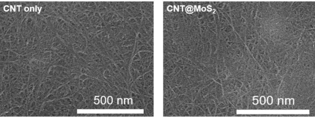
Characterization: The morphology of the CNT@MoS2 composite anode and the deposited Li-metal film was obtained by FE-SEM (Hitachi, S-4800). As shown in the electrochemical activity in Figure 6.5, the stability of the Li-metal anode strongly depended on the type of electrolyte. After that, to confirm the deposition of Li-metal on the CNT@MoS2 anode, the morphology of Li-metal was analyzed using SEM analysis as shown in Figure 6.6.
At PC and DOL, observation of some stripping areas in the Li metal surface showed the non-uniform Li metal deposition on the CNT@MoS2 anode. However, by linear ether including TEGDME and DEGDME, the Li metal was uniformly deposited on the CNT@MoS2 composite membrane. Therefore, in our work we use TEGDME as the electrolyte to characterize the CNT@MoS2 composite membrane for Li-metal batteries.
SEM images of Li metal anode of CNT@MoS2 after the lithium plating according to electrolytes. As shown by the electrochemical performance, the MoS2 coated CNT composite anode showed stable deposition of Li metal, as shown in Figure 6.8. The uniform deposition of Li metal is mainly attributed to the phase transition of MoS2.
The piezoelectric MoS2 could attract the Li ion more strongly, leading to effective suppression of the dendritic growth of the Li metal anode.
Summary
돌이켜보면 제가 무사히 학위를 마칠 수 있었던 것은 학위과정 동안 크고 작은 많은 분들의 도움이 있었기 때문입니다. 과학과 연구에 관심이 많았던 나에게 UNIST 진학은 진로를 결정하는데 가장 큰 도움이 됐다. 당시 제가 부족했던 물질적, 정신적 지원과 제가 올바른 길로 나아갈 수 있도록 지도해주신 덕분에 제가 하고 싶었던 연구를 하면서 성공적으로 학위를 마칠 수 있었습니다.
지난 7년, 짧을 수도 있고 길 수도 있는 시간 동안 저에게 베풀어주신 은혜에 대해 교수님께 감사의 말씀을 전하고 싶습니다. 사회에 나가서도 교수님의 명예에 훼손이 되지 않도록 늘 발전하는 학생이 되도록 노력하겠습니다. 부족한 점이 많았음에도 불구하고 저를 믿어주시고 선배님들이셨던 연구실 동료분들께 다시 한 번 진심으로 감사드립니다.
마지막으로, 해외 생활에도 불구하고 항상 저를 믿고 아무것도 걱정하지 않고 공부에 집중할 수 있도록 도와주신 아버지, 어머니, 동생 종민님께 감사하다는 말씀 전하고 싶습니다. 많은 분들의 도움 덕분에 긴 대학원생활을 무사히 마칠 수 있었습니다. 사회에 나가면 많은 도움을 주신 분들께 부끄럽지 않은 사람으로 살아가도록 노력하겠습니다.
마지막으로 도움을 주신 분들께 감사의 말씀을 전하고 싶습니다.