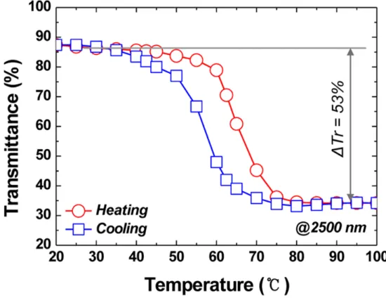
In Part 2, we report on the highly efficient hydrogen gas sensor based on the metal-to-insulator transition (MIT) of the electrothermally induced palladium nanoparticle-decorated VO2 nanowire fabricated by the efficient and size-controllable growth method originating from V2O5 thin film driven. We have many experiments for improved hydrogen gas detector based on MIT. When exposed to trace amounts of hydrogen gas in a single nanowire configuration, the enhanced conductivity gave rise to about twice as fast transition to the metallic phase even near room temperature (~35°C), reaching much faster (~3x) a critical current density , at which self-heating starts. Finally, especially the Palladium-VO2 nanowire near-corshell nanostructure shows remarkably large current increase at a temperature 10 °C lower than the bulk MIT temperature.
This current increase occurs slowly over several seconds to several tens of seconds, depending on the Pd coverage, temperature and hydrogen concentration. This information is available free of charge via the Internet at http://pubs.acs.org--- 43 Figure 3.16 (a) Low magnification SEM image of VO2 nanowires, (b) low magnification TEM images and (c) High magnification TEM images of a single VO2 nanowire, (d) SEM image of a single nanowire spanning gold contacts separated by approximately 15 μm.
INTRODUCTION
- CHARACTERISTIC OF VO 2
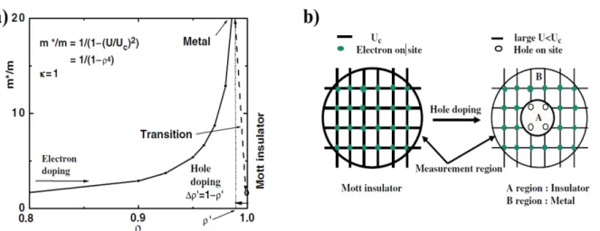
- MOTT TRANSITION
- GROWTH METHODES OF VO 2 NANOWIRES
- SPONTANEOUS CONVERSION OF V 2 O 5 THIN FILM INTO VO 2 NANOWIRES
- INTERNAL-STRAIN CREATED BY HYDROGEN GAS IN Pd-VO2 NEAR COR-SHELL AND
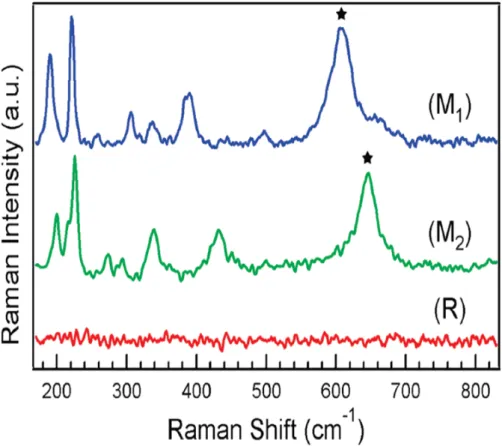
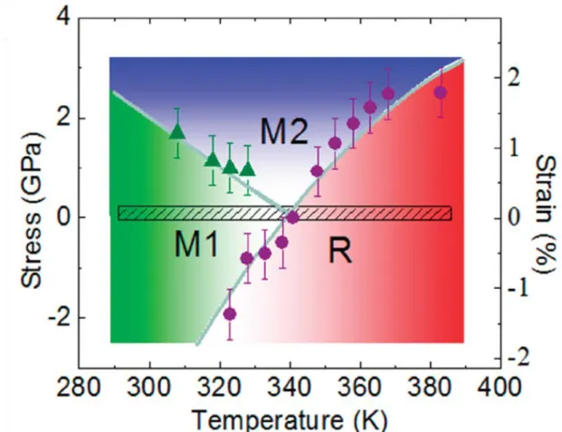
Raman spectra.[15] Raman spectra were measured by heating the vanadium dioxide nanowire. Figure 1.3[15] shows the insulating phase M1 and M2 and the metallic phase R of the Raman spectrum peak. The Raman spectra changed from 608 cm-1 (M1 phase) to 645 cm-1 (M2 phase) of the broad peak, increasing the temperature, and then the entire peak of the Raman spectrum disappeared, changing the metallic phase of vanadium dioxide . We suggest that VO2 nanowires with extremely narrow size and length distributions can be successfully grown on many substrates through the complete denaturation process from the V2O5 phase thin film.
We also report an unusual insulator to metal transition of the palladium-decorated VO2 nanowires caused by the heterogeneous H2-Pd catalytic reactions. These experiments allow us to investigate the deceleration in the transition with respect to the catalytic reactions in detail.
EXPERIMENT
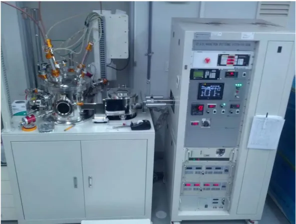
- Experimental Equipment of VO 2 nanowire growth
- Target and Substrates
- Analysis
- Experimental methods
To grow the nanowire of VO2, we used an atmospheric pressure and physical vapor deposition (APPVD). We may be able to flow three gases (He, H2, N2) in a 1 inch horizontal quartz tube furnace. After the growth of VO2 nanowires, VO2 nanowires were confirmed by Raman spectroscopy, which is the method to analyze VO2 in comparison with other composites.
When measuring the VO2 nanowire, to avoid deformation or damage of a VO2 nanowire by laser-induced heating, we kept the laser power at 0.15 mW. The crystallinity of VO2 nanowires was confirmed using a high-resolution X-ray diffractometer (Bruker, D8 Advance, Germany), which is equipped with a dual-channel asymmetrically cut monochromator on a motorized slide. To observe the morphology of the VO2 nanowire, Field Emission Scanning Electron Microscopy (FE-SEM) was performed using a Nano 230 from FEI that contains a Schottky-type thermal field emission gun and provides a microscope resolution of 1.0 nm at 15 kV, a magnification range of x.
High-resolution transmission electron microscopy (HRTEM) images were performed using a Cs-corrected JEOL JEM-2100F TEM operating at 200keV. Then, the fabricated thin films were moved into the middle of a horizontal 1-inch quartz tube furnace to grow VO2 nanowires under atmospheric pressure. High-resolution transmission electron microscopy (HRTEM) images were collected using a Cs-corrected JEM-2100 operating at 200keV.
The microstructure of VO2 nanowires was verified by X-ray diffraction (XRD) and Raman spectroscopy. Electrical contacts were deposited on individual VO2 nanowires on SiO2/Si growth substrates. Au/Ti (200/20 nm) electrodes were fabricated by conventional e-beam metal vapor deposition through a metal shadow mask.
RESULTS AND DISCUSSION
- V 2 O 5 thin film fabrication
- VO 2 nanowire growth with V 2 O 5 thin film thickness
- Micro-structure analysis of grown VO 2 nanowire
- Grown VO 2 nanowires with substrates
- Annealing conditions of metal contact
- Calculation of Insulator-to-Metal Transition temperature
- Guided growth of sub-millimeter long VO 2 nanowires
- VO 2 nanowire morphology control with patterned-substrate shapes
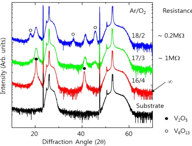
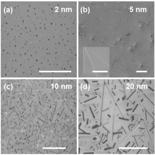
The corresponding SEM image shows VO2 nanowires grown on SiO2 substrates with different thicknesses of V2O5 thin films from 2 to 20 nm (Figure 2.6). VO2 nanowires were grown on a SiO2/Si substrate that is lower than the main cure. Only the diffraction peaks of the (011) and (022) planes are shown, indicating that the VO2 nanowires synthesize the preferential direction.
Excited by 533 nm laser light, the Raman spectra of single nanowires are observed (Figure 2.7b). VO2 nanowires were grown on a sapphire (Al2O3 c-plane) substrate. To show the Raman spectra, we kept the laser power at 0.15 mW and had 300 seconds of exposure time, because the VO2 nanowires are easily deformed and burned by laser-induced heating. On an unpolished SiO2/Si substrate, the VO2 nanowires have random angles from a floor (Figure 2.8b).
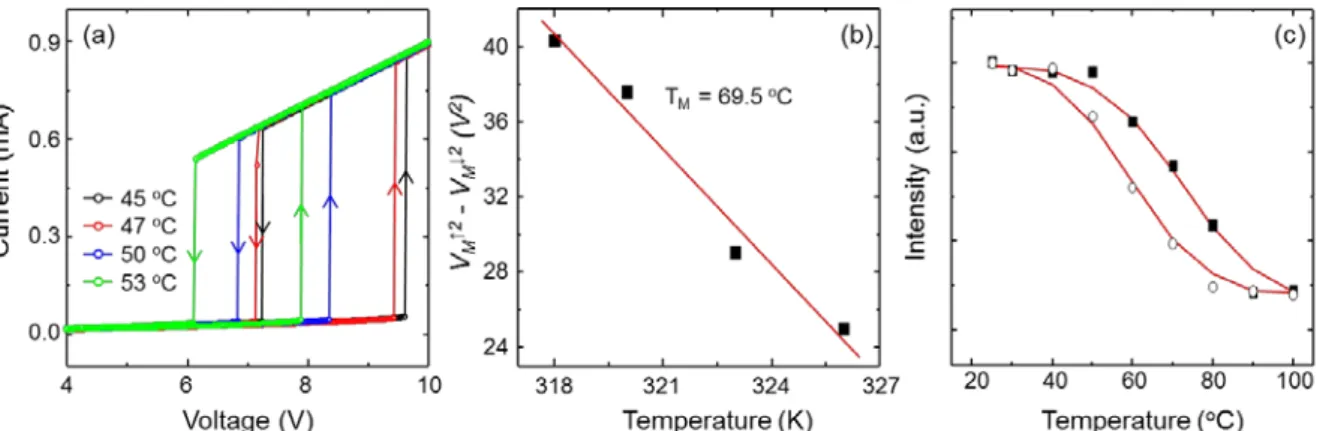
The values of TM determined in the above manner as a function are shown in Figure 2.10. Raman spectra of VO2 were observed to measure the transition temperature from insulator to metal. We have observed aligned, submillimeter growth of VO2 nanowires with controlled morphology.
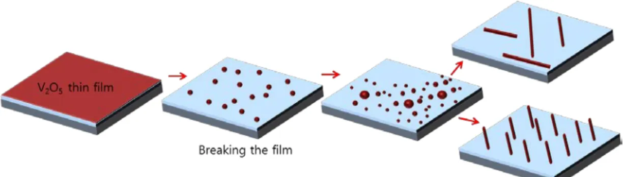
By changing the slope of the substrate patterns, we showed that liquid V2O5 nanodroplets coalesce into larger droplets and that large droplets transform into VO2 nanowires. On patterned substrate, the cross-sectional shapes of VO2 nanowires are determined by the shapes of cups. The cross-sectional shapes of VO2 nanowires are determined by the cup shapes as the solid V2O5 thin films melt into liquid V2O5 nanodroplets.
CONCLUSIONS
INTERNAL-STRAIN CREATED BY HYDROGEN GAS IN Pd-VO2 NEAR COR-SHELL AND
EXPERIMENT
- EXPERIMENT
- Experimental equipment
- Analysis
- Experimental methods
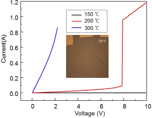
In Figure 3.10 (b), the hydrogen current until before e-beam irradiation causes the current to rise very slowly, and then the rate of the current increases significantly after ~7 min of H2. The change in the response time of Pd-decorated VO2 nanowires with e-beam irradiation is summarized in Figure 3.10 (c). Interestingly, the response time dropped drastically to less than 10 seconds as the Pd thickness increased to 2.5 nm. This reduction in response time due to the increase in conductivity could be observed near room temperature (35 ~ 40 °C), as shown in Figure 3.11.
The actual average temperature of the nanowire can be accurately measured using the resistance of the nanowire itself, as the temperature was varied from 303 K to 323 K in the presence of hydrogen (Figure 3.13). As the hydrogen concentration decreases, the rate at which the current increases becomes slow and the response time decreases exponentially with H2 concentration (Figure 3.18b). To see the influence of Pd coverage on the current response, we analyzed a quantitative relationship between the distance between Pd nanoparticles, and the response time was plotted with the H2 concentration of 500 and 5000 ppm (Figure 3.19). As shown in Figure 3.17 (a), when the Pd nanoparticles are well dispersed and the distance between the Pd nanoparticles is very short (< 3 nm), the transition occurs within 1-2 s.
At low Pd coverage, the increase in carrier density with hydrogen exposure time is initially observed as a constant conductance increase of the nanowire while in its insulator phase in Figure 3.17 (a). Here, in the region with a bare surface, the temperature changes linearly, but it shows a quadratic change in the region covered by a Pd particle, as shown in Figure 3.21 (a). As shown in Figure 3.21 (b), the global temperature profiles are almost the same, although there is a slight deviation locally.
We calculated the changes of temperature, compressive stress and conductivity of VO2 nanowire by changing the length of VO2 nanowire from 24 μm to 198 μm, as shown in Figure 3.20 (b). The profiles of temperature and the corresponding electrical conductivity at t = 20 sec. is shown in Figure 2.21 in the Supporting Information. In the profiles of temperature and electrical conductivity at t = 20 sec (Figure 3.21), as the coverage increases, the maximum temperature increases, consistent with the results in Figure 3.19.
RESUITS AND DISCUSSION
- VO 2 nanowires doped by tungsten
- Analysis of VO 2 nanowires doped by tungsten
- Current-density change with e-beam irradiation conditions
- Crystal structure analysis of VO 2 nanowires following e-beam irradiation
- Mott transition temperatures with e-beam irradiations; I-V measurement
- Mott transition temperatures with e-beam irradiations; Raman Spectra
- Sensing performance with e-beam irradiation conditions
- Detecting hydrogen gas at the room temperature
- The selectivity of different four gases
- The temperature coefficient of resistance
- VO 2 nanowire temperature calculation by COMSOL multiphysics package
- Induced defects from high e-beam energy
- SEM & TEM images of palladium deposited & non-deposited VO2 nanowires
- Response rate with palladium thickness
- Response rate with hydrogen concentration
- Response rate with palladium distance
- Phase transition in VO 2 due to localized heating via Pd-H reaction
- Two recovery methods following hydrogen flow
- Sensing performance at the low voltage and room temperature
CONCLUSIONS
In summary, we showed that increasing the conductivity was one of the effective methods to accelerate the response and reduce the operating temperature of an MIT-based hydrogen sensor. Irradiating a well-controlled electron beam into the nanowires significantly increases the conductivity of nanowires up to 4 times with little change in the insulator to metal transition temperature (< 2 °C). The conductivity is further increased when exposed to trace amounts of hydrogen gas, which causes the insulator to transition to a metal after a few minutes.
As the conductivity increases, the transition to metallic phase can occur faster (~ 2 x) even near room temperature (~ 35 °C), by reaching faster (~ 3 x) a critical current density at which the self-heating starts. The self-heating effect accelerated by the increase in conductivity leads to a decrease in response time, in the operating temperature and voltage. We also reported an unusual insulator-to-metal transition of the palladium-decorated VO2 nanowires induced by the heterogeneous H2-Pd catalytic reactions.
The Pd-VO2 showed a sudden increase in conductance from insulator to metal at a lower temperature (~ 50 °C) than 68 °C in the bulk upon hydrogen gas exposure. The sudden change occurred smoothly over a duration of several seconds to several tens of seconds, depending on the Pd coverage, temperature, and hydrogen concentration. Electronic transport measurements and finite element analyzes with various experimental conditions such as hydrogen concentration, temperature, Pd coverage and applied voltage indicate that the delay in the transition is due to the formation of alternating domains of metal and insulator regions of the VO2, which was produced by the heat generated by the exothermic catalytic process.
Although the nanoscale heating may be negligible in gas sensor materials such as ZnO and SnO2 etc., it is believed to be sufficient to initiate the transition along the nanowires at ambient temperature close to the insulator to the metal transition temperature in the bulk. After the hydrogen flow is turned off, the conductivity does not immediately return to the original value and it takes 30 min even after 100 °C, which means that the atomic hydrogens produced by dissociative chemisorption on Pd are incorporated into VO2. However, the Pd-decorated VO2 nanowire also shows a similar current response to hydrogen after the recovery process, meaning it is reversible.