DIRECT DIGITAL CONTROL OF PERMANENT MAGNET BLDC MOTOR
FOR AIR CONDITIONING
By
HARYATTIE BINTIAZIZI
FINAL YEAR PROJECT REPORT
Submitted to the Department of Electrical & Electronics Engineering in Partial Fulfillment ofthe Requirements
for the Degree
Bachelor ofEngineering (Hons) (Electrical & Electronics Engineering)
UniversitiTeknologi Petronas Bandar Seri Iskandar 31750 Tronoh
Perak Darul Ridzuan
© Copyright 2007 by
Haryattie binti Azizi, 2007
CERTIFICATION OF APPROVAL
DIRECT DIGITAL CONTROL OF PERMANENT MAGNET BLDC MOTOR FOR AIR CONDITIONING
Approved:
by
Haryattie binti Azizi
A project dissertation submitted to the Electrical & Electronics Engineering Programme
Universiti Teknologi PETRONAS in partial fulfilment ofthe requirement for the
Bachelor ofEngineering (Hons) (Electrical & Electronics Engineering)
etc
Dr. K. S. Rama Rao
Project Supervisor
UNIVERSITI TEKNOLOGI PETRONAS TRONOH, PERAK
June 2007
i n
CERTIFICATION OF ORIGINALITY
This is to certify that I am responsible for the work submitted in this project, mat the
original work is my own except as specified in the references and acknowledgements, and that the original work contained herein have not been undertaken or done by
unspecified sources or persons.
>4--
Haryattie binti Azizi
ACKNOWLEDGEMENTS
Firstly, I would like to express my gratitude to Allah S.W.T for His grace to enable completion of the final year project. With strength and knowledge that blessed by Him, I was able to carry out and accomplish.
My heartfelt thank goes too my supervisor, Dr. K.S. Rama Rao for his guidance and patience that lead to accomplishment of this project. Under his supervision, I encountered a lot of new things. Thanks to him, the project is very resourceful and easy to understand. His sharing of knowledge, kindness and patience will always be appreciated.
Next, thanks to my family and friends for willingly to understand my needs in the making of the projects. From the bottom of my heart, I would like to thank them for being very supportive and sharing word ofwisdom together.
Not to forget Vivian Huyen from Lin Engineering who always being helpful during my projects. Thanks to her, I understand better the concept of BLDC motor.
Lastly to all lecturers, staffs and students whose names are not mentioned here but actively being helpful with guidance, directly or indirectly, thanks a lot. Without the help that I got from everyone, this project would be a failure. Thank You.
ABSTRACT
This is a design project which to design a direct digital control of permanent magnet BLDC motor for air conditioning. Mainly the task of this to developed a control to the speed of BLDC motor that will determine the speed of compressor inside in an air- conditioner. The project is divided into two main tasks; the simulation part and circuitry part. This report will delivered results, discussion and feedbacks of the both parts that had been handled. The simulation is build inside MATLAB/SIMULINK while the circuitry part is built by using equipments of Lab-Volt. It composed from blocks that are mainly based on calculation or theoretical value. So it is completely logical blocks and shall not interface with other Power Electronic block set components inside MATLAB. From here the author learns relationship between Sensoriess BLDC motor and BLDC motor with Hall Sensor. In circuitry part, the IGBT inverter by supplying PWM control signals. From here the author learns that the output voltage depends on switching process and the DC input. Due to lots of advantages deliver by BLDC motor, this project brings a lot of benefit.
TABLE OF CONTENTS
CERTIFICATION ft
ABSTRACT vi
LIST OF TABLES ix
LIST OF FIGURES x
LIST OF ABBREVIATIONS xii
CHAPTER 1 INTRODUCTION 1
1.1 Background ofProject I
1.2 Problem Statement 1
1.3 Objectives , 2
1.4 Project Planning 2
CHAPTER 2 LITERATURE REVIEW AND THEORY 3
2.1 Brushless DC Motor 4
2.2 Simulation Tools .. 6
2.3 Pulse Width Modulation Inverter ..7
2.3.1 Operation of PWM Inverter 8
CHAPTER 3 METHODOLOGY 10
3.1 Flowchart 10
3.2 Tools 11
CHAPTER 4 RESULTS AND DISCUSSION 12
4.1 Simulation with Matlab/Simulink 12
4.1.1 The mybldc block.... 13
4.1.2 The estimation block 15
4.1.3 Zero crossing block 15
4.1.4 IC and 120 deg trigger blocks 17
4.1.5 The Controller block 18
4.1.6 The All Phase block 20
4.2 Results and Discussion of simulation 21
4.2.1 Stator phase currents ...21
4.2.2 Rotor speed 22
4.2.3 Voltage applied to BLDC motor 23
4.2.4 Back Electromotive Force 24
v n
4.2.5 Currents after controller.... 24
4.2.6 Zero crossing 25
4.3 Construct the digital controller and power circuits, , 26
4.3.1 Designing boost converter .„26
4.3.2 Experimental test on BLDC motor 28
4.3.3 Test BLDC motor without Hall Sensor feedback to the Lab-
Volt controller.. 30
4.3.4 Test BLDC motor while Hall Sensor are attached to the
designed controller.... 35
4.3.4.1 Designed controller hardware 36
4.3.5 Test BLDC motor with the designed controller 37
4.3.6 Correction to the controller 38
CHAPTER 5 CONCLUSION AND RECOMMENDATION 39
REFERENCES ..41
Appendix A Gantt Chart 42
Appendix B BLDC Motor Specification 43
Appendix C Results of Simulation 44
Appendix D coding for microcontroller 56
Appendix E Datasheets 59
LIST OF TABLES
Table 1 Design parameters 27
Table 2 Results oftest 35
IX
LIST OF FIGURES
Figure 1 BLDC drive system 3
Figure 2 BLDC motor 4
Figure 3 Torque-speed characteristic for BLDC motor 5
Figure 4 Stator of BLDC motor 5
Figure 5 Arrangement ofpermanent magnet in rotor ...6
Figure 6 PWM inverter with R-L load 7
Figure 7 Sine-triangle, pulse-width-modulated control waveforms, phase voltages
Vag and Vbg, and line voltage Vab 8
Figure 8 Flowchart ., ... ....10
Figure 9 Matlab software 11
Figure 10 Lab-Volt Power Electronics Equipment 11
Figure 11 BLDC motor simulator 12
Figure 12 mybldc block 13
Figure 13 Inside of mybldc block „.... 13
Figure 14 my state space parameters 14
Figure 15 S function parameters 14
Figure 16 Estimation block 15
Figure 17 Zero crossing block... ,. 15
Figure 18 Zero crossing detection for Back EMF phase U and phase V 16 Figure 19 Zero crossing detection for Back EMF phase V and phase W 16 Figure 20 Zero crossing detection for Back EMF phase U and phase W 17
Figure 21IC block 17
Figure 22 120 deg trigger block 17
Figure 23 Sub block of IC 18
Figure 24 Controller block 18
Figure 25 Reference structure of Inverter „ 19
Figure 26 Sub system of controller block 19
Figure 27 AHPhase Block 20
Figure 28 Output of voltage at phase U 20
Figure 31 Voltageapplied to Phase U, V and W 23
Figure 32 BackEMF for Phase U,Vand W 24
Figure 33 Current generatedafter controller to Phase U, V and W 25
Figure 34 Zero crossingto Phase U, V and W 26
Figure 35 Boost converter topology 27
Figure 36 The switch and diode current ...» 27
Figure 37 Experimental setup , 29
Figure 38 Lab-Volt control unit and inverter., 29
Figure 39 Test BLDC motor withoutHall Sensor feedbackto controller 30
Figure 40 Chopper/Inverter control unit 31
Figure 41 At 20% duty cycle 31
Figure 42 At 30% duty cycle 32
Figure 43 At 40% duty cycle 32
Figure 44 At 50% duty cycle 33
Figure 45 At 60% duty cycle 33
Figure 46 At 80% duty cycle 34
Figure 47 At 100% duty cycle 34
Figure 48 Test BLDC motor while Hall Sensorare attached to designedcontroller. 35
Figure 49 Circuit diagram-parti 36
Figure 50 Circuit diagram-part2 37
Figure 51 Test BLDC motorwith designed controller alone 38
Figure 52 The correction of controller circuit 38
XI
LIST OF ABBREVIATIONS
DDC - Direct Digital Control AC - Alternating Current
DC-Direct Current
BLDC motor - Brushless DC Motor PWM - Pulse Width Modulation EMF - Electromotive Force L- Inductor
C- Capacitor
CHAPTER 1 INTRODUCTION
1.1 Background of Project
BLDC abbreviation for Brushless DC motor had been widely used due to its advantages. In air conditioning, BLDC motor had been used in compressor to enable the compressor to startat high revolution speed as soon the air conditioning system is turned on. [1] This project mainly focused on the application of BLDC motor for compact and small car air conditioner.
The drive system, use Direct Digital Control or DDC as electronic control interface for BLDC motor. Under DDC, microcontroller is implemented. This system had contributed to hybrid vehicle such as Toyota's new Prius, Toyota Harrier Hybrid and Toyota Kluger Hybrid. This system had many advantages over universal DC motor or brushed DC motor as stated under "Permanent Magnet Brushless DC motors for Consumer Products". [2]
1.2 Problem Statement
Originally, the most common brushed motor had been widely used in many facilities such as in vacuum cleaners and washing machines as the manufacturing cost being quite low. However, many flaw arise such as relatively inefficient and having high
acoustic noise emissions. The BLDC motor had offers with potential of increasing the efficiency and reliability.
Basically the purpose of this project is to control the speed of a BLDC motor for a car
air conditioner.
1.3 Objectives
The objectives of this project are as follow:
• To develop a digital controller to control the speed of BLDC motor for a car
air conditioner
• To designthe control circuit, power circuitto operate the BLDC motor from a
battery source
• To model and simulate design with MATLAB/SIMULINK
• To construct the digital controller and power circuits
1.4 Project Planning
Duringthis semester, it is proposed to design and constructthe controller for BLDC motor. The process also involves simulation of the drive system using MATLAB/SIMULINK. Also it is proposed to implement the microcontroller for
CHAPTER 2
LITERATURE REVIEW AND THEORY
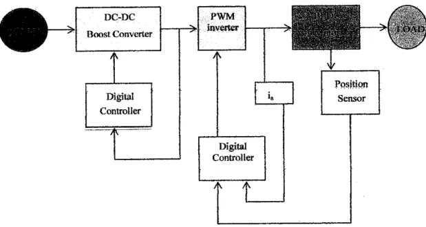
In continuation of preliminary report submitted in the first semester, the following chapters explain the project objectives of the second semester. Figure 1 show the
BLDC drive system.
DC-DC
Boost Converter
A
Digital
Controller
> r
Figure 1 BLDC drive system
PWM inverter
Digital
Controller
A A
Position Sensor
-> ii
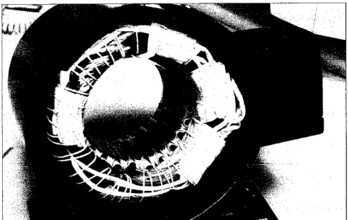
2.1 Brushless DC Motor
Figure 2 BLDC motor
The irrformation provided by a vendor for a Brushless DC motor with integral Electronics as shown in Figure 2 published [3j that it is typical for scientific applications (stirring equipment pumps, mixing machine) and industrial applications (fans and conveyor). The motor itself is already equipped with internal drive electronics that provides control, There are two main components inside the motor;
internal speed regulation and electronic commutation. The full specification of the motor are listed mthe Appendix.
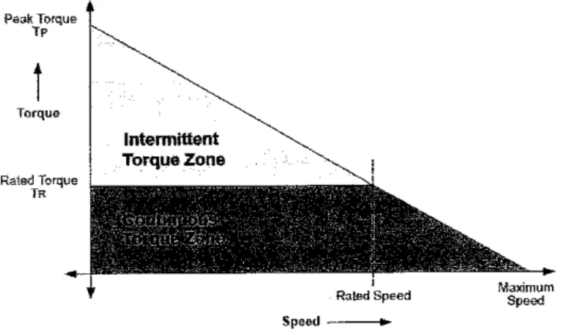
Generally the motor's speed can be controlled by changing the terminal voltage. As
Speed
Figure 3 Torque-speed characteristic for BLDC motor.
A BLDC motor is a type of synchronous motor. As usual it consists of two main parts- stator and rotor. The stator, it consists of piled steel laminations with windings placed in the slots that are axially cut along the inner periphery. [7]
Figure 4 Stator of BLDC motor.
The rotor, it is made from permanent magnets that can vary from two to eight pole pairs with alternate North (N) and South (S) poles. [7]. Figure 5 show the arrangement of permanent magnets in rotor.
Circular core with magnets oil tfie periphery
Circular core with rectangular rnagfiets emisedded in the rotor
Circular core with rectangular magnet!
inserted intotliB-rotor core
Figure 5 Arrangement of permanent magnet in rotor.
2.2 Simulation Tools
As explained earlier, the main simulation tools that will be used are PSPICE and Matlab/Simulink. The project will be concentrated on first part; the simulation.
Matlab/Simulink is the most suitable simulation tools for an electromechanical system. It is essential to develop the simulation model.
2.3 Pulse Width Modulation Inverter
Ta+ Xi Da+ Tb+ \ i Db+ /* u+ \ i Dc
Vdc a i i
a a
c • •
VcCll
T„-V A Oa_ Th-\ ? Db- c - £e-
a s v « C s
Figure 6 PWM inverter with R-L load
A PWM inverter as shown in Figure 6 is a part of the BLDC drive system. The purpose of inverter itself is simply to invert DC to AC. The objective of using specifically PWM inverter is to shape and control the three-phase output voltages in magnitude and frequency with respect to the DC input voltage. The stator of the motor is represented by the three phase loads. The input source voltage to inverter is DC voltage, VDC- The output will be displaced by 120° with respect to each other.
The output voltage for eachleg (Vag, Vbg, Vcg) depends on the input voltage, Vdc and the switch status and independent ofthe output current. It also means that the output voltage is independent of direction of the load current.
2.3.1 Operation ofPWMInverter
The inverter is fed by a dc voltage and has three phase-legs each consisting of two transistors and two diodes (labeled with subscripts a, b, c). With Sine-Triangle Pulse Width Modulated (STPWM) control, the switches of the inverter are controlled based on a comparison of the sinusoidal control signal and a triangular switching signal. The sinusoidal control waveform establishes the desired fundamental frequency of the inverter output, while the triangular waveform establishes the switching frequency of the inverter. The ratio between the frequencies of the triangle wave and the sinusoid is referred to as the modulation frequency ratio. The switches of the phase legs are controlled based on the following comparison [10]:
vcontrol(phase -a) > vtriangle >•* a + IS on vcontrol(phase-a) <vtriangle* *a- 1S on
vcontrol(phase-b) > ^triangle* ™b+ 1S on
vconirol(phase-b) <vtriangle> *b- *s on vcontrol (phase ~c)> vtriangle> *c + '1S on vco7itrol{phase - c) < vtriangle ? J c- •1S on
Vljiaad*
VUc
As shown in Figure 7, when the comparison is made, the output voltage range varies from the input voltage value and zero. For the line voltage, the dc components will
cancel out. Thus the range will be from +Vdc to -Vdc-
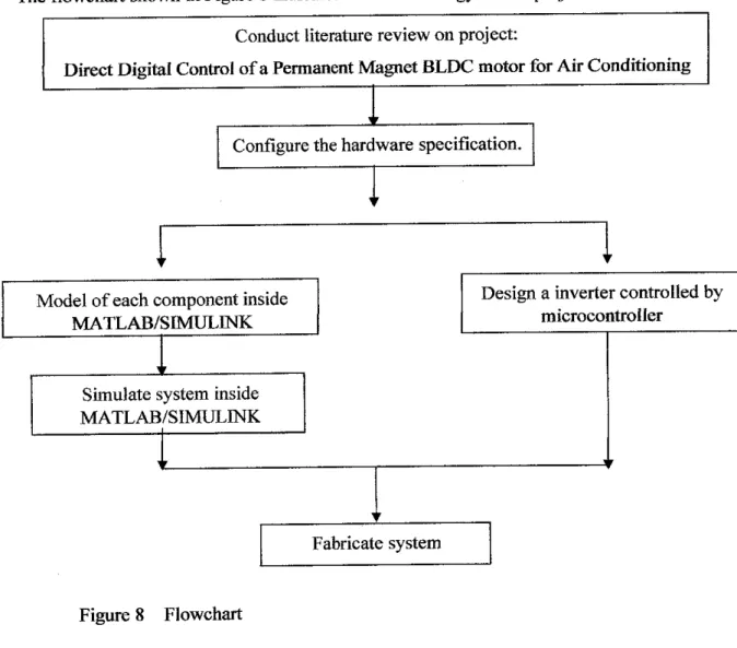
3.1 Flowchart
CHAPTER 3 METHODOLOGY
The flowchart shown in Figure 8 indicates the methodology of this project.
Conduct literature review on project:
Direct Digital Control of a Permanent Magnet BLDC motor forAirConditioning
Configure the hardware specification.
Model of each component inside
MATLAB/SIMULINK
Simulate system inside
MATLAB/SIMULINK
Figure 8 Flowchart
Fabricate system
Design a inverter controlled by
microcontroller
3.2 Tools
The following tools are used for software and hardware requirements ofthe project:
- Matlab/Simulink
- Lab-Volt Power Electronics Equipment
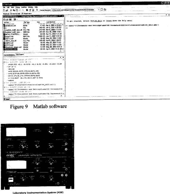
The simulation is conducted using Matlab/Simulink. The results of the simulation are discussed in Chapter 4 where the usage of this software is optimized. Most of the circuits for this project are built in the Power Electronics laboratory using the Lab-Volt Power Electronics Equipment. The prototype circuit is built from the available modules in the laboratory and the motor purchased from vendors.
FfeE* *** M*Jg Detftw Vfnkm mb
afffllteHTWrE™MftrtalfrPOiJCtrtn**nr ^ O [?D
m&Si a -
-t>._-t-_•-...-.-»* - r - l ^ THA.TI.ABK=lD K IISlrOH iTCra Eh* Help DCUIJ.
» dffftuec^OfleuBenCff ana aecclfiflBVuserVHT Oocownis\£yp\Bi.DC\if3jnuI«aE\ra9fciae_Mdl2.Hl
1
AiFfes- FtaTvuc Stn LMlkbUhfd
SmVbIDCZM Mfda 17KB (1)1.4.2001 ililHJi- 2C fi|E 146KB Jai5.2007.1.25531 iiiinj|plite radD stun.* DLLFflt 213XB Nov9.2CC6 1:11:18 te!]mifcbfc mfl3 b«hi... «E(«o 331 KB Doc 26.3006 1255-:
KNEW CONTROL!.. MoOeiI BitO ftir!i.a»J LOME SiBsuHmal MAT-Glo 9318KH Jm 11.20073.3132 BsETLmill Model 16 KB May25.3304 11401 ; 21SEN sHin.dll DLLFla 156KB UmB,2006 2:20-30 ; BSEnlmH Model 16KB May25.20U11:5D .{
HSEiainin MrnJil 16KB M>y25.3004 I1:«:: 1 HthfflstioU rtwle.rotf Mffltol 12KB Mjy20.3»* W-2 •
gpil.WlrilllTa Model HkB Aj>rB.20M1H1:4Bvj
'3
UntMW 'WntsntoB.
- J - !—l
n-O.025(0.35-0.075-0.05-O.DS]
- n=0.325*10.35-0.07S-0.05*0.G5) -b—D. 1H -0.1 *0. 075-0.05*O. DZ5>
c--0.025-E0.1»a-E&-D.35'-0.n25)
opcuCCi^DDCuiceiicfl am! 3rtsj 1fiS\<13et\Bj 0ocmnebiLa^i*v
Figure 9 Matlab software
Laboratory Instrumentation System (438)
Figure 10 Lab-Volt Power Electronics Equipment
11
CHAPTER 4
RESULTS AND DISCUSSION
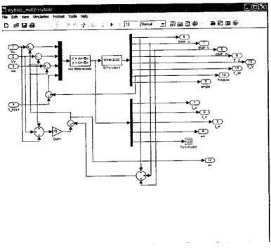
4.1 Simulation with Matlab/Simulink
The main task of simulation is to handle the model and run it with the specified design requirements. Initially the simulation is run for the inverter and BLDC motor
parts. The converter part is then simulated separately. Following is the explanation of
each block that is used for the simulation. The blocks are:
• mybldc block • 120deg trigger block
• estimation block • Controller block
• zero crossing block * AH phase block
• IC block
F*e e*t lfa-f &njfett*i Ferret TwfeHefci O e?
Figure 11 BLDC motor simulator
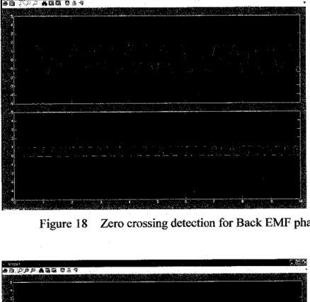
4.1.1 The mybldc block
U
«! l_v
L'
ty wjte
&&J1
=UFV
i s SMFW
T-U T_V TW Mac
Fic&n
Figure 12 mybldc block
This block act as a BLDC motor, where it will take inputs of three-phase voltage and
load torque values. This block consists of two sub blocks; my state-space and S
function. The state space model is developed from the mathematical modelrepresenting the motor equations.
n» Ecft ee*smiife: Fnnrat "in* h*
Figure 13 Inside of mybldc block
13
State-space niodet dx/dt=Ai*Bu
• yaQODu PaiamelEis
&
i 0-1.6aa?68e^-1.iei1^e*OI3ia-a3fl63ae^5~245245^OO;0OD2lli]
^(236.36 0OC;O2363BG0;PD23S.aEQ;O00 ^OflftOOOD]
i)1QOO0:01oao.-0010G;Q3D1Dp flo 01]
']0eOO:OO 00; 0 0 0 0.0000:00001 irtitBlcondEions:
*bsotieloteiance_
HE"" "
Figure 14 my state space parameters
S-Funcllan (maskt
The ttovfc post- ptccssd Ihe sfate hmcc btodt ou^ub Paiameter;
Muntei BSEurspei phase
Re&s!*icepg phase
jaTa^T"""
mmudjhductace petphase
41%U
O02^
vduc nf viscous fciaion 0.DD2
OTorrertof r&rfia
Tola! nurtiBi oJ&ole*
Sattrg vaiie of cudoftb friction 02^003
5faScMeJJon
Figure 15 S function parameters
If the models of the BLDC motor changes, the armature resistance and inductance will need to change. However due to lack of information, the changes will be made on resistance only. This are the outputs that produce from mybldc block:
• I_u, I v, I w are the individual phase currents
• wn is the rotor electrical speed in rad/s
• angle is the rotor electrical position as compared to the initial position
• EMF_U,EMF V,EMF_Ware the back emf values generated in the three phases.
• T_U,T_V,T_W ate the individual phase torques.
• Friction: the values of the friction faced by the rotor. Contains both static and
coulomb friction.
• vn is the neutral point node voltage.
4.1.2 The estimation block
Figure 16 Estimation block
This block calculates the error between the actual and command speed. The input to this block is taken from the mybldc block and error gen block. The inputs will be the actual value of the motor speed, rotor shaft position, the required rotor speed and lastly the fed back from the output. From this block the outputs such as command phase currents, error between command speed and actual speed and value oftorque to
be generated are observed.
This block can be considered to be inside the BLDC motor itself in real world and
cooperates with the next block to perform the Hall Sensor part ofthe motor.
4.1.3 Zero crossing block
i*o - o
fV fV
?ins Wsvs?
Stcpa
•
o
Ps
Figure 17 Zero crossing block
15
This block performs the translation of Hall Sensor inside the BLDC motor. The input parameters to this block are the back EMF for all the three phases from the motor.
Then the zero crossing will translate the input into 1 and 0 output only. The inputs and output of all three phases are shown in Figure 18 to 20.
Figure 18 Zero crossing detection for Back EMF phase U and phase V
Figure 19 Zero crossing detection for Back EMF phase V and phaseW
Figure 20 Zero crossing detection for Back EMF phase U and phase W
4.1.4 IC and 120 deg trigger blocks
;lUsst ) IV
u v
w u THREEHCtD
IC
Figure 21 IC block
0
V
w
120 deg bigger
Figure 22 120 deg trigger block
According to the author [9], the TC block is used to hold the controller to its initial state till the time motor picks up sufficient speed and the back EMF voltages are significant. This system however resembles the sensorless BLDC. But it still would
17
be significant for the use of the present work. Inside the IC block, there are a number of switches to select the output. These switches will be changing with the threshold
time that had been set.
Ffe EcH Hew SmufoSon Foimal Toob Help
d ia; a a -• -• -*. - *
d >
lUstar
IVsUl
iWslB-
a y .
G >
C!>
THHESK3LD
3 B 3E
= sSnilstiE
5v]
SnteiiT
SB®
< D
-*CE>
lYoui
*cn
-KZ3
-»CD
-KD
WJoul
Figure 23 Sub block of IC
Next would be the 120 deg trigger block which will give initial value to the system to ramp up the motor for a threshold time. Then it will disconnect the 120 deg trigger block from the system to perform the closed loop operation.
4.1.5 The Controller block
\UJr. Trt
lUSTARjr. Ti2
IV_E Tr3
ITOTARjr- Tnf
rw TiS
LWSTARJn Ti6
COMT ROLLER_MOD
Figure 24 Controller block
The controller block takes the output of the IC block and triggers the appropriate
gates of inverter. This system will work as inverter to supply the input voltages to the
04 Qs 02
jS±S
EACK-LWSIGNALSFigure 25 Reference structure of Inverter
CI.DC MOTOR
The sub system ofthe controller block can be viewed in Figure 26:
a >
lUSTARil
<z>
<T>
(^>
IWSTAR i
%
-KZ3
Tig
•*CZ3
Tr2
Figure 26 Sub system of controller block
19
4.1.6 The All Phase block
•t
QAT=I
HATH I
SATEJ !
«AIS* I
S&T£5 !
SAT3)|<
I
JLT
Figure 27 All Phase Block
This block takes input from the controller which is meant for the gates of the inverter.
The output voltage at Phase U is observed. The results can be seen below. Due to constant value in Gate 4, the phase voltage will take the positive terminal of the
voltage source.
pjZijD ft s •*?
Figure 28 Output of voltage at phase U
4.2 Results and Discussion of simulation
The simulation is iniated with a specific the amount of DC input voltage to the inverter. In this simulation it is assumed that the output from the converter is ideal and without any losses. The specified amount that been change in the model are the excitation voltage, resistance per phase, inductance per phaseand speed reference.
4.2.1 Stator phase currents
Figure 29 show the result of simulation of stator phase currents. This stator currents support the equation given where its will pass through resistance and inductance.
These currents are also proportional to the torque load on the motor shaft.
V,=IR + pLI + BEMF (l)
Torque = KtxI (2)
Vt= Voltage applied to motor per phase 1= Stator currents per phase
p = d/dt
L = Inductance per phase R = Resistance per phase BEMF = back EMF per phase
21
Instantaneous omenta inphase U.Vand W
0.05 tine
Figure 29 Instantaneous currents in phase U,V and W
-phaFBl) - phase V - phaseW
4.2.2 Rotor speed
The BLDC motor must produce speed that is equivalent to the reference speed. This reference speed is entered intothe estimate block. For this analysisthe value had been chosen to be 75 rad/s. Inside the estimate block, it will calculate error (difference of actual to reference speed). Next, a simple PID controller will give required torque.
This will directly pass the information to BLDC motor that will force the motor to require reference speed. Figure 30 showthe rotor speed.
Actual lotaf speed (ratfs)
<\r
Figure 30 Actual rotor speed
At the early period, the motor does not react to any changes. At time 0.01, the speed started to increase and experienced some overshoot. The overshoot maybe due to the PID controller that had been used but the speed does not have oscillations and able to achieve required speed at 0.02 sec.
4.2.3 Voltage applied to BLDC motor
200
-100 -
-200
0.MD1 0.0402 0.0403 1.0405
-200
0.04 0.0401 0.D4S2 ).O403 0.0404 1.0405
time
Figure 31 Voltage applied to Phase U, V and W
The voltage applied to motor is the output from changer block and all_phase block.
This combination of blocks can be defined as inverter. The output will have variation
in frequency. Thiscan be seen from Figure 31. The output is affected by Pulse Width Modulation (PWM) which is basedon voltage to frequency ratio. For a fixed voltage, the frequency can be varied. The voltage is varied from +160V to -160V. This will be
same to the other two phases.
23
4.2.4 Back Electromotive Force
Back EMF or Back Electromotive Force is the potential difference experienced by the stator coils induced by rotating permanent magnet of BLDC motor. Back EMF is produced when the motor starts to spin. It will be directly proportional to the speed.
Figure 32 shows the shape of back EMF produced in the three phases. Each of the phases will experience +3.65 V to -3.65 V. The back EMFs' also experience difference of 120° with each phase. For an ideal motor, assuming that the impedance is equal to zero from equation 1 the back EMF will be equal to voltage supplied.
Figure 32 Back EMF for Phase U,V and W
4.2.5 Currents after controller
The currents from the controller are shown in Figure 33 as affected by PWM. The PWM is acting as a limiter to affect the excessive current which is limited by the applied voltage at start up. The torque required is evaluated from the PID controller.
The output current is bounded together with the base current. To simplify the simulation, only one phase is calculated and the other two is only repeated but shifted by 120°. The currents generated from the controller is labeled as IVstar, IVstar and
IWstar.
Current generated
0.0404
G.0404
Figure 33 Current generated after controller to Phase U, V and W
4.2.6 Zero crossing
Zero crossing is to evaluate the zero crossing between two phases of back EMF. This also will act like output from Hall sensor that gives 1 and 0. This signal can help to synchronize the inverter and controller.
25
Zanr crossing
j I 1
o.a
0-6-
0.4
02-
! 1
1
o.oz 0.04 o.os 0.08 0.1 0.12 0.14
0-8 " !
0.6 "
0.4-
02
1 1
_
0.02 0.04 O.OG 0.08 0-1 0.12 0.14
j— —- 1 1 t
0.8-
~
0.6- -
0.4- "
02"
1
"
0.02 O.W 0.06 O.OS 0.1 0.12 0.14
tuns
Figure 34 Zero crossing to Phase U, V and W
In Appendix C, the output waveforms of the whole simulation are presented. The steady state simulation results are satisfactory and as expected.
4.3 Construct the digital controller and power circuits
4.3.1 Designing boost converter
Adc-dc boost converter with a controller connected to the gate of the MOSFET is shown in Figure 35. The circuit is a type of flyback circuit. The basic concept is easy to understand. When the MOSFET, Q, turns on, the current flows through the inductor, L^ begins to ramp up linearly resulting in energy storage in the inductor.The
MOSFET turns off before the inductor saturates. At this time, the inductor releases its
energyto the storage capacitor, C, and the load. Thus the output voltage is more than the input voltage.
VlN
fQi
Controller
Figure 35 Boost topology
VVF6
Vqut
>Rl
converter
v'«j-
\
V
. r v * "A - _ /i h , i
\ k
V 1V.
Figure 36 The switch and diode
current
The proposed design parameters for the boost converterare listed in Table1.
Table 1 Design parameters
Parameters Value
VlN 12V
VqUT 30V
Pour 40W
F=l/T 1.5 kHz
n(efticiency) 80%
AVdrop (output ripple voltage) 50 mV (2%)
From the parameters, the L and C components are designed for continuous current operation as follows:
Duty cycle, D:
D = \
V" =1-^ =0.6 (3)
V. 30
The inductance minimum value, Lcrit:
27
'-'cm
•=^<\-D? D (4)
T =-. 0.6667ms
R = y j (3o>2
Pout 40
-22.5Q
L* = 720{iH
(5)
L= 1 mH, since L must be greater than Lout.
Output ripple voltage:
V0 RCf
0.02^ °'6
(6)
(22.5)C(\.5k) C = 888/zF
The values of capacitor and inductor are implemented from above calculation to design the boost converter for the system. The converter is connected to the inverter to supply a constant value of voltage. The boost converter is assumed to work in
continuous conduction mode.
4.3.2 Experimental test on BLDC motor
The experimental setup for testing the BLDC motor is as shown in Figure 37. The power supply as mentioned earlier comes from boost converter providing a fixed value of DC voltage to the inverter. For this project, the main aim is to build a controller that will be able to control the speed of BLDC motor, which takes the response of BLDCmotorand reference speed as inputto the controller.
Inverter
PWM controller
Figure 37 Experimental setup
The PWM controller provides gating pulses to turn-on the IGBT/MOSFET switches of the inverter. These pulses correspond to the signals generated by the Hall Sensor of BLDC motor. Finally the inverter converts the DC voltage to an AC voltage translated by the effect of pulses provided by the controller. This procedure continues until the speed of BLDC motor match the reference speed.
Three types of tests are conducted on BLDC motor.
• Test BLDC motor without Hall Sensors feedback to the Lab-Volt controller
• Test BLDC motor while Hall Sensor are attached along with constructed
controller
• Test BLDC motor with designes controller
Figure 38 Lab-Volt control unit and inverter
29
4.3.3 TestBLDC motor withoutHall Sensorfeedback to the Lab-Volt controller
(^Inverter ^ p( BLDC
Lab-Volt control unit
Figure 39 TestBLDC motor without HallSensor feedback to controller
In the first part, the test is conducted in the Power Electronics laboratory where the Lab-Volts equipments are being used. The equipments that are involved in testing
are:
• Mobile Workstation (8110)
• Power Supply (8821-2X)
• Enclosure/power supply (8840)
• Connection leads and accessories (8951)
• Chopper/Inverter Control Unit (9029)
• Resistive loads (8311)
• Smoothing Inductors (8325-1X)
• IGBT Chopper/inverter module (8837-AX)
A variable DC voltage power supply is selected where the DC input can be varied from zero to 315V. In the Chopper/Inverter control unit, the mode is chosen to be V/F to obtain PWM response. The responses of pulses trigger the IGBT switches of the controlled inverter by the control unit. There will be a knob call DC SOURCE 1 that will regulate the duty cycle which will correspond to the frequency of the voltage applied to the BLDC motor. Figure below show the Chopper/Inverter control unit.
Figure 40 Chopper/Inverter control unit
When DC SOURCE 1 is tuned from minimum to middle range of the knob, the shaft of BLDC motor will turn in clockwise, and when turned from middle to maximum, the shaft turns anticlockwise. From the conducted test the waveforms observed are
voltage supply, voltage from inverter, current from inverter and speed of motor. For this part, the test is conducted in anticlockwise manner.
>,
* ^
r.
3^~ '
A
ySS^A
C^fX] J Cira input |E2 ^J
^ J ^
Ch3 Ch7
Inpui |E1 J j5W<Sv
<| |
Triggei
Ch2(V} ChS
Input In jG.5A/drV j^J
|~ ^1*1
Ch4 | Ch9
Input JAI-2 j^j [SVASv
F
J=l"
r Cursors
[Ch2 Cii6j A
|'Oi3 Ch71 V
iCh4 Ch8! V
Waveform Data- RMS AVE
"" 30.61" :""'3&59"
"""065" T CL46 '":"" 3JB4' :""1.43 '
2.75" : 2.05 f[Hr)
"^47-78"
1Q7.37~
""i'""
"117.83
Source Ch2 » "3] Level lOOO A
-- TimeBase -•- Memory -
Store View
1 2 1*1 2
Figure 41 At 20% duty cycle
31
]2nWdv .ZJ
X-Y
Input JiT
Ch5
]20V/drV _^j F^l*j Ch3 j Ch7
input |ei jd
|5VMv - -1 i
3
Ch2(Y) j Input m~
ChB
"3
J0.5AMv _3J
Ch4 ) Ch8
Input AI-2 -|
J5VMv ^J
F ^ j d
Waveform Data -• ' Trigger
RMS._..._A^. .^L.IiSojcejOfl jdl;; J Level PD-A SlopeF^j
- Memory .; TimeBase •
Store View
224.S0 ; 1 i 2 | [*" 1 i 2
Cursors
V i_ 26.68
"A"" ! ""0.78 V" ;" 5.38 V ; 2.81
28.56 Ct02"
0.25"
"2.19"' 150.34^
48.64
"60.GT jCh2 CheI
[ChT Ch7|
|Ch4 ChS
_li ±J
X-Y
Figure 42 At 30% duty cycle
f~ Cursors
f^iMjl"
[CM Ch6J [Ch3 Ch7J "
|Ch4 ChS f
- - - Waveform Data --
FlMS AVG
V 28.30" :" "28.21 a" "aa7"~ "am
"V ' J.57 0.18
"V"" ; 2.86""•"" 2.27
Input E2
20V/cBv
Ch3 | Ch7
Input |ei _il J5V/div j^J
F^jjd
Ch2JY] j input p
ChS
]G.5AMv _zj
*\ -J -D F^1*J
Ch4 j Ch8
Input JAI-2 jd
|5V/<£v jl!
F
3
^ :: SourcefclrT^f
152.42 •'• -
38:63 ' ''••-
aaaa | Sto,e
34992 !i jj 2J i*"j_
Trigger - --- --
Level JOOO A
• ,- Tine Base
±1 _l ±J
Slope F J
Memory — View
Figure 43 At 40% duty cycle
V Cursors
\rhz Che[
f£h^_Ctrj
tch4 Ch£
- — Waveform Data — -
RMS AVG f[HzJ
V ""2835 ""28.25 " ~14813 "
fi 0 77 001 5771
V S70 __014 5686
V 2 86 2 28 50675
Chi[X) ] ChS
Input E2
|20VVdiv JLi _J
Ch3 ] Ch7
Input JE1 jd
j5V/div jd
«1 1 j j k ^ *J
Ch2[Y] ] Ch6
tiiput 111 _-j jaSAMv 'j
iJ J U
F ^ ± i
Ch4 j ChS
Input ]AI2 ^ jSWdiv
F
Trigger— -
Source [ch2 t)P " " | Level foOO A 5tapej+"-|
Stere
jj_2
Memory View
Flj2
- Time Base —
±J
XV
Figure 44 At 50% duty cycle
CM^! Ch5
Input JE2 Jlj J20Wdiv -!
JLJ _J ±1
r= i i »J Ch3 ] Ch7
Input JE1 _d
Al _J Jj
Trigger —
- WaveformData -
T Curcois RMS AVG f{Hz}
F~JlJ V 2S33 ^815 106 88
fchTchsj A TJ59 .tjoo 89Q1
[Ch3"ch7j v 144B D08 9?82_
[Ch4 Chai y 285 226 49999
Source[ch2~3{ U-rel 0 00
Store
Figure 45 At 60% duty cycle
Memory View
* 1 2
33
j5 ms'dw
Ch2[Y) | Input fji"
ChS
[0.5AAfiv j-J
jj _J _LJ
Ch4 input
Ch8
AI-2
]5Wdiv
JL] _J
A Slope i+j^.
TimeBase
—J X-Y
— Waveform Data
F Cursors RMS AVQ f{Hz)
F^i^i^V 29.51" 29."47P:'jJG;™_"
[chT_Ch5j'"" A Q-37 :a01 _ 83.50""
[chTch7 :'"""v _~ 31549' "0.06 "_" /10A57"
[cm Chs ' v • "2.81" ":" "2.T9 T 525.75
Cfi5
Input
|20Wdiv j^J
iJ J JJ
F_^:tj Ch3 ] Ch7
Input ]E1 _vj
Jj_j ±J
Ch2fYJ I Input p
ChG
|0.5AAfiv j
Jj _J J
Fj^±J
Ch4 1 ChS
Input |AI-2 d ]SWdiv
F
— - - - - Trgger ~
Source]ch2 jrj[Ti 33 ^^ ^ A SlopeF^J
-Memory --, TimeBase-
Store
1|2|
View
f#~ 1
[Sms/div
<l"
"3
±J
X-Y
Figure 46 At 80% duty cycle
r Cursors
[ChT Chbj
|Ch3 Lh7j
[Ch4"clis1 •
Waveform Data
RMS AV8
3006 3005
019 001
1732 005
2.83 2.28
f[Hz]
S123_
402.96 121 48 611.49
Input E2 20Wdiv
Ch3 j Ch7
Input JE1 ^
|i0V/div jlJ J
F i i JlJ
•I
•I
—Trigger —
SoUieejCh2 *\f 31 Levd (^
Memory -- Store
l|2l
View
F_LJ2 ±1
Figure 47 At 100% duty cycle
Ch2(Y) 1 ChG
Input jn d
|0.5A/div
j j _
F ^
Ch4 1 ChS j
Input JAi-2 JlJ JSWSv
F ^f
J _Li
A Slope F~[
TimeBase-
X-Y
Table 2 Results of test
Duty Cycle Input Voltage Voltage line to
line
Speed (rpm)
20% 30V 3.64V 390.3
30% 30V 5.38V 746.3
40% 30V 7.57V 1173.2
50% 30V 9.70V 1700.1
70% 30V 14.48V 310.25
80% 30V 15.49V 3646.7
100% 30V 17.32V 3805.1
The input voltage applied is 30 V but due to some losses the output display is less.
The control unit provides the PWM pulses to the IGBT inverter module. The controller had established internally the triangular-wave and sine-wave signals to generate the PWM control signals.
The difference can be detected from the duty cycle where the frequencies of PWM control signals are changing. From reference, the frequency that supplied to motor
must he at least 10 times irinre that! the freniiencv inside rnOtnr. So if the fmrhiit freauencv from inverter is 600Hz. the exact motor freauencv resnonds to this oniv
f\CYHrr TV» r«o1filiate +V»f» ct-»£»*»H pnii'jtmn 7 H#»lrwxr «'I11 Kf* T|iee»H
I 9 A f
! inverter »- -M DJUlJC -w " ^ ^
t L a o - v o n t
P;min> AS Ti^of RT TV mA+^r whili=> Hall Cpnorvr ow <iM-q/4iw1 +r\ Ae*ctrrnt±A
Figure 48 describes how the test is conducted. The Hall Sensor signals from motor are passed on to the designed controller. The performance of the controller is explained in the following section.
4.3.4.1 Designed controller hardware
The designed controller circuit diagram is constructed based on the report of Microchip AN857. The circuit is easy to design and to be implemented.
P3
T
, 533 rpF
,, 3:£l
—' VV'v—
*<^M,-
10K <. <. < < < <.
tiiiii
Pl-5 FilS RlQSMI Rl? Rl~
LdJS i'r - 5- - a-l
—i<. IB 3V
—H-iA
B1/ 5ffv*
R2i '•' 3B
e iv
- — V A —
Id
- J£
W V
m Kte
2?'/ 53V
JL
r^r®r@
10 IV
IB 3r
• 16 AT
Tf^sS
V1 '•_•' V
11 .,,- F-"'
' v V V
It) S=<?«**!.!* tit d'S-SrSi Off Tf£^.y|-,--ri P5 Mud ha 9j?i:itrJ!vUri];![>;ii;oi£.n.l!]l
fyt'SBf -tjj irc-fit--
Q) ite<j,.lfir.iOi-|!f)*5.*r15..irl]ltj(j:irl(ti.
Figure 49 Circuit diagram-partl
Conlrol W.
PS»1(; mf|iiiSt.4%irh a O ** flirt ilf fr'nf I'D dertW |») :«"-f
Figure 50 Circuit diagram-part2
The controller is designed using PIC16F877. The coding to be implemented for the microcontroller is presented in Appendix D. Pin 1 is to reset the whole process if a fault occurs. There is a reset button attached to this pin which the user can press it when reset condition is needed. Pins 2 and 3, determine the value of duty cycle to be entered to the microcontroller. At Pin 13, the clock input to the microcontroller is given. The component attached is a crystal oscillator that provides a frequency of 20 MHz. There will be three pins 8, 9 and 10 that lead to Hall Sensors of the motor. Pins that will give output pulses to the motor drive are Pins 15, 16, 17, 18, 23 and 24.
4.3.5 Test BLDC motor with the designed controller
This is the final part of fabrication of circuit, where the designed controller is fully installed with the system. From here the controller will receive signals from the Hail sensors and give the pulses to inverter without depending on Lab-Volt control unit.
Figure 51 Test BLDC motor with designed controller alone
4.3.6 Correction to the controller
The reference of Microchip AN857 had some error that gives some flaw to the performance of the controller. Following is the correction to the controller circuit.
From previous circuit we can see that there is fatal error where the Vcc is connected directly to ground. This will cause fault to the circuit where it will gives overload reading at the power supply. The correction below shows that there will be diode with parallel capacitor and together with resistor between Vcc and ground connection. This
will nvp.rr.nmp. the nmhlems that arise Due to time constraint the author only
m 1P&J744
CI ! <r^ •£— *->S3 H ,'" >3.3 >J.3 ^3-3 1urT .>m f*s <*ss
' ! t—H
i n
4—1-
S5., d*L
31A
*Cu
Jia .,f-\
n a " *-*
-;•••• "|ja IB*
TCiifiS I
I j GND J
J ' '""'ij""---1
,1 . i'
wt3L
K.motor \ «K motor
PHASEd PKiSEB
3l ^ fFLOif AT 33V>
15V 114
ma * J
i .»* >-VvV
4.7 K£
>>V\A/-
4.7 m
r ^ >
C ^ >
c ^ >
2K55eO_j_
2MESK3X•K?
1V
3Y
4*
TC44©
GND
I
Figure 52 The correction of controller circuit
ihi -A-
CHAPTER 5
CONCLUSION AND RECOMMENDATION
BLDC motor had started to take over in industrial applications due to its advantages over the conventional motor. This project presents one of BLDC motor application in every day life. The project task is to control the speed of a permanent magnet BLDC motor for air conditioning. The project is divided into two parts; simulation and design of power and control circuits.
The simulation of the drive system is performed with Matlab/Simulink and the circuitry part is being assembled in the Power Electronics laboratory. From the simulation results, the author observed the similarity between Sensorless BLDC motor and BLDC motor with Hall Sensors. The system of sensorless drive takes the value back EMF and translate it as a parameter to control the motor but a BLDC motor with sensor control takes the output of Hall Sensors. The simulation mainly depends on the reference speed and impedance together with the excitation voltage supply to the simulation block. This would directly give the correct output of actual speed from the BLDC motor.
In designing the powercircuit, there are a few considerations that must be taken into consideration. The supply is from 12V battery which shows that this circuit is efficiently able to work inside an air conditioner of a car. The design starts with designing the boost converter provides an exact output of voltage. This voltage will then supplied to inverter that controlled by PWM controller. The PWM control signalsplay a main role to determine the output voltage of the inverter. To complete it the system will be attach to a BLDC motor. From here, the author learned that the output voltage is dependent on input voltage. To vary the output means to vary the
DC inDUt voltaee.
The Lab-Volt modules had been the main components in desianine hardware of the
39
system circuits. In control circuits, the PIC microcontroller is fully used to create control to system drive. Thetests are done with two bases; first with Lab-Volt control unit and second with designed controller. Most of the electronics components are provided from Microchips Company. The BLDC motor is bought from LIN
Engineering.
As the design of the circuit is made in open loopmanner, a closed-loop control can be made for future work. Although there is some reference value added but there is no implementation of PID controller for the feedback loop. Due to time constraint, the tests could not be conducted on closed loop system. In closed loop method, the tasks will be quite the same with additional work to find the proportional, integral and derivative gain. Next is to fine tune each of the gains to get the best result.