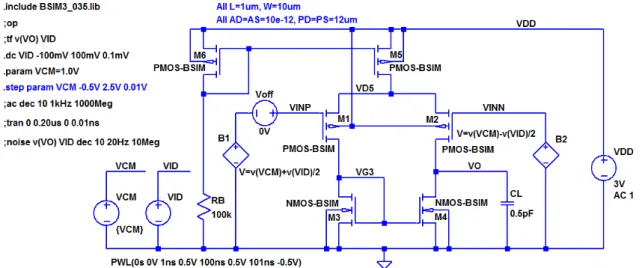
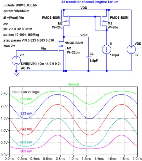
This is because in the gain expression, RIs now replaced by the small-signal output resistance of M2, and the total small-signal output resistance is the parallel combination of the output resistances of M1. For the schematic, you can also perform a DC sweep with the input voltage from −1.5 V to +1.5 V. With this value of the input bias voltage, the result of a '.tf' simulation is also shown in Fig.
An '.ac' simulation with Vid as the input signal results in a Bode plot for the output voltage as shown in Fig. The output voltage Hz can be plotted by showing the output node in the schematic. For the common-source amplifier shown above, design M1 so that the gain-bandwidth product of the phase is 50 MHz.
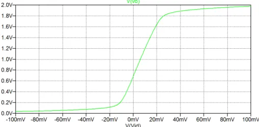
Find the DC bias value of the input voltage for which the output voltage is 1.5 V and find the gain of the small signal voltage at low frequencies. Find the open-circuit voltage gain and buffer output resistance for an input bias voltage of 0 V. For the telescoping cascode shown above, find the bias voltage value of VIN required to give an output voltage of 2 V.
For the folded cascode shown above, find the bias value of VIN required to provide an output voltage of 1 V.
Hierarchical Design
You may notice that the file name is the name of the circuit in Fig. By moving the terminals and drawing a triangular shape instead of the rectangular box, the symbol can be modified to look like in Fig. For the analytical approach, we base the design on the analysis of the two-stage opamp presented in Bruun (2019, Chapter 7).
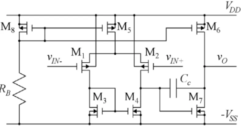
Both the closed loop performance and the loop gain should be simulated for a verification of the design requirements. Instead of specifying a resistor value RB, the bias current is set directly by a current source IB. From the error log file, you can also find the parasitic capacitances of the transistor calculated based on the dimensions of the transistor.
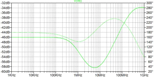
In the design, the relative increase of the bias current above the calculated minimum levels is greater for ID5 than for ID6. A re-simulation of the loop gain with Cc=0.80 pF results in the loop gain response shown in Fig. 5.19 and 5.20, we find that the design requirements of the opamp are met, so this completes the design of the opamp. The error log also reports empty pin currents for the input pins of the filter blocks.
When using filter blocks, you will undoubtedly encounter situations with multiple use of the same subcircuit. In this case, you should be able to specify different parameter values for different instances of the subcircuit. The filter blocks shown in Table 5.3 are also very suitable for investigating a feedback amplifier as designed in the example, we find that the transfer function of the amplifier at high frequencies is given by.
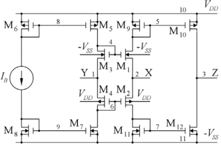
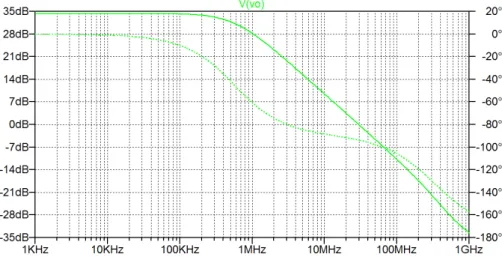
This means that VDD does not appear as a terminal in the symbols of the subcircuits, and at the top level of the circuit hierarchy, VDD must be declared as a global node using the SPICE directive '.global VDD'. This labeling of the wires going to the bus is what ensures the correct netlist for the diagram. Simulate the AC response of the closed-loop gain and the loop gain of the opamp shown in Fig.
Find the passband gain, the frequency at which the gain has its maximum magnitude and the magnitude of the peak in the frequency response. Find the propagation delay from the rising edge of the clock input to the Q output both for Q rising (tplh).
Process and Parameter Variations
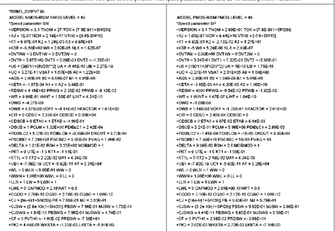
For the transistors, we need a speed parameter 'SN' for the NMOS transistor and another parameter 'SP' for the PMOS transistor. An examination of the BSIM3 models for the 0.35 µm process from (Chan Carusone, Johns & Martin 2014) shows that only five parameters differ for typical, fast and slow transistor models. For the output characteristics, the colors of the curves have been changed to match the colors used for fast, typical, and slow models for the input characteristics.
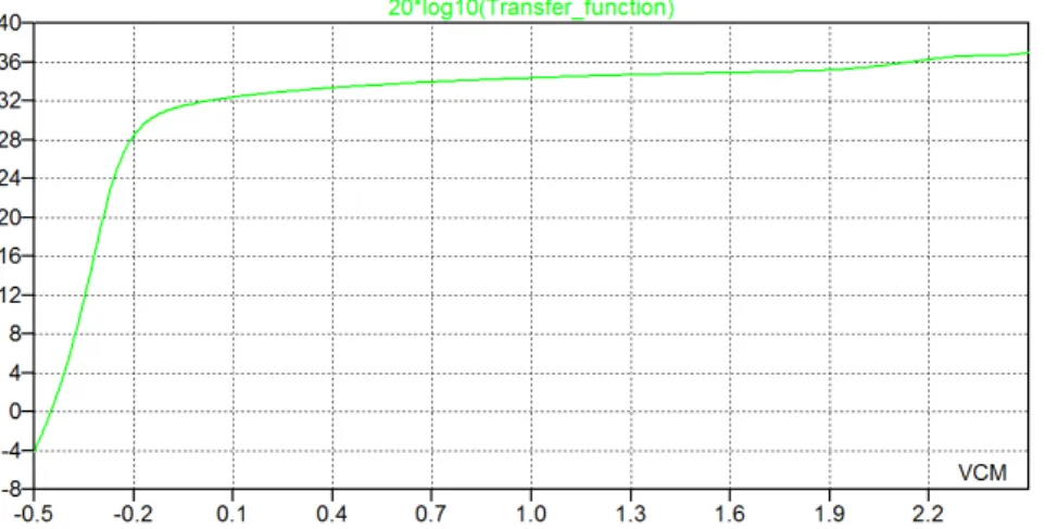
As a first investigation, we show the dc transfer characteristics of the process corners in Fig. The result of the '.ac' simulation is shown as a Bode plot of 'V(Vout)' in Fig. Often a more flexible way to establish the correct bias conditions for the '.ac' simulation is to provide a DC feedback from the output to the input.
6.15(a), this is achieved by inductive feedback directly to the gates of M1 and M2 and (high-bandwidth) AC coupling of the input voltage. For a temperature of 27 °C (green and blue trace), this graph can be compared with the GBW graph shown in the figure. When running a simulation with the speed parameters 'SN' and 'SP' varying through the process corners, you can search the process corners for propagation delays and rise and fall times.
When simulating PVT variations in the two-stage opamp of Example 5.2, it is necessary to define test benches that provide suitable bias conditions for the opamp regardless of the PVT variations. The optimization of the two-stage opamp for PVT variations is left as an exercise for the reader. For the purpose of this simulation, we assume that the threshold voltage has the nominal value of 0.57 V as shown in Fig.
For the common-source stage shown in Problem 6.3, find the worst-case unit-gain bandwidth corner (lowest unit-gain bandwidth) for temperature variations and supply voltage variations. Run a Monte Carlo simulation for the worst combination of temperature and supply voltage with stochastic variations of the process parameters of the transistors and capacitor CL. Estimate the mean and standard deviation of the unity gain frequency for the worst combination of temperature and supply voltage.
Importing and Exporting Files
In this editor, just change the file name in the line that specifies 'ModelFile'. In the specification of the supply voltages, you can use another parameter as shown in Fig. An alternative way to specify supply voltages and bias current at the top level of the circuit hierarchy is to introduce terminals for the supply voltages and bias current into the schematic symbol.
This is achieved by first specifying the terminals in the netlist description as shown in the figure. Consequently, below we change the default value of 'wdg' for the PMOS transistor to be the same as for the NMOS transistor. We can generate FinFET symbols from the netlist file in the same way as described in Example 7.2 for the current transporter.
In the auto-generated file, the full path to the model file '32nm_finfet.sp' is given. Using the 'Symbol Attribute Editor' ('Ctrl-A'), the parameter is inserted into the SpiceLine with a default value of F=1. In the same way, a subcircuit and a symbol for a single-gate PMOS FinFET (SGPMOS) can be designed.
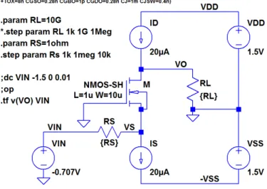
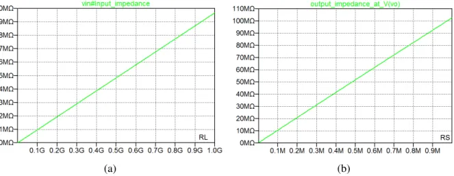
Each of the models is collapsed into a single, very long line in the expanded netlist file, so in Fig. Also find the small signal output resistance of the amplifier for the input bias resulting in the maximum absolute value of the gain. In the Mac version, the simulation results in a plot window where voltages and currents can be displayed.
Voltages and currents are selected by designating nodes or components in the schematic. Voltages and currents are selected by designating nodes or components in the schematic. In the Mac version, the simulation results in a plot window where the transfer function, input resistance and output resistance can be selected using the 'Add traces' command.
If you want to use only typical models, simply uncomment this command by deleting the "*" at the beginning of the command line. To include the speed parameters 'SN' and 'SP' in the model file, the parameters are process dependent.