A TECHNIQUE OF CONTROLLING AVALANCHE INJECTION IN A TRANSISTOR
BY
MD. AYNAL HAQUE
A THESIS SUBMITTED TO THE DEPARTMENT OF
ELECTRICAL AND ELECTRONIC ENGINEERING, BUET, IN PARI'IAL FULFILMENT OF THE REQUIREMENTS FOR THE DEGREE OF
MASTER OF SCIENCE IN ENGINEERING
DEPARTMENT OF ELECTRICAL AND ELECTRONIC ENGINEERING BANGLADESH. UNIVERSITY OF ENGINEERING AND TECHNOLOGY
MARCH, 1992 I
THESIS TITLE " A Technique of Controlling Avalanche Injection in a Transistor "
Name of the student Roll No
Regd. No
Md. Aynal Haque 891301P, Session 83207
1987-88
Accepted as satisfactory requirements for the degree (Electrical and Electronic).
BOARD OF EXAMINERS
in partial fulfilment of the of Master of Science in Engineering
1.
2.
~
(Dr. M. M. Shahidul Hassan) Associate Professor,
Department of Electrical and Electronic Engineering, BUET, Dhaka-1000, Bangladesh.
Sa.<fiJ
j£lt>.~~1...
(Dr. Saiful Islam) Professor and Head,
Department of Electrical and Electronic Engineering, BUET, Dhaka-1000, Bangladesh.
Chairman (Supervisor)
Member (Ex-officio)
3. ~ Tf,'f/"L-
(Dr. Md. Rezwan Khan) Associate Professor,
Department of Electrical and Electronic Engineering, BUET, Dhaka-1000, Bangladesh.
4~?~ (I);HOhllIIlIIIy)
Assistant Professor,
Department of Electrical and Electronic Engineering, BUET, Dhaka-1000, Bangladesh.
Member
Member
5.
Cif::;4 7/3191.-
(Dr. Md. Shamsuddin Ahmed) Professor and Head,
Department of Electrical and
Member (External)
This is to not been diploma.
CERTIFICATE
certify that this work has been done by me and it submitted elsewhere for the award of any degree
has or
Countersigned
.9$~
(Dr. M. M. Shahidul Hassan) Supervisor
Signature of the student
(Md. Aynal Haque)
CONTENTS
Acknowledgements Abstract
List of Figures
CHAPTER 1 INTRODUCTION
1.1 Historical background 1.2 Second breakdown
1.3 Thermal mode second breakdown 1.4 Current mode second breakdown
1.5 Current-voltage characteristics of transistors operating in CSB 1.6 Aim of the work
1.7 Summary of the dissertation
CHAPTER 2 OPTIMAL VALUES OF UNIFORMLY DOPED COLLECTOR PARAMETERS OF POWER TRANSISTORS
2.1 Introduction
2.2 Breakdown voltages of bipolar tmnsistors
2.2.1 Breakdown voltage of open-emitter transistor
2.2.2 Breakdown voltage of open-base transistor 2.3 Evaluation of optimal collector parameters 2.4 Conclusions
vi vii viii
1
3
4 6 8
13
14
16 16
17
18 22
32
CHAPTER 3 OPTIMAL VALUESOF COLLECTOR PARAMETERS OF HIGH VOLTAGETRANSISTORS WITH GRADED COLLECTOR
3.1 Introduction
3.2 Breakdown voltage of graded junctions
33 34
3.2.1 Single graded collector 34
54 61 62
3.2.2 Double graded collector 3.3 Conclusions
CHAPTER 4 CONCLUSIONS APPENDIX
A.Calculation of impurity gradient and depletion width for second portion of the 64 double graded collector
BIBLIOGRAPHY 67
ACKNOWLEDGEMENTS
The author would like to express his indebtedness and gratitude to his supervisor Dr. M. M. Shahidul Hassan, Associate Professor of Electrical and Electronic Engineer- ing Department, BUET, for his endless patience, friendly supervision and invaluable assistance in making a difficult task a pleasant one.
Thanks and indebtedness are to Dr. Mohammad Ali Choudhury and Dr. Moham-
mad Kaikobad for their helpful co=ents and suggestions.
0
The author wishes to express his thanks and regards to the Head of the Depart- ment of Electrical and Electronic Engineering, BUET, for his support during the work.
Sincerest thanks to friends and colleagues for their constant support and criticism of the reseBlchwork.
vi
ABSTRACT
Bipolar power transistors operated under reverse- biased condition are prone to failure due to the occurrence of current mode second breakdown (CSB). There are two parameters, critical current density and critical voltage, which measure the susceptibility of a transistor to this type of failure. Previous studies of CSB have demonstrated that the critical current density can be increased by increasing the collector doping density.
On the other hand, the collector density decreases with increase of breakdown voltage.
Therefore, this conflicts with the requirement to support a high breakdown voltage of a power transistor with uniformly doped collector.
A transistor with graded collector will offer more resistance to this failure. The transistor is usually designed to meet some requirements like specified breakdown volt- age, maximum current gain, etc. In this thesis, the optimal collector parameters of single and double graded collectors are theoretically evaluated under certain given con- straints. The results show that a double graded collector provides a substantial increase in doping density at the collector- substrate interface. For a specified breakdown volt- age, this increase in doping density at the interface provides a large increase in critical I:urrent density at the onset of avalanche injection. However, this results in high current protection with a small penalty in terms of collector width compareci. to that offered by
tm
optimized uniform colleCtor.vii
List of Figures
1.1 Temperature (T) and current density (J) distribution in (a) normal operation and 5 (b) electro-thermal runaway condition
1.2 Central injection from returning avalanche current of an n-p-n device 7 1.3 I-V characteristics obtained on small area mesa n+pn-n+ epitaxial transistors 9
pulsed into current mode second breakdown
1.4 Electric field distribution within the collector region 10 1.5 Schematic illustration of the movement of the field distribution with the rise of 12
collector current
2.1 Numerically computed collector doping density as a function of open-emitter bulk 19 breakdown voltage BVCBO
2.2 Numerically computed depletion width as a funciion of open-emitter bulk break- 20 down voltage BVCBO
2.3 Numerically computed peak electric field as a function of open-emitter bulk break- 21 down voltage BVCBO
2.4 Numerically computed collector doping density as a function of open-base bulk 23
breakdown voltage BVCEO
2.5 Numerically computed collector doping density as a function of maximum current 24 gain hFEO
2.6 Numerically computed peak electric field as a function of open-base bulk breakdown 25 voltage BVCEO
2.7 Numerically computed depletion width as a function of open-base bulk breakdown 26 voltage BVCEO
2.8 illustration of the relationship of depletion width W with collector doping density 27 Ne for a given breakdown voltage
2.9 Ionization rate as a function of electric field 29
viii
2.10 Numeric'l!!o' optimized collector doping 3S a function of open-base breakdown volt- 30 ageBVCEO
2.11 Numerically optimized depletion width as a function of open-base breakdown volt- 31 ageBVCEO
3.1 Proposed doping profile of a single graded collector 35
3.2 Flow chart of the computer program for optimization of collector parameters 37 3.3 Numerically computed peak electric field as a function of open-emitter bulk break- 38
down voltage BVCBO
3.4 Numerically computed initial doping density as a function of open-emitter bulk 40 breakdown voltage BVCBO
3.5 Numerically computed impurity gradient as a function of open-emitter bulk break- 41 down voltage BVCBO
3.6 Numerically computed depletion width as a function of open-emitter bulk break- 42 down voltage BVCBO
3.7 Numerically computed peak electric field as a function of open-base bulk breakdown
43
voltage BVCEO
3.8 Numerically computed initial doping density as a function of open-base bulk break- 44- down voltage BVCEO
3.9 Numerically computed impurity gradient as a function of open-base bulk breakdown
45
voltage BVCEO
3.10 Numerically computed depletion width as a function of open-base bulk breakdown 46 voltage BVCEO
3.11 Numerically computed doping density at the interface as a function of open-base 48 bulk breakdown voltage BVCEO
3.12 Numerically computed depletion width as a function of open-base bulk breakdown
49
voltage BVCEO
3.13 Numerically optimizJi peak electric field as a function of open-base breakdown 50 voltage BVCEO
ix
3.14 Numerically optimized initial doping density as a function of open-base breakdown 51 voltage BVCEO
3.15 Numerically optimized impurity gradient as a function of open-base breakdown 52 voltage BVCEO
3.16 Numerically optimized depletion width as a function of open-base breakdown volt-
53
age BVCEO
3.17 Proposed doping profile of a double graded collector 55
3.18 Numerically computed second impurity gradient as a function of open-base break- 57
down voltage BVCEO
3.19 Numerically computed width of the second portion of the collector as a function of 58
open-base breakdown voltage BVCEO
3.20 Numerically computed doping density at the interface as a function of open-base 59
breakdown voltage BVCEO
3.21 Numerically computed depletion width as a function of open-base breakdown volt- 60 age BVCEO
A.l Electric field distribution within the collector at a current density J(W1
+
W2)65
CHAPTER 1 INTRODUCTION
1.1 Historical background
The second breakdown phenomenon in transistors was first observed by Thornton and Simmons [1] in 1958, who described it as a new type offailure mechanism manifested by an abrupt reduction in the device voltage with a simultaneous internal constriction of current. Thornton and Simmons showed it to be a bulk, rather than a surface ef- fect. Over the years, several theories have been proposed to explain second breakdown
[2]-[7]: However, after further investigation, it was found that only three theories were acceptable. The first one is involved with a mechanism that is associated with forward biased second breakdown and was proposed by Scarlett and Shockley [5J. Under these conditions, device failure resulted from a lateral thermal instability that is followed by a thermal runaway condition. The other two theories attempt to explain reverse biased second breakdown and may be termed as the 'avalanche initiation' [6] and the 'thermal initiation' [1] processes. Avalanche process which causes current mode second break- down (CSB) is the cause and the thermal mechanis;n which may be termed as thermal mode second breakdown (TSB) will be the effect produced during sei~ond breakdown.
Sunshine and Lampert [7] investigated the hot filaments and established the processes responsible for failure. Their study consists of an analysis of the meciianism supported by accurate experimental data.
The theory for the explanation of current mode second breakdown was first pro- posed by Grutchfield and Moutoux [8] in 1966. The theory was extended by Hower and Reddi [6] in 1970 by taking into account of the final low voltage state. Leturcq [9] and also Hassan and Domingos [10] showed the susceptibility of failure of a bipolar transistor due to the occurrence orCSB during the switch-off period with an inductive load. The reverse-bias (turn-off) characteristics of high voltage fast switching n+pn- n+
1
power transistors have become important as these devices are used in increasing num- bers as high speed switches in power applications. Research to improve the device and circuit operating characteristics and to better model and understand their opera- tion is continuing. The phenomenon of CSB determines the reverse-bias limits of safe operation.
Re:ently, three researches on CSB have been completed [11],[12]'[13]. Rasul [11]
numeri£ally computed the critical voltage at the onset of second breakdown in bipolar power transistor switches driven with inductive load. He [11] studied the dependence of critical voltage on epitaxial layer thickness and collector doping density. Imtiaz [12]
studied the CSB phenomenon at the post avalanche injection condition. He [12] derived an analytical expression for sustaining voltage in terms of collector parameters when the traJlSistor is driven into CSB. Hasan [13] studied the effect of external inductance on inducing current mode second breakdown in epitaxial bipolar n+pn-n+ transistor driven with inductive load. He [13] analytically established an expression for critical inductance as a function of second breakdown current and collector parameters. He [13] also studied the pinch-in phenomenon in the base of a transistor at the onset of avalanche injection and found an analytical expression for critical current density at the onset ofavalanche injection. The critical current density fe.,t was found to be a function of dopillg density within the collector region. The above works [11]'[12]'[13] were carried out on8Il epitaxial bipolar n+pn-n+ transistor with uniformly doped collector.
From both theoretical and experimental viewpoints, efforts to solve the problems of second breakdown in transistors have only been partially successfull. Some progress has been made in the area of TSB. The identification of localized thermal runaway and the associated theory has led to the design of transistors [14] in which by using individual emittenesistors it is possible to limit the formation of regions of high current density and to substantially increase the range of power over which the device is thermally stable. But so far no significant success has been achieved in controlling current mode second breakdown. At large collector voltages, transistors are still susceptible to this undesirnble phenomenon, whose predominant feature is the transition to a low-voltage
2
high-current mode occurring at some critical points in the collector characteristic. To slow down the rise in device voltage during turn-off, an external protection circuit which is called a.'snubber circuit' is usually used [15]. However, the larger the transistor cur- rent, the larger the snubber power loss [16]. Recently, emitter-open base turn-off has provided superior transistor characteristics [17]. But the above mentioned techniques in- elude additional protection circuitry and are applied to a particular operating condition, namely, operation of power transistors with inductive loads where the main function of the circuits is to control the fast rise of voltage and current. On the other hand, Hassan and Domingos [18] showed that a substantial measure of protection against failure by avalanche injection can be built into the transistor by grading the impurity distribution of the collector.
1.2 Second Breakdown
The breakdown voltage of a power semiconductor device is one of its most important characteristics. Together with its maximum current handling capability, this parameter determines the power rating of the device. Second breakdown is one of the major causes by which the widespread operation of power transistors is liJIljted. It manifests itself internally by a sudden collapse of the collector-emitter voltage and the loss of control of the base drive due to simultaneous internal constriction of current. The decrease in voltage with the abrupt increase of current causes malfunction of the device and the extreme current concentration of the collector current over a very small area causes considerable heating which, in turn can result in device degradation or even catastrophic failure.
The phenomenon second breakdown is normally observed in power transistors, par- ticularly when driven with inductive load and it is manifested by either high power den- sity or high avalanche multiplication. Due to the wide scale use of power transistors, second breakdown has been the subject of extensive study. It is imperative to under- stand the second breakdown and to devise a protection scheme or an improved device
to avoid it. ,
t, Two mechanisms have been identified as being the causes of second breakdown,
i.e., heating and current injection. These two mechanisms are discussed in the following two sections.
1.3 Thermal mode second breakdown (TSB)
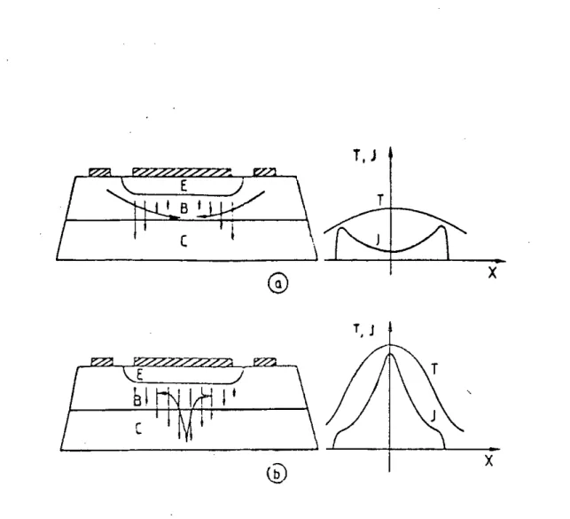
The thermal mode second breakdown (TSB) is induced by a local regenerative thermal runaway which develops as soon as a certain critical temperature has been reached within the active depletion region of the device. To understand TSB, consider a transistor the collector of which is maintained at a constant level by means of a control of the base drive. If, for any reason, a part of the active surface is heated, the collector current density will tend to increase in the region according to a positive temperature co-efficient. Consequently, there will be a decrease of current concentration in the rest of the device. Hence, any heterogeneity in the temperature distribution tends to concentrate the current lines in the hottest area, a phenomenon which leads to a further heating of that area. If the loop gain of the increased temperature and current densities at the hot spot exceeds unity, the transverse voltage drop due to the base current flow in the base region strongly influences the thermal runaway. The role of the base current is schematically illustrated in Fig. 1.1. In normal operation where power dissipation is at moderate level and temperature is not too high within the active region of the device, the current distribution would tend to concentrate towards the center of the structure as the result of spreading of heat flow within the crystal. This tendency is counteracted by the tendency for the current lines to crowd at the emitter periphery due to the effect of the centripetal base current flow ( Fig. 1.La). In this instance, distributed base resistance has a stabilizing influence. However, if for any reason the local temperature increases, the thermally generated current flowing through the collector bulk and space-charge regions progressively substitutes for the normal current. The external base current must decrease in order to hold the same level of collector current and the stabilizing influence of peripheral current is impaired. At high temperatures, the base current flow will be centrifugal in the hottest area thus enhancing the trend of the emitter and collector current distributions to concentrate towards the center of the structure ( Fig.
1.1.b) which develops instability.
T, J T
G)
XT, J
I
Jjc
W x
Fig. 1.1 Temperature (T) and current density (J)distribution in (a) normal operation and (b) electro-thermal runaway condition.
From the foregoing analysis, it can be concluded that TSB is initiated by current filamentation or the inhomogeneities in the device structure. It may occur below the breakdown voltage, but is generally observed when there is avalanche current present.
1.4 Current mode second breakdown
The most types of s~ond breakdown observed are probably caused by heating.
The second mechanism of failure of the device is electrically initiated and is called the current mode second breakdown (CSB). This second mechanism is due to avalanche injection caused by the electrostatic consequences of high mobile carrier density within the collector [9).
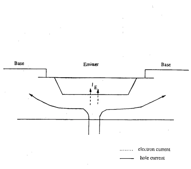
The mechanism tends to dominate at high collector voltages and under condi- tions that cause transient high current densities to occur locally within the device, for example, during the switch off period with an inductive load [19). CSB is, at least thea- retically, a non-thermal mechanism. The explanation involves the role of the free carrierr space-chargein the depletion layer of the collector-basejunction [10). At high current densities, these free charges can no longer be disregarded in relation to the charged impurities. When the collector current density exceeds the critical value Jo
=
qv.Nc ,wherev. is the saturated carrier velocity, q is the electronic charge and Nc is the col- lector doping density, the peak of the electric field no longer occurs at the metallurgical junction but at the interface between the lightly doped collector region and the highly doped substrate. This peak electric field increases with the collector current density and may reach values leading to avalanche multiplication. Current crowding occurs at the center of the emitter during this condition of operation. The crowding is caused by the center of the base- emitter junction being at a higher forward voltage than the edge, since the emitter to base contact resistance leads to a potential gradient in the base. This condition is shown in Fig. 1.2. The injected current gets multiplied in the collector, increases the base current and reinforces the central crowding. Hence, by regeneraiive action, the current increases rapidly and, at the same time is confined to a narrower area. The regenerative nature of this mechanism will ultimately allow high current densities to be reached within the central region. In a circuit incorporating a
Base Emiuer Base
=oJ \ , E. ,
I7 L
I I
cICClron currcnt hDle currclll
Fig. 1.2 Central injection from returning avalanche current for an n-p-n device.
collector load resistance this will cause a fall in collector voltage, a low voltage state associated with current mode second breakdown. The final voltage is much below the open-base breakdown voltage BVCEO'
Holesgenerated by impact ionization near the collector-substrate interface not only . produce a strong emitter-base forward biasing voltage but at the same time neutralize the charge of electrons and thereby decrease the electric field in regions outside the avalanche injection zone. As a result, the terminal voltage decreases with increase of current density. Fig 1.3 shows:the experimentally obtained I-V characteristics for . three mesa transistors of different sizes [20]. Practically, when conditions required for avalanche injection are produced, the electronic mechanism acts extremely rapidly. It accelerates the internal temperature rise and transfers to a thermally activated second breakdown condition.
1.5 Current-voltage characteristics of transistors operating in CSB
When current and voltage in a transistor exceed certain critical values, avalanche injection starts at the collector-substrate interface. The device then goes into CSB and shows negative resistance with further increase of current. At the onset of avalanche injection, the peak electric field shifts from the collector-basejunction to the collector substrate interface (Figs. 1.4 (a), (b) and (c) ). The current density at the onset of avalanche injection was given by [13]using the followingassumptions:
a. Recombination is negligible throughout the collector region.
b. Density of thermally generated carriers is small compared to the collector doping Nc.
c. Electron and hole saturated drift velocities are equal.
d. Only the drift component of currents needs to be considered.
Upon the above assumptions, the expression for critical current density is given by [13]'
EV.
Jr:ril
=
Jo+
TEc (1.1)where L is the width of the collector layer and Ec is the peak electric field at the collector-substrate interface at the onset of CSB.
50
epitaxial transistors
)0
~Wepi
-+-
'rm'
10 2
1
o o
20VCE (voila)
Fig. 1.3 I-V characteristics obt~ed on small area mesa n+pn-n+
pulsed into current mode second breakdown.
Ie lamps)
3
, "'."
9
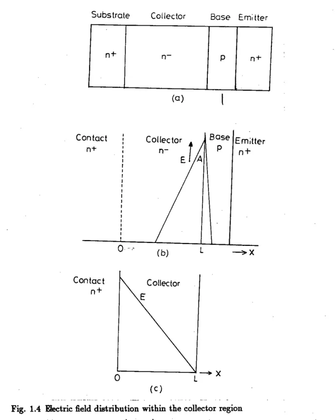
Substrate Collector Base Emitter
n+
(a)
p n+
Contact n+
( b) L
Base Emitter
P
n+
Contact n+
o
Collector
(c)
---+X L
Fig. 1.4 Electric field distribution within the collector region (a) Structure of an n+pn-n+ bipolar transistor
(b) Field distribution within the collector-base junction at low current (c) Field distribution within the collector region at J
>
Jo.The ionization rate of carriers is a strong function of electric field and at the onset of avalanche injection generated carrier is small. Therefore, variation of the electric field due to the collector doping density and epitaxial layer thickness is not significant.
The critical current density 1. that initiates CSB is necessarily limited by the collector doping density capable of supporting the open-base breakdown voltage BVCEO' But for a specifiedcurrent gain hFEO and breakdown voltage BVCEO , the collector doping density becomes constant. Therefore, using a transistor with uniformly doped collector, an increase of critical current density can not be achieved [18).
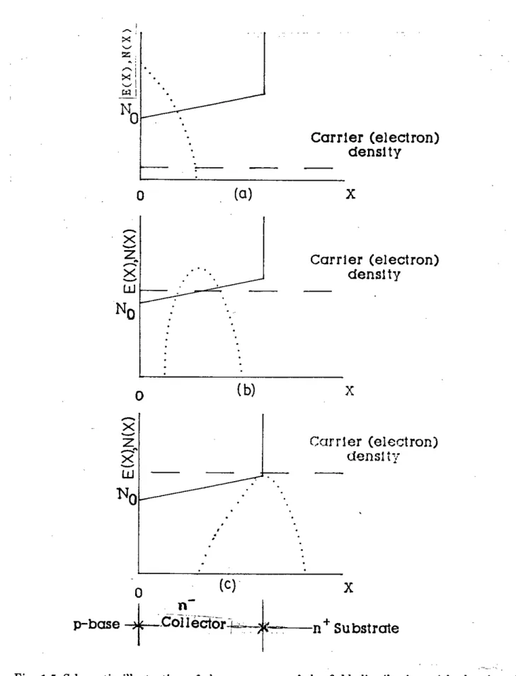
Introduction of a graded doping concentration throughout the epitaxial collector layer introduces an additional design parameter that allows control over both the re- quired voltage and the critical current density for the onset of avalanche injection. Fig.
1.5 shows conceptually the potential advantage expected to be gained from a linearly graded collector layer. At low currents, the value ofBVCEO is determined by the col- lector impurity profile and the current gain of the transistor. When 1
<
10,where, 10=
qv,No, the peak of the electric field will occur at the collector-base metallurgi- cal junction and the electric field will follow the distribution 88 shown in Fig. 1.5 (a).Ii the current density exceeds 10,the peak of the electric field will move towards the collector-substrate interface and the field distribution in that case is shown in Fig. 1.5 (b). Ii the peak of the electric field occurs at a distance z, the corresponding current .'density must be equal to the value ofqv.(No
+
az). Poisson's equation for the gradedprofile'~anbe written 88,
~: =
~(n - N(z)) (1.2)where, N(z) =No
+
az. In eqn. (1.2), holes are neglected. Introducing 1=qv,n and Jo(z)=
qv,N(z), eqn. (1.2) can be written in the following88,dE 1
dz
=
€tI, (J - 10(z)) (1.3)When 1
=
Jo(z), the field gradient at z is zero i.e, ~=
0.' The above analysis shows that for a graded collector profile, the peak electric field moves towards the collector-:
o
o
(0)
(b)
•
.
CarrIer (electron) densIty
x
CarrIer (electron) densIty
x
Cmrler (electron) densltv•
x
o (C)
p-b",. +.coi~C!or~t'-. -.
--n + SubstrateFig. 1.5 Schematic illustration of the movement of the field distribution with the rise of conector current. - for N(X) and ... for E(X).
substrate interface with an increase of collector current density. On the other hand, when J = Jo(W)
=:
qv,(No+
aW), the peak electric field will occur at the collector- substrate interface. With further increase of current density the peak will still occur at the interface and its magnitude will increase to sustain a constant breakdown voltage.The substrate is heavily doped and the electric field will decrease sharply unless the current density J exceeds Jo, where, Jo
=
qv,NDs. Here, NDS is the doping density of the substrate. For large NDS, Jo will be very high and at finite current density J, the field distribution will not change its size. As the current density increases, the peak electric field progressively transfers across the epitaxial layer in a controlled manner, and the maximum sustainable voltage will not fall below the low current value until the condition depicted in Fig. 1.5 (c) is exceeded. For this to occur, the current density must reach a value [18]'Jc
=
qv,(No+
aW) (1.4)where,
No=collector doping at the collector-base interface a
=
collector impurity gradientW
=
epitaxial layer thicknesswhich can be arranged to be significantly higher than would be possible with a uniformly doped collector layer capable of supporting the same voltage.
1.6 Aim of the work
Continuous improvements in the field of technology, transistc)r physics and design procedures have made it possible to use bipolar transistors in the area of power ap- plications upto 100 kVA. The control of deep diffusions and thick epitaxies with low impurity concentrations has led to great improvements in structure designs. Thus, bipolar tnmsistors have now come of age and are already the preferred devices for a variety of applications such as choppers, inverters, microwave devices, submarine cable transistoIll, etc. On the other hand, second breakdown imposes a limit on the current handling capabilities of bipolar power transistors, specially when their voltage blocking
capability is high. A transistor used as a switch is more prone to failure due to the occurrence of CSB. A success has been achieved in avoiding thermal mode second breakdown. But, so far a partial success has been achieved in avoiding CSB.
'The main objective of this work is 'to show that the avalanche injection can be controUed significantly by using graded collector doping.
1.'T Summary of the Dissertation
A recent work f18) on graded collector has demonstrated the beneficial effect of graded collector in terms of resistance to CSB over that of uniformly doped collector.
But the analysis was carried out for only single graded collector with the current- voltage characteristics of single graded collector. The analysis was carried out under the followingassumptions,
a. Peak electric field at breakdown Ee is insensitive to the epitaxial layer thickness.
b. The functional dependence of Ee upon open-base breakdown voltage and current gainhFEO derived for uniformly doped collector is also used for graded collector.
c. Cakulation of No , a and W are made considering the same resistance used for uniformly doped collector for a specified breakdown voltage and current gain hF EO,
The peak electric field at breakdown has dependency not only on doping density and current gain hF EO but also on epitaxial layer thickness. The peak electric field Ee follows.a different functional dependency on breakdown voltage and current gain.
In this thesis, peak electric field under breakdown condition is numerically calculated and an empirical relationship is derived from numerically obtained data. In designing optimal parameters of the single graded collector of a transistor, the collector region is optimized to minimize the collector resistance. Analysis shows that no significant increase in doping density at the collector-substrate interface can be obtained with a single graded collector. However, transistors with double graded collector offer the prospect of achieving a substantial measure of protection against failure from CSB under any operating condition.
The optimal parameters of uniformly doped collector have been evaluated in chapter 2 and those of graded collector in chapter 3. In chapter 3, the optimal parameters of graded collector have been compared with those of uniformly doped collector to show the relatively high second breakdown ruggedness of graded transistors. Both single graded and double graded impurity profiles have been considered. The empirical expressions of the collector parameters as a function of breakdown voltage are derived in chapters 2 and 3. Calculations are carried out for optimal collector parameters to achieve minimum resistaJK:e for a specified breakdown voltage. The analysis shows that a substantial increase in doping density at the collector-substrate interface can be achieved with a double graded collector and thereby, the device is less prone to failure due to avalanche injection.
,
CHAPTER 2
OPTIMAL VALUES OF UNIFORMLY DOPED
COLLECTOR PARAMETERS OF POWER TRANSISTORS
2.1 Introduction
Design of a power transistor always involves optimal calculations of collector doping and collector width for a desired value of blocking voltage specified either in terms of open-base breakdown voltage or open-emitter breakdown voltage. Also to reduce the power dissipation within the collector, the transistor is designed to keep the resistance of the collector a minimum. In designing a transistor, closed form expressions for collector doping density and collector width are often used. In this chapter, the relationship between the optimal parameters of collector with the breakdown voltages is established.
2.2 Breakdown voltages of bipolar Transistors
Avalanche breakdown voltage imposes an upper limit on the reverse bias for most diodes and on the collector voltage of bipolar transistors. However, in the usual common- emitter configuration, current amplification interferes with avalanche multiplication and imposes other limitations. The doping density of the base region of an epitax- ial n+pn-n+ bipolar power transistor is much higher than that of the collector region and therefore, the base-collector junction can be considered as a one-sided p+n junction for determination of the bulk breakdown voltage of the junction.
For a uniform collector doping density of Nc, the electric field within the depletion region of the collector side of collector-base junction is given as [21],
E(z) = Ec _IJ..Ncz (2.1)
E
where Ec is the peak electric field at the collector-base junction. At the boundary, E(W) = O. Using this boundary condition, eqn. (2.1) can be written in the following form,
Ee = -NeWq
f (2.2)
The voltage under this field distribution is,
(2.3)
(2.4) The above two equations can be used in determination of breakdown voltage of the junction.
2.2.1 Breakdown Voltage of Open-emitter transistor
For an open-emitter transistor, threshold condition for avalanche breakdown in a one-sidedp+n junction where the avalanche multiplication is initiated by holes can be expressed as [22],
la
w -1.'
(a.-an)d ••,
J_ - 1OIpe 0 •••• -
o
where/lp and OIn represents the ionization rates of holes and electrons respectively and W is the thickness of the epitaxial layer at breakdown. The field dependence of the ionization rates 01can be expressed as,
(2.5) The values of A and b for electrons and holes are given by Van Overstraeten and de Man [22].-For transistors with open-emitter, open-emitter bulk breakdown voltage BVCBO is equal to the breakdown voltage of an isolated p+n (collector-base) junction.
The bulk breakdown voltage BVCBO is, therefore, given by equation (2.3) and is written as.
(2.6) In carrying out the integration of eqn. (2.4), a powerful and efficient numerical -technique, Romberg integration is used. For a given BVCBO' a choice of E
e
will giveNe and W using eqns. (2.2) and (2.6). For a particular value ofEe ,ionization integral will be equal to unity. From this computed value ofEe , Ne and W can be obtained.
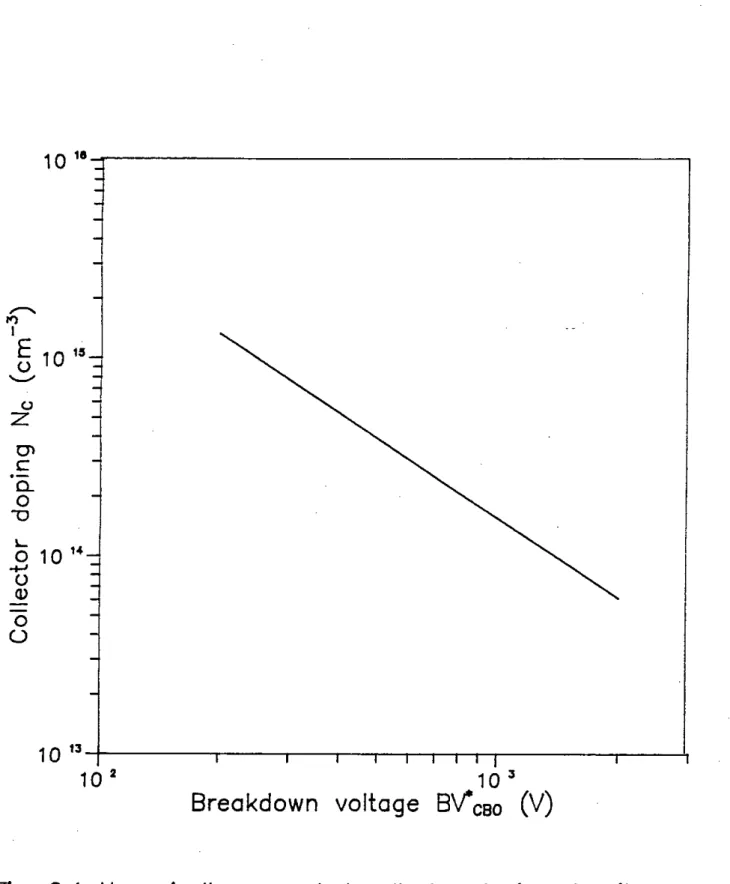
Figure 2.1 shows the numerically computed doping density Ne as a function of bulk breakdown voltage BVCBO of an n+pn-n+ transistor with uniformly doped collector.
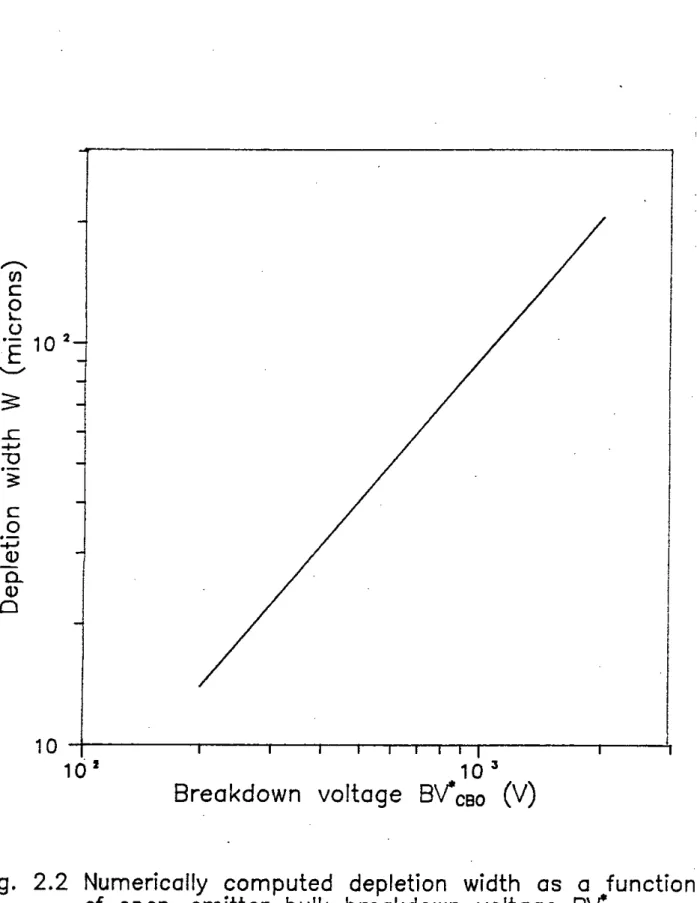
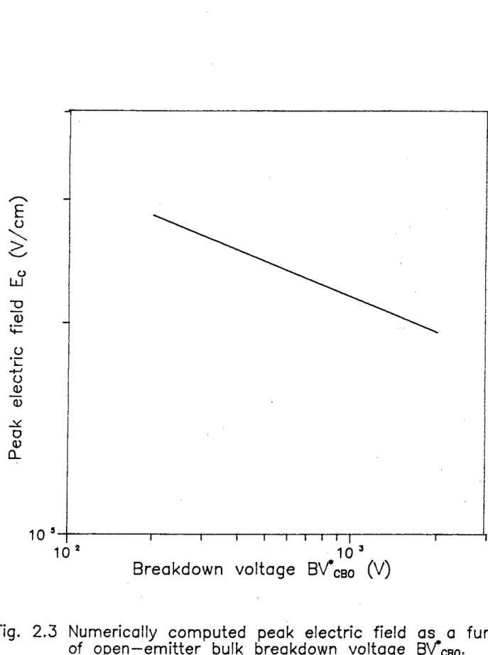
Figure 2.2 shows the computed depletion width W while Figure 2.3 shows peak electric field Ee as a function of bulk breakdown voltage BVCBO'
The empirical expressions for Ne, Ee and W are given by,
Ee
=
6.89 x 10sB".YeBo'_.lW
=
2.9 X 10⁻⁶ BVCBO i
em-3
Vlem
em
The collector doping density decreases with incre8.l!le in breakdown voltage while the depletion width increases with increase in breakdown voltage. For transistor with higher breakdown voltage, the collector doping density will be of the order of 1013 to 1014cm-3•
2.2.2 Breakdown voltage of open-base transistor
For ajunction transistor, the maximum collector to emitter breakdown occurs at the voltage BVCEO; where the product of the low voltage current gain a and the collector ava.la.nche multiplication M is unity. For silicon transistor, the thermally generated currents within the collector-base junction is much greater than the minority carrier diffusion current entering the reverse-bias collector junction from the collector region.
In ca.lcula.tion of open-base breakdown voltage, thermal generation within the collector junction needs to be considered .. The condition for avalanche breakdown in the case of
open-base transistor can be expressed as [23J,
(2.7)
10 I'
,..."
I')
I
E
10 IS()
'--"
<.J
Z
01
.-
C0..-0
o
l....
o
10 14 -+J() (l)
U
o
10 13
10 2 103
Breakdown voltage BV'cBO (V)
Fig. 2.1 Numerically computed collector doping density as a function of open-emitter bulk breakdown voltage
aV*CBO'19
•••...
(JJ
c
0I- ()
il
.- 10 2
'-'" E
3
..c
+' '"0.-
3:0
c
:;:;
(1)
0.
(1)
0
103
Breakdown voltage Bv*cBO (V)
Fig. 2.2 Numerically computed depletion width as a function of open-emitter bulk breakdown voltage
Sv*C80.20
•
10
JBreakdown voltage BV'cBo (V)
•...•..
E
u;; '-./
()
W -0
.-
'+-Q)'i:u
-+-'u
Q)
Q)
•
"',
~ 0
Q)
ll..
Fig. 2.3 Numerically computed peak electric field as a function
of open-emitter bulk breakdown voltage BV'CBO'
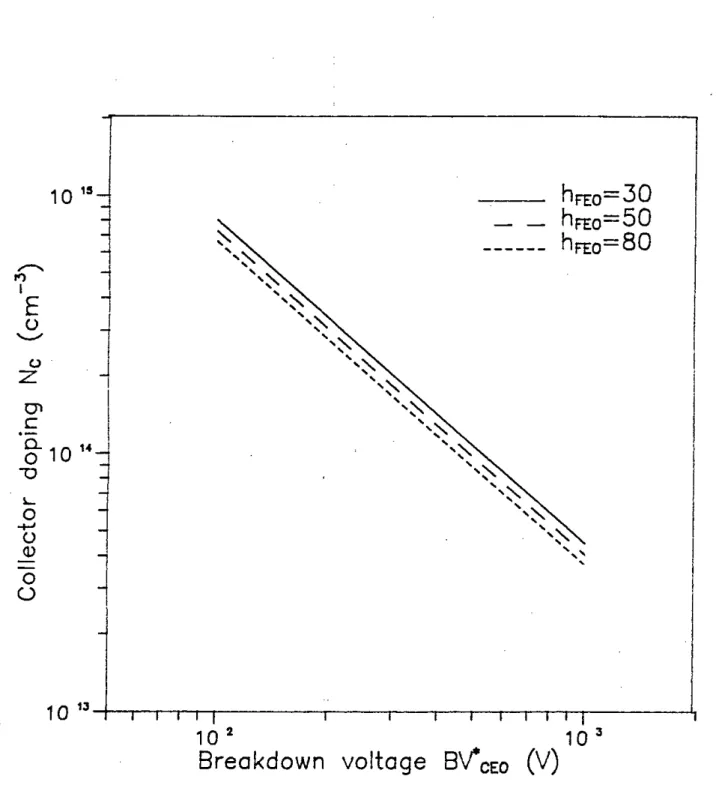
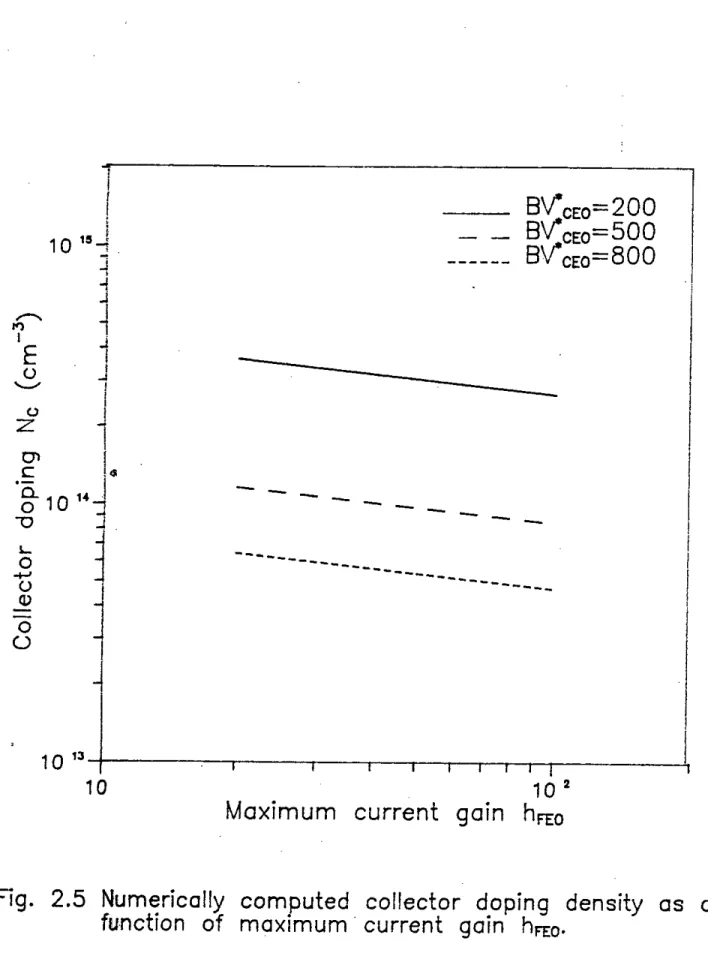
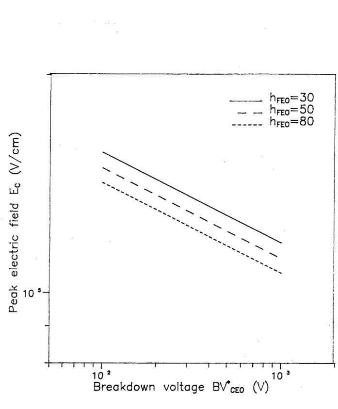
Figure 2.4 shows numerically calculated collector doping density Nc as a function of open-base bulk breakdown voltage BVCEO for three different values of hFEO• For a given"FEO, Nc decreases with an increase in BVCEO' Fig. 2.5 shows Nc as a function ofhFBO for three different values ofBVCEO' For a given breakdown voltage, the doping density increases with a decrease of hFEO. The variations of peak electric field Ec and depletion width Was a function ofBVCEO for different values of hFEO are plotted in Figs. 2.6 and 2.7 respectively.
The empirical expressions for Nc, Ec and Ware given as,
2.3 EwJ.uatioD of optimal collector parameters
With regard to collector width W, the obvious choice would be to allow the depl&- tion IllJer to spread freely under sustaining breakdown voltage. However, a moderate reduction ofW'within the value ofWc to a free extent of the depletion layer width can' lead to an advantageous rise in maximum collector current. In order to avoid affecting the voltage blocking ca~ability, such a reduction must be accompanied by a decrease in collector impurity concentration Nc [9]. This is qualitatively explained in Figure 2.8.
In previous works, the optimal values of Nc and W for a specified breakdown voltage have been obtained under the assumption that the peak electric field for the reach-through case will not differ from the bulk case. This results an underestimate of the peak electric field, and therefore, an underestimate of open-base breakdown voltage BVCEO' In the evaluation of optimal values of Nc and W for a given breakdown, the peak electric field at breakdown under fre&-extent and reach-through depletion layer condition has been considered to be the same i.e.,insensitive to the epitaxial layer thick-
IIi
.--...
I"l
I
E
()
'-"
u Z
10 15
"1
j
h FEo =30 h FEo =50 h FEo =80
,
:'j
10 13
102 103
Breakdown voltage B'!'cEO (V)
Fig. 2.4 Numerically computed collector doping density as a
function of open-base bulk breakdown voltage B'!'CEO.
---
--- ---
------- ---
iii I
10
2Maximum current gain h
FEO- -
- - ---- - -
Fig. 2.5 Numerically computed collector doping density as a
function of maximum current gain h
FEO•1
() -+oJ
'c
() (l) (l)
2 10'l
0-
I
l
i10
I 2Breakdown
I II I
10 3
voltage Bv"CEO(V)
Fig. 2.6 Numerically computed peak electric field as a function
of open-base bulk breakdown voltage Bv"CEO'
c o
.-
-+"Q)
0-
o
Q). - -
i
I .---
...---.
\~ 10
2~! ~ 1
j
j
10
I I 10 2
Breakdown
i I I I 10 3
voltage BV'
CEO(V)
Fig. 2.7 Numerically computed depletion width as a function of open-base bulk breakdown voltage 8v"CEO'
26
---,
I
I
... :
Increasing NC
w
"0
C11 -...
..•... ..~•. ~
w
Fig. 2.8 lliustration of the relationship of depletion width W with collector doping density Ncfor a given breakdown voltage.
27
ness. However, in this thesis, fixed electric field for BVCEO is not used in the evaluation of optimal parameters of the collector.
The electric field at the collector-substrate interfa.ce ~ be given by, E1 =Ee - -NeWq
!
The voltage supported under this field distribution is,
BVeEo
=
EeW - '!'NeW22!
Also the collector resistance per unit area is given by,
(2.8)
(2.9)
W
R= qJ!nNe (2.10)
where Pn is the electron mobility within collector region.
Optimal values ofNe and W can be obtained by simultaneous solution of equations ( 2.8). (2.9) and (2.10) together with the ionization integral ( eqn. 2.7) for a specified breakdown voltage.
Ionization rate is a strong function of electric field and the ionization rate is negli- gible far the field below 8 x 10⁴ V/cm (Fig. 2.9). To minimize error in the calculation of ioniza.iionintegral, the electric field E1 at the collector-substrate interface is not a.llowed to take a value above 8 x 10⁴ V/ em.
The optimized collector doping density Ne and depletion width Ware respectively plotted in Figs. 2.10 and 2.11 as a function of three values,~r hFEO' The empirical expressions for optimized values of Ne, Ee, Wand R can be written as,
-I-'(l)
o
l..-:;
-!
10-3
1
:::
-
10
-4.j
"' :I L..J ••••
-
~10 -5-4
~.
1 0 -8~
10 ...•
" "-
"- , , , ,,
\
\
\
\
\
\ 0<
\ p
\
\
\
\
\
\
\
\
\
\
\
\
\
I I I I I
10 -5
Inverse of electric field
I
l
1 IE (cm/y)
Fig. 2.9 Ionization rate as a function of electric field.
29
10"~
I'l
r--.
I
! 1
z
()L
o
-+-'()
Q.J
U
o
h
FEo=30 h
FEo=50 h
FEo=80
10
3Breakdown voltage BV cEo
(V)Fig. 2.10 Numerically optimized collector doping density as a
function of open-base breakdown voltage BV
CEO'1
I
j-'--I
,. -
I ,---
,.-....
,~ 10'j
.- I
E i
;; j
~ 1 o l
-+-'Q)
0-Q)
o
I
10 ~~----~--~-~-~~~i -1r---Ti~1---J,
102 10
3Breakdown voltage BV cEo
(V).Fig. 2.11 Numerically optimized depletion width as a function
of open-base breakdown voltage 8V
CEO•2.4 Conclusions
Epitaxially grown base-collectorjunctions with a lightly doped collector are widely used in the fabrication of power transistors. Breakdown voltages of epitaxial bipolar n+pn-n+ transistors are numerically computed based on the more accurate ionization rates of R. Van Overstraeten and H. de Man [22]. The optimal values of collector dopingdensity Ne and the epitaxial layer thickness W subject to a minimum collector resisianceare numerically computed. Empirical expressions for optimal parameters Ne and W are also established.
In the evaluation of optimal parameters, the peak electric field for bulk breakdown is not used. By using the empirical expressions for Ne and W, more accurate values of other parameters of a transistor can be obtained.
32
!..};.
CHAPTER 3
OPTIMAL VALUES OF COLLECTOR PARAMETERS OF mGH VOLTAGE TRANSISTORS WITH GRADED COLLECTOR
3.1 Introduction
Works on current mode second breakdown show that a substantial measure of protection against failure by avalanche injection can be built into a transistor by grading the impurity distribution of the collector [18). The improvement is achieved directly from a substantial increase in the collector current required to trigger avalanche injection.
The current that initiates avalanche injection depends upon the doping density at the collector-substrate interface and it increases with the increase of doping density at the interface. The collector doping is optimized to achieve the minimum collector width for a specmed blocking voltage.
A graded collector impurity profile allows the current density to increase while pre- venting the maximum electric field from reaching a value that permits carrier multipli- cation. Appropriate collector design can make the critical current density considerably higher than would be possible with a uniformly doped collector designed to support the same breakdown voltage.
For single graded collector, the initial doping density and impurity gradient can be obtained for breakdown voltages specmed either in open-base or in open-emitter condi- tion 'under the requirement of achieving minimum collector resistance at free spreading of the depletion layer into the collector region. But a signmcant increase in current den- sity requires a very thick collector layer, particularly in the case of high voltage power transistor. This has a detrimental effect on the performance of the transistor and for the base drive required to hard saturation, and introduces technical problems concern- ing epitaxial layer growth. These difficulties can be eased considerably by using double graded collectors. This chapter deals with the determination of optimal parameters of
single and double graded collector of high voltage transistors. The optimal values of graded collector parameters will be compared with those of a uniformly doped collector.
3.2 Breakdown voltage of graded junctions
The doping density of the base region of an epitaxial bipolar transistor is much '1 higher than that of the collector region and therefore, the base- collector junction can be considered as a one-sided p+n junction for determination of the bulk brea.kdown voltage of the junction. For a one-sided graded junction, the brea.kdown voltage can be determined by the collector doping at the collector-base interface and the collector impurity gradient. For the open-emitter transistor, the avalanche brea.kdowncondition can be expressed by eqn. (2.4). For convenience, the eqn. (2.4) is again written below,
l
w -1."
(a.-a. lei.,Id - 1Ctpe 0 z -
o
&r an open-base transistor, the brea.kdown condition is given by,
(3.1)
(3.2)
Eqns. (3.1) and (3.2) are used for determination of brea.kdown voltages BVCBO
and BVCEO respectively. However, to solve the ionization integral, the mathematical expressionfor field distribution within depletion region is required.
3.2.1 Single graded collector
The doping profile of a single 'graded collector is shown in Fig. 3.1. The impurity concentration in the collector region is,
Nc(z)
=
No+
aW(z)where,
No= collector doping at the base-collector interface a= collector impurity gradient
W
=
collector layer width34
(3.3)
:>,
.,jJ.-{
~ impurity
gradient
c
OJa.
"0 CJl
.
C.-{0..
NO
.g
x
I~.•. ~---w--- ..• 1 Collector
Base~ll~c~ C_o_l_l_e_c_t_o-r-e_p-i_~_a_X_l_'a-l-l_a_y_e_r __ -...Isubstrate
Fig. 3.1 Proposed doping profile of a single graded collector.
Solution of one-dimensional Poisson's equation leads to the expression for electric field within the collector as,
q( 1 2)
E
=
Ec - - Noz+
-azf 2 (3.4)
Integrating eqn. (3.4) and using boundary condition, E
=
0 at z=
W, it can beshown that,
VB
=
EcW _ qNow2 _
qaw3
2f 6f
Also, the depletion layer width at breakdown is,
(3.5)
W=--+
Noa
(N
-
o)2+-
2f Eca qa (3.6)
for wider epitaxial layers that are able to contain the full depletion width.
The collector resistaxice per unit area is,
(3.7) Unfortunately, eqns. ( 3.3), (3.4) and ( 3.7) do not lead themselves to convenient analytical expressions for the values of No, a and W corresponding to minimum resis-:.
tance. Instead; .the solution has been obtained using the computer iteration procedure •.
shown .in figure 3.2. Romberg integration is used to carry out the integration of eqns.
(3.1) and (3.2). Solving eqns. (3.5) and (3.6) together with satisfying ionization integral i.e., eqn. (3.1) or (3.2) as specified by the breakdown, a number of collector parameters are found. The combination of parameters which minimizes the collector resistance is the optimum combination.
The peak field at breakdown Ec, obtained from the iteration procedure is shown in Figure 3.3 as a function of open-emitter bulk breakdown voltage BVCBO' Ec decreases with an increase in BVCBO -due to the widening of the depletion layer.
No
No
start
rake specified
•••alue of BVc~o
InitializE' N",
Initialize Ec
Sol •••e eqns.3.5 &
3.6 siMultanE'ous- ly to get If & a
Sol •••e E'qn. 3.1
Sol •••e eqn. 3.7 for R
Fig. 3.2 Flow chart of the computer program for optimization of collector parameters.
l I
tI
,... 1
IE
Ii
u
;; I I
'--'
I0 I
W
-0
I
(l) I
;,;:: II
II
U I
.>:
I+J
u I
(l) ,
(l)
I
I
..:£.
0 t
(l) I
0... I
I
I103