The layout design of the 5-input reconfigurable ranking filter is also done in this work. Layout design of the ranking filter for window size N = 5 Simulation result of ROF from extracted netlist for N = 5 and 1'=3.
LIST OF TABLES
INTRODUCTION
- Introduction
- Literature Review
- Objective of this Thesis Work
- Thesis Outline
Mixed signal order filters [19] are more susceptible to noise compared to fully digital filters. Make it possible to reconfigure the order filter so that any element of the order can be retrieved as the filter output.
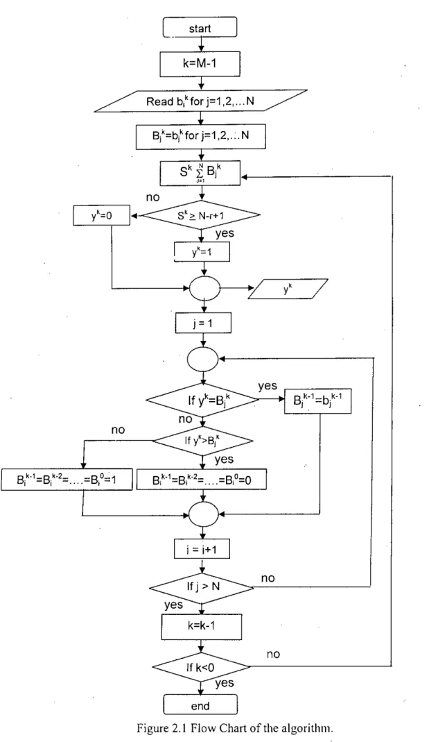
ALGORITHM OF THE RANK ORDER FILTER
- Introduction
- Algorithm Description
- System Level Implementation of the Algorithm Using Simulink
- Simulation Results
- Conclusion
During each iteration of the algorithm, k-th bits of all five elements are added for calculation. In the example given in Figure 2.5, the maximum sample should be the result according to the algorithm, since the value of 'r' is '5'.
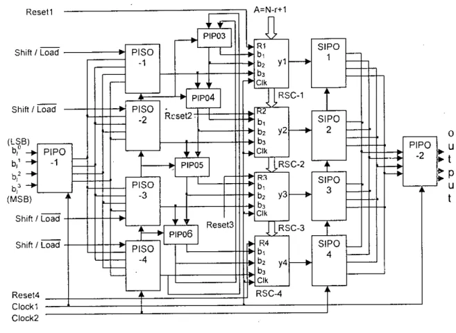
ARCHITECTURE OF THE RANK ORDER FILTER
- Introduction
- Architecture Description
- Bit Update Circuit (BUC)
- Parallel Counter Circuit
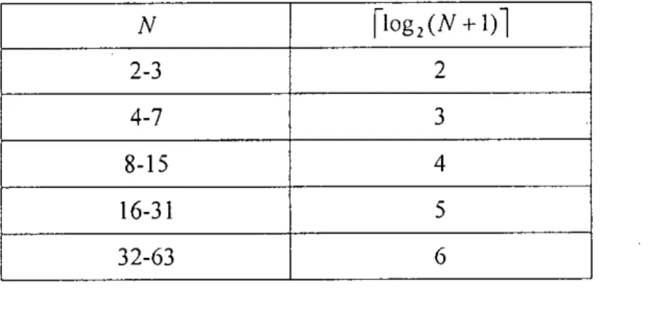
- Comparator Circuit
- Operation of the Rank Order Filter
- Introduction
- Maximum Filter
- Minimum Filter
- Median Filter
- Five-input Median Filter
- Seven-input Median Filter
- Nine-input Median Filter
- Fifteen-input Median Filter
- Conclusion
The output of the comparator circuit is the desired output from the sequence select circuit (RSC). In Figure 4.5, E/ represents the MSB of the output of the Parallel Counter circuit and El represents the LSB. To design a 7-input averaging filter, the reconfigurable first-order filter comparator circuit can be eliminated.
In all these cases, the MSB of the output of the Parallel Counter circuit is '1'. Therefore, the MSB of the output of the Parallel Counter circuit can be treated as the output of the Median filter. So two Full Collectors of the Parallel Counter circuit can be replaced by two Cry Out Generator circuits.
The output of the VHDL model of the 7-input media filter with the Spartan2E-xc2S50e target device is shown in Figure 4.8. To design an I S input averaging filter, the Comparator circuit of the reconfigurable rank order filter can be eliminated. In all these cases, the MSB of the output of the Parallel Counter circuit is 'I.
So three Full Adder of the Parallel Counter circuit can be replaced by three Carry Out Generator circuits.
RANK ORDER FILTER WITH INCREASED THROUGHPUT
- Introduction
- Modified ROF Architecture
- Overview and Comparison
- Conclusion
The output of the 2nd data window is obtained from the 4th clock pulse at the RSCA output. The output of the 3rd data window is obtained from the 5th clock pulse at the output of RSC-1. The output of the 4th data window is obtained from the 6th clock pulse at the output of RSC-2.
The output of the 1st data window is obtained from the 5-hour pulse at the output of the RSC-5. The output of the 2nd data window is obtained from the 6th clock pulse at the output of the RSC-6. The output of the 3rd data window is obtained from the 7-hour clock pulse at the output of the RSC-l.
The 4[h data window output is obtained from the 8[h clock pulse at the output of RSC-2. The output of the 5[hdata window is obtained from the 9[hclock pulse at the output of RSC-3.
LAYOUT DESIGN AND TRANSISTOR LEVEL SIMULATION OF THE RANK ORDER FILTER
Introduction
The Bit Update Circuit
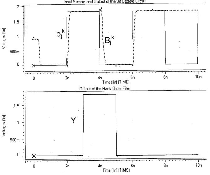
For a given input sample h/ and for a test output of the ranking filter Y, the HSPICE simulation output B/ of the EVC is shown in Figure 6.2 with a dotted line. The simulation of the EVC circuit assumes a delay of Ins, which is the maximum allowable delay at the output of the ROF for a clock speed of 500MI-Iz. From Figure 6.2 it can be seen that the EVC works well and as the number of inputs to the Rank Order Filter increases, the delay in the EVC has no effect on the output of the ROF because all EVCs in an ROF work in parallel. ,.
Figure 6.2 shows that the rise time and fall time of the ROF are not the same because the width of all the transistors used to implement the EVC was assumed to be the same. After changing the W/L ratio of the NMOS transistors, the fall time of the modified SUC is reduced by almost 20 ps. Another important change is that initially the SUC output should be '0' volts relative to the inputs.
While in figure 6.2, it is found to be 0.9 volts due to high resistance of NMOS transistors. However, when the resistance of the NMOS transistors decreases by increasing the W/L ratio, it turns out that the output of the SUC is
The Parallel Counter Circuit
To decrease the fall time, the channel width of some of the NMOS transistors of the NAND gates used to implement the closed D-latch of the SUC is increased so that they discharge quickly. After increasing the channel width of the NMOS transistors of the NAND gates of the BUC by 0.36 1lI11, the W/L ratio of the NMOS is doubled and the obtained output of the modified BUC is shown in Figure 6.3. As the number of input samples in the memory window to be sorted increases, so does the number of binning stages.
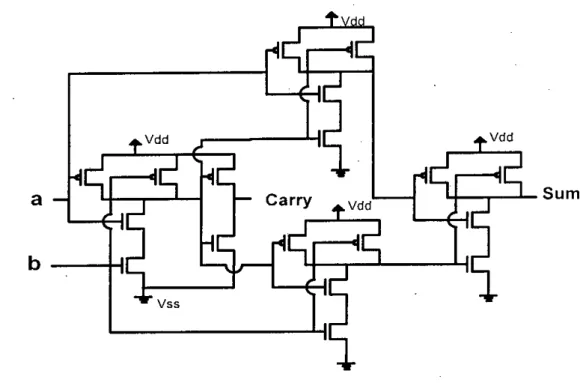
As in an ROF most of the delay occurs in thc Parallel Counter circuit, so emphasis is given to designing the Full and Half Filler circuit. From the HSPICE simulation of the Full Adder circuit the delay to produce the Carry is found to be about 120 ps and the delay to produce the Sum bit is found to be about 260 ps.
Carry
- The Comparator Circuit
- HSPICE Simulation for 5-Input ROF
- Layout Design of the Bit Update Circuit
- Layout Design of the Full Adder
- Layout Design of the Half Adder
- Layout Design of the 3 bit Comparator Circuit
- Layout Design of the 5 input ROF Circuit
- HSPICE Simulation Output from Layout Extraction
- HSPICE Simulation for 5-Input Maximum, Minimum and Median Filter
- HSPICE Simulation for 7-Input Maximum, Minimum and Median Filter
- The Shift Registers
- HSPICE Simulation of the Rank Order Filter with increased throughput
- Conclusion
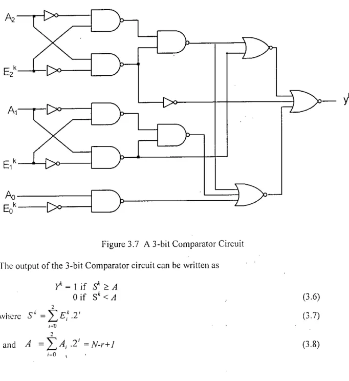
The gate and transistor level diagram of the Half Adder circuit are shown in Figures 6.6 and 6.7 respectively. The transistor-level HSPICE simulation output of the Rank Order Filter is shown in Figure 6.12. The simulation is performed in the O.I 81lm CMOS process for the inputs as shown in Table 2.1. The third smallest element or median of the five input samples should be the output of the ROF.
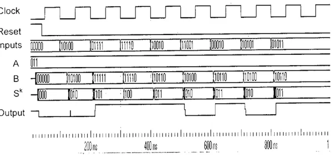
The layout design of the 5-input ROF circuit is shown in Figure 6.17 using the 0.18 11mCMOS process. From the layout of the 5-input Rank Order Filter, the netlist is extracted and HSPICE simulation is performed. The transistor level HSPICE simulation output for the maximum, minimum and median filter as described in Chapter 4 is shown in Figure 6.21.
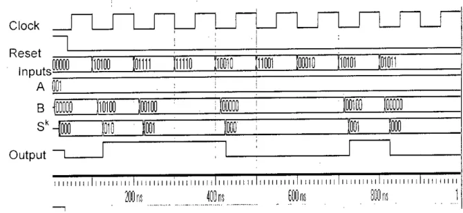
In Figure 6.21, (a)-(e) represent the inputs to the 5-input ROF, and (1), (g), and (h) represent the output of the maximum, minimum, and median filters, respectively. Time 'in} iTIME) Inout Sample number 4. In Figure 6.22, (a)-(g) represent the inputs to the 5-input ROFs, and (h), (i), and U) represent the output of the maximum, minimum, and median filters. . For the inputs shown in Figure 6.25, and for the element rank determined by the r =2 circuit, the output of the modified ROF circuit is shown in Figure 6.26.
Netlist is extracted from the layout design and HSPICE simulation of the extracted data is performed.
CONCLUSION
Concluding Remarks
The throughput of the designed ROF is not satisfactory, although it can operate at a very high clock frequency. However, it is shown in Chapter 5 that if M numbcr Rank Selection circuits are operated in parallel with the data pipe technique using shift registers, the throughput of the circuit can be increased by a factor of M. The HSPICE simulation result of the modified ROF circuit presented in Figure 6.26 is the same as the output shown in Figure 5.3 obtained by the posterior fitting simulation of the VHDL circuit model.
Efforts have been made to design various parts of the ROF with fewer transistors and for more reliable and faster operation. While designing the layout care has been taken that the layout of different parts of the ROF can be easily integrated into a smaller area to form the entire ROF circuit. Interconnect lengths are attempted to be as short as possible to reduce the delay associated with the parasitic capacitance of the interconnects.
It is found that the speed of the ROF circuit from the Layout extraction is 400 MHz, while without the parasitic coupling capacitance it is found to be 500 MHz. The effect of interconnect delay could be reduced by inserting some repeaters in the link path to make the link lines shorter.
Recommendations for future works
If the bit length is M = 8, the desired rank element can be obtained as an output with every 8th clock pulse. In the floor plan design of the ROF. another important thing has been prioritized and that is the interconnect length on the ROF critical path. However, when HSPICE simulates the netlist generated from the ROF layout design extraction, the maximum operating speed of the bc is found to be 400 MHz.
This decrease in operating speed is due to the parasitic capacitance of the long interconnect connections between various parts of the ROF. By using some sort of repeater or regenerator circuit in the path of the long connecting line, the speed of the ROF can be increased. So to measure the performance of the filter, the circuit can be manufactured from any foundry.
Gallagher, Jr., "Threshold Decomposition of Multidimensional Ranked Order Operations," IEEE Transaction on Circuits and Systems, Volume 32, 1985, str. Parhi, "Parallel Processing Architectures for Rank Order and Stack Filters," IEEE Transactions on Signal Processing, Volume 42, maj 1994, str. Chen, "Bit-Serial Realization of a Class of Nonlinear Filters Based on Positive Boolean Functions," IEEE Transactions on Circuits and Systems, zvezek 36, 1989, str.
Leblibici, "Realization of a Programmable Rank- Order Filter Architecture Using Capacitive Threshold Logic Gates", IEEE International Symposium on Circuits and Systems, Orlando, USA, maj 1999, f. Mlynek, "A Compact 31-Input Programinable on Majority Gate Threshold Logic," Proceedings of IEEE International ASIC Conference, 1998,.pp. Leblibici, "A Moduler and Scalable Architecture for the Realization of High-Speed Programmable Rank Order Filters," Proceedings of the IEEE International ASIC/SOC Conference, 1999, pp.
Kuo, "Two Dimensional Order Filter Using Max-Min Classification Network", ISEE Transactions on Circuits and Systems for Video Technology, Volume 8, No.8, December 1998, pp. Broncelet, Jr., "A New VLSI Architecture Suitable for Multidimensional Order Statistics Filtering," IEEE Transactions on Signal Processing, Volume 42, 1994, p.
APPENDIX