In my thesis, I will present two topics of combining electrons in vacuum devices: electron gun, linear accelerator. In the 3D PIC simulations, p/2 standing wave mode field data extracted from 3D time-domain field calculations were injected into a side-coupled LINAC consisting of 25 accelerating and 24 coupling cavities. At the right end of the LINAC, a bunch of electrons with an average energy of 6 MeV escapes from the beam tunnel.
44 3.21 Energy spectrum of electrons calculated with 3D codes and density of emitted electrons at the end of the LINAC waveguide.
Introduction
Electron bunching in vacuum devices
To implement the angle effect on our previous one-dimensional theory, we used the concept of an 'effective' secondary emission energy spectrum in the direction normal to the surface. To the best of our knowledge, the error is acceptably small for a 6 MeV X-band side-coupled cavity waveguide because the field data are compared without any mechanical adaptation of the waveguide to the cavity. Reducing the gap distance to 1 μm, demonstrated by field emission arrays (FEA) [52–55] , appeared to be the best solution to avoid the transit time effect.
In this paper, for the first time to our knowledge, a fully quantitative, theoretical understanding of the transit time effect on the modulation frequency in a vacuum diode is given, together with physical conditions for breaking this limit.
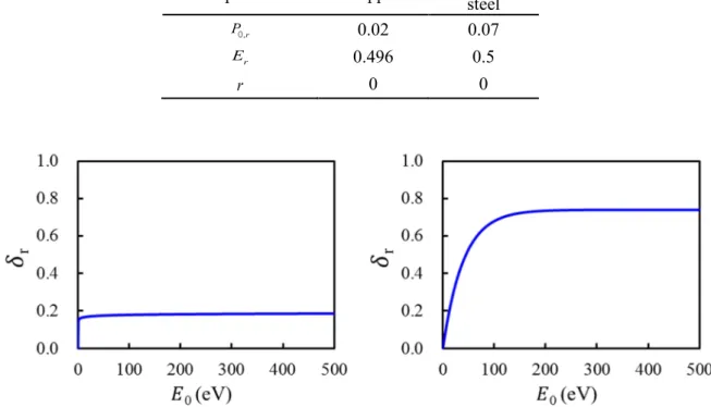
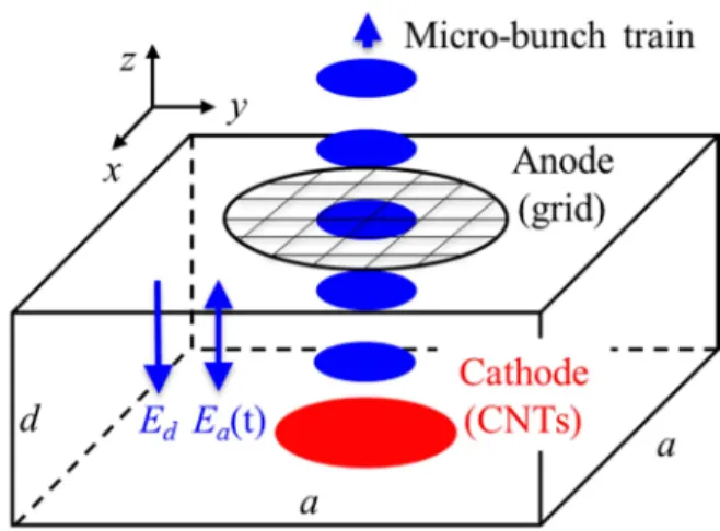
Electron Bunching From a DC-biased Single Surface Multipactor
Introduction
In a real system, the alternating field provides the radio frequency wave in the photonic crystal structure.
Furman-Pivi model
- Fixed point theory
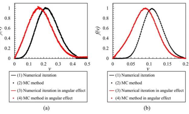
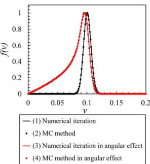
In this section we study the characteristics of the electron beams, including more realistic features of secondary emission. Here the realistic features can be described by two properties, which were not considered in our previous work [1,4]: one is the much broader energy spectrum of the secondary electrons and the other is the non-zero emission angle. In addition, to account for the emission angle effects of the secondary electrons by the one-dimensional map theory, we derived the “effective” emission spectrum of the longitudinal velocity, which was implemented in the map theory in the energy dispersion term.
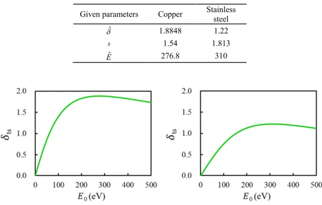
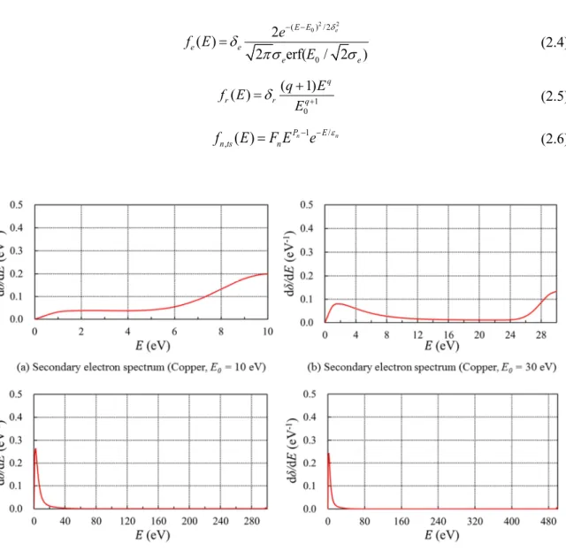
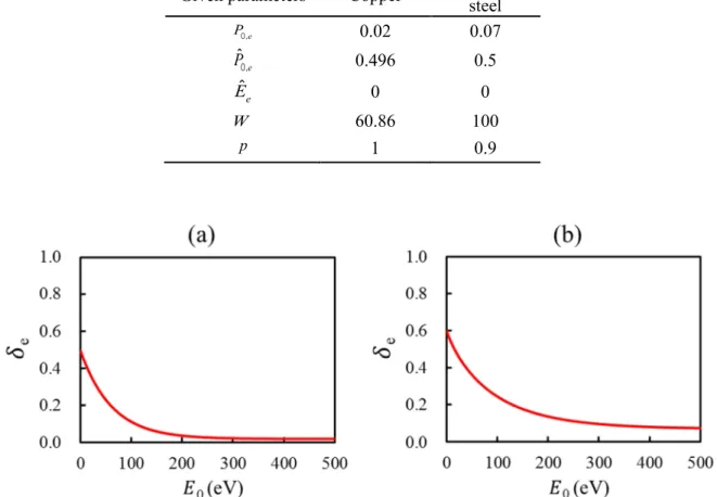
For the realistic energy spectrum and emission angle of the secondary electrons, we used the analytical fitting formulas in the article by Furmann and Pivi [61]. The emission angle and energy variation of the probability distribution can be expressed by: dP E( ,q)=A fn( )E cosq qd dE, where. Here, F( )nz actually means the probability distribution of the velocity in the z-direction, taking into account the effect of the emission angle.
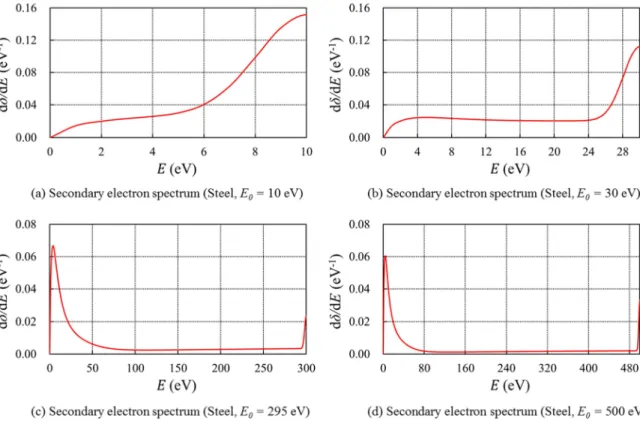
For the PIC simulations, the empirical formulas in Ref [61] were implemented into the secondary electron routine of the code. The secondary emission routine allows a full energy spectrum of the secondary emission, which is composed of backscattering, rediffusion and true secondary electron emission [62]. The width of the material surface was 200 μm in the transverse direction, and the longitudinal length of the system was 200 μm.
To extract the electron bunch phase information from the PIC simulations, we measured the full width at Imax/e of the electric current through the emitter plate as in Figure 2.10, and converted it to the phase following the procedure in Ref. Note that the width of the phase extension is proportional to the longitudinal size of the bundle.
Conclusion
Design of X-band 6MeV side-coupled linear accelerator
Introduction
- Application of LINAC
- Property of LINAC
- Important parameters of LINAC
- Design flow
- Numerical stabilization
- RF breakdown limit for X-band linear accelerator waveguide
- Optimization of linear accelerator
- Electromagnetic simulation for X-band full LINAC cavity waveguide
In the previous chapters, however, we have assumed that the beam is influenced by the cavity, but we have ignored the effect of the beam on the cavity fields. As the jet flux increases, it becomes important to treat the effects of the interaction between the jet and the cavity more carefully. The effects of the beam on the cavity fields in the acceleration mode are referred to as beam loading.
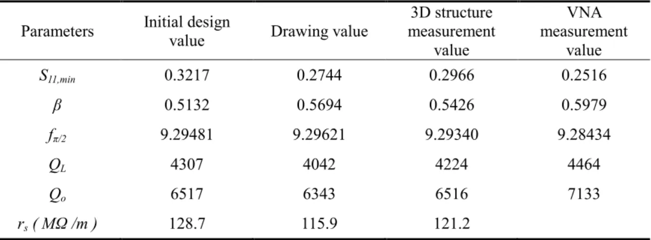
The design process for the X-band (9.3 GHz) 6 MeV LINAC waveguide can be divided into 6 steps. In the first iteration of the steps, the field profiles are given by eigenmode calculations in step 3. By analyzing the physical properties of the accelerated electrons, the validity of the designed values for the cavity waveguide can be verified.
Considering the quality factor (Q) of the desired p/2 mode in the unit cell, we determined the allowable limit for the resonant frequency between each cavity. W Q, where wo is the resonant frequency of the cavity and w is the RF frequency derived from a generator. And the resonant frequency of fsc side coupling cavities can be mainly manipulated by the parameter defined as a.
3.12 (b), where the electric fields are described on the half-section of the unit cell, denoted as no. cells. And the resonance frequency of fsc side coupling cavities can be predominantly manipulated by the parameter defined as sc_gap. The phase of the electric field changes periodically, which coincides with the phase change in the p/2 standing wave mode.
Both the electrons escaping through the beam tunnel with relatively high kinetic energy and the electrons colliding on the beam tunnel or the cavity wall were included in the estimation of the energy transfer.
Cold test
Even if the optimized bead and string are selected and the temperature of the LINAC waveguide is kept constant, there is still a small fluctuation in the data caused by the stepper motor and cooling system. The S-parameter data was collected at the same position 100 times and the average value of the data was chosen while the heel was moved by the stepper motor with each deviation of 0.5 mm. This measurement is based on the fact that a small interfering object, such as a bead, changes the stored energy in the cavity.
When the bead is located between the nozzles of the accelerating cavities, the bead changes the capacitance of the cavity. To directly compare the computational results and the experimental results, the electric field distribution was measured without any mechanical tuning. However, we believe that the discrepancy is quite small because each cavity in the waveguide was not mechanically tuned during fabrication, brazing, and bead pull testing.
To our knowledge, without the mechanical tuning, it is difficult to build clear p/2 standing wave mode in an X-band 6 MeV side-coupled LINAC waveguide. Data” is electric field calculation ( fb n, - fs ) from simulation data where fb n, is the frequency from Sim. Data” is electric field calculation f'b n, - f'er from experimental data where f'b n, is measured frequency of LINAC with string and bead by moving the bead at each cell, f'er is measured frequency of LINAC with string only .
Conclusion
Introduction
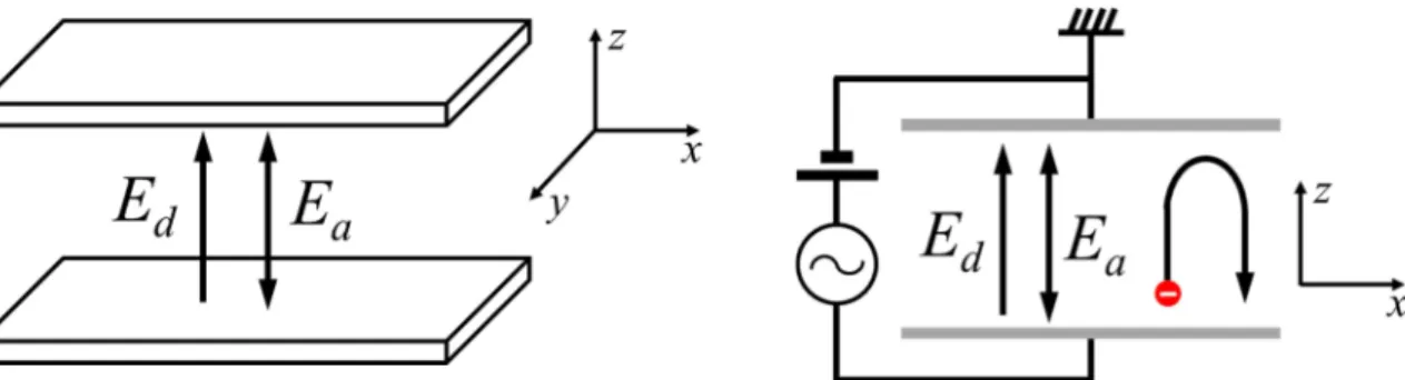
The DC field is set in the negative z-direction between the top and bottom plates of the cavity. For the one-dimensional analysis of this system, the variation of the electric field in the x and y directions over the beam cross-section is neglected. Note that time t in Eq. 4.1) is referred to each electron so that it is emitted at t = 0 and sees the electric field –Easinϕ +Ed at the moment of emission.
Considering that the electron emission occurs in a bundle form as implied by Fig. 4.2, the existence of such a solution to Eq. 4.6) indicates that an electron beam bound together by periodicity 2π/ω can be extracted from the cavity. Consequently, the possibility of generating bundled beams can be exploited by analyzing the behavior of the coefficients A and B. Electrons with < 0.5, which are the other half of the emitted electrons, have a solution to Eq.
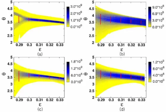
In this case, the range of emitting phase of the electrons escaping the system is significantly limited by the excluded transit phase (ETP). The crossing points around the bottom of the B curve are thus actually excluded from the possible transit phase. The x-coordinate represents the sum of the start phase and the transit phase, + , normalized by 2π, and the y-coordinate represents the beam modulation frequency f normalized by defined in Eq.
The discontinuity of the permitted transit phase in this case can be understood by the ETP described above. Increase of the phase width as approaches −1.0 can be easily deduced because the extreme case = −1.0 means that a continuous DC field is applied to the CNT cathode, which then emits the electrons without any modulation. d) the map of the entire area.
Conclusion
4.6, a very nice microbeam array of emitted electrons is observed, showing the electron current of order 0.1 mA (see the inset), which is a remarkably high current density beam containing a significant space charge force. In principle, even a much larger amount of current can be obtained by using high-order TMmn0 modes [75,76] instead of the fundamental TM110 mode treated here for simplicity. The simulation result confirms our theoretical prediction that the microbeam frequency of vacuum diode electrons can be significantly extended to THz regimes by increasing the gap with a good DC field.
Summary
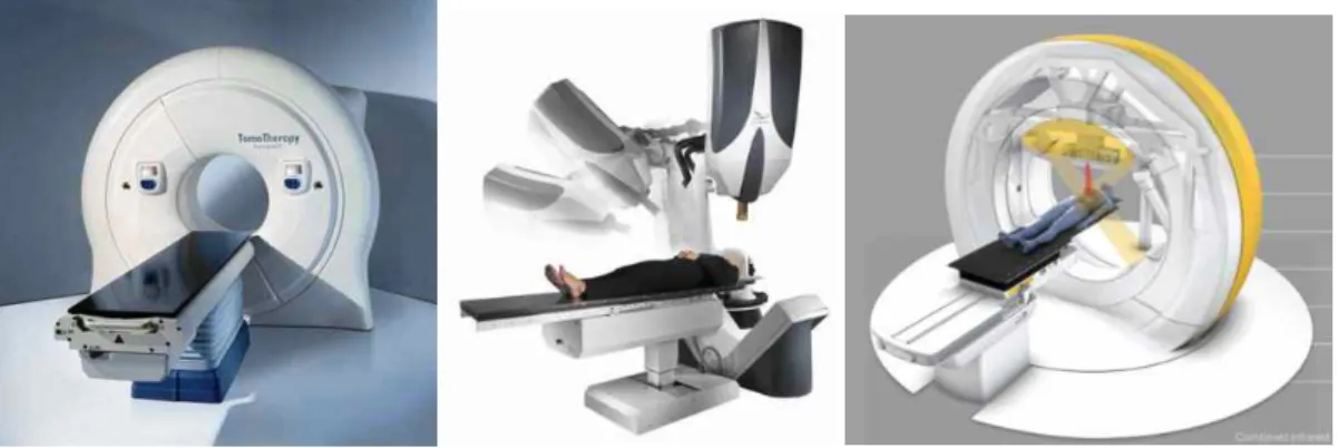
Fujiwara, et al., 950keV, 3.95MeV and 6MeV X-band linacs for non-destructive evaluation and medicine, Nucl. Hirai, et al., Design and experiment of dual-energy X-ray material recognition using a 950keV X-band Linac, Nucl. Kawawda, et al., Development of a four-dimensional image-guided radiotherapy system with a gimbal X-ray head, Int.
Hiraoka, et al., Development of an ultra-small C-band linear accelerator guide for a four-dimensional image-guided radiotherapy system with a gimbal X-ray head, Med Phys. Duchateau, et al., Geometric accuracy of a novel gimbal-based tumor tracking system for radiotherapy, Radiother. Namkung, et al., Design of compact C-band standing wave accelerating structure that improves RF phase focusing, in: Proc.
Fallone, An integrated 6 MV linear accelerator model from an electron gun for dosing in a water tank, Med Phys. Hiraoka, et al., Development of an ultrasmall C-band linear accelerator guide for a four-dimensional image-guided radiation therapy system with a gimbal x-ray head., Med. Palumbo, et al., Design and RF measurements of an X-band accelerating structure for linearizing the longitudinal emittance at SPARC, Nucl.
Joo, et al., High order mode formation of externally coupled hybrid photonic-band-gap cavity, Appl. Bak, et al., High order mode oscillation in a terahertz photonic-band-gap multibeam reflex klystron, Appl.
APPENDIX