LASERS AND DETECTORS Thesis by
Liew-Chuang Chiu
In PartialFulfillment of the Requirements for the degree of
Doctor of Philosophy
CaliforniaInstitute of Technology Pasadena, California
1983
(Submitted May 12, 1983)
Tomy parents
ACKNOWLEDGEMENTS
I would like to express my sincere gratitude to my advisor. Professor Amnon Yariv, for his encouragement and support throughout my graduate studies at Caltech. His keen scientific intuition and extraordinary physical insights have been a constant source of inspiration. It has been aprivilege to be a member of his highly motivated quantum electronics researchgroup.
A special thanks goes to Dr. Shlomo Margalit. who initiated valuable ideas leading to much of the work in this thesis. I am especially thankful to Dr. Tom Koch, who introduced me to the field of quantum electronics and had provided valuable assistance throughout my work. I am also indebted to Dr. Pei-Chuang Chen, Ti-rong Chen, Kit-LaiYu. and John S. Smith, who collaborated in much of the work reported here. I would also like to thank Christopher Harder, Kerry Vahala, Drs. Henry Blauvelt, Abraham Hasson, UzielKoren, and Kam-Yin Lau for their valuable assistance. The invaluable technical assistance of Mr. Desmond Armstrong deserves a note of specialthanks.
Abstract
The subjects of this thesis can be divided into two main categories: III-V sem iconductor lasers and detectors. The first two chapters are concerned with the InGaAsP/InP laser diodes. The final two chapters are related to fundamental problems in the avalanche photodiodes and the new class of quantum well infrared detectors.
The kinetics of themass transport phenomenon in InP is studied experimen
tally. Application of this technique to laser fabrication has resulted in very low threshold terrace mesa lasers.
The continuing problem of the excess temperature sensitivity of InGaAsP lasers and light emitting diodes is studied in detail. Non-radiative Auger recom
bination and electron leakage are found to be important factors affecting the temperature sensitivities of these devices.
Impact ionization in the GaAlSb system is investigated. The resonant nature of the enhanced impact ionization of holes is discussed.Further enhancement is predicted to be possible in quantum well structures.
The new class of quantum well infrared detectors is described. Theoretical considerations on absorption coefficients and otherparameters essential to dev
ice design and performanceare discussed.
-TABLE OF CONTENTS-
Chapter 1 INTRODUCTION 1
Chapter 2 STUDYAND APPLICATION OF THE HASS TRANSPORTPHENOMENON IN InP
2.1 Introduction 4
2.2Mass Transport Process 4
2.3Properties of p-n Junctions "Grown" by MassTransport Process 16 2.4 Application andEffects on LaserPerformance 21
References - Chapter 2 29
Chapter3 TEMPERATURE DEPENDENCEOF THE THRESHOLD CURRENT OF InGaAsP DOUBLE HETEROSTRUCTURE LASERS
3.1 Introduction 30
3.2 InterbandAuger Recombination in InGaAsP 32 3.3Nature of Electron Leakage inInGaAsP/InPDouble
Heterostructures 44
3.4 CarrierLeakagein InGaAsP/InP Heterostructure-Experiment 46 3.5 CarrierLeakagein InGaAsP/InP Heterosturcture-Theory 54 3.6Dependence of To onP-Cladding Layer Doping Level 66 3.7 Auger Recombination in Quantum Well InGaAsPLasers 74
Appendix A Bl
References - Chapter3 B4
Chapter 4 DIPACTIONIZATIONIN ΠI-VSEMICONDUCTOR COMPOUNDS
4.1 Introduction 87
4.2Electron and HoleImpact Ionization Coefficients 90 4.3 Resonant EnhancedHole Impact Ionization in GaAlSb? 95 4.4 Resonant EnhancedHoleImpact Ionizationin Quantum Wells 99
References- Chapter 4 104
Chapter 5 QUANTUM WELL INFRARED DETECTORS
5.1 Introduction 105
5.2Free CarrierAbsorption in GaAs/GaAlAs QuantumWells 105 5.3 Phononless Free CarrierAbsorption in Quantum Wells 107
5.4 IntervalenceBand Absorption 112
5.5 Multi-Quantum-Well Infrared Detector 113
5.6 Proposed Infrared Detector UsingInter-SubbandAbsorption
and Tunneling 118
Appendix B 125
References - Chapter 5 128
Introduction
Semiconductor laser diodes, which emit coherent radiation through stimu lated radiative recombination of electrons and holes in direct gap semiconduc
tor materials, have numerous important applications in communications and consumer electronics. The small size, highefficiency, capability to be modulated directly to the GHz region, and feasibility to be integrated with other semicon
ductor electronic devices make them the most suitable candidates as light sources in optical fiber communication systems. Injection laser diodes employ
ing the quaternary compoundof InGaAsP lattice-matched to InP as active region are capable of emitting in the spectral range of 1.1-1.6 μm. This wavelength range fallsin the region where modern optical fibers exhibit lowloss and negligi ble dispersion. At 1.55 μm, silica fibers with attenuation as low as 0.2 dB/km have been attained. Moreover, the zero dispersion wavelength in single mode fibers can be controlled by a balance between the negative material dispersion and positive waveguide dispersion. As such, the zero dispersion wavelength can be shifted to the desired low loss region. Thus, for long distance high data rate intra- and inter-continental optical fiber communication, the quaternary lasers are the most promising light sources.
For high speed optical fiber communication, reliable lasers with lowthreshold are highly desirable. The buried hetero structure (BH) lasers, with built-in opti
cal and carrier confinements, are attractive candidates for light transmitters in communication links. However, fabrication of conventional BH lasers requires a rather critical regrowth step in an Liquid Phase Epitaxy (LPE) system. As a
result, high yield is difficult to achieve. Chapter 2 discusses the mass transport process and its application tolaser fabrication. This new technique makespossi ble the fabrication of low threshold laserswithout the regrowth step. Section 2.2 describes experiments conducted to study the kinetics of the mass transport process. Section 2.3 studies the properties of p-n junctions ’’grown’' bythe mass transport process, and section 2.4 describes the application of the mass trans
port process in laser fabrication. In particular, the terracemass transport laser and its performance will be described.
Though InGaAsP lasers have been demonstrated to be reliable light sources, a continuing problem plaguing these devices is their excess temperature sensi
tivity. The threshold currents of quaternarylasers are found to be rather sensi
tive to changes in ambient temperature. The temperature sensitivity of the threshold current of InGaAsP lasers is discussed in detail in chapter 3. Section 3.2 studies the interband non-radiative Auger recombination in InGaAsP. Sec tion 3.3 discusses the nature of electron leakage over the InGaAsP/InP hetero
barrier, and the possible relationship between the electron leakage and Auger recombination. In section 3.4, direct experimental evidence of electron leakage is presented. The effects of leakage on the laser threshold is described. Section 3.5 presents a theoretical model for the electron leakage, and calculated results are comparedwith available experimental data. Section 3.6 describes the experi
ments performed to verify some of the theoretical implications. In addition, a new modified laser structure with low temperature sensitivity and threshold will also be described. Finally, in section 3.7, Auger recombination in quantum well lasers is discussed briefly.
In an optical communication link, the performance of the receiver is just as important as that of the transmitter. For long distance optical communication, high speed, low noise detectors with high sensitivity are desirable. An important
class of semiconductor detectors is the Avalanche Photodiodes (APD,s), which operate on the fundamental processes of carrier multiplication through impact ionization. Impact ionization in III-V semiconductors is the subject of chapter 4.
Expressions for the electron and hole impact ionization coefficients in relatively weak fields ( < 105 V∕cm) are derived in section 4.2. Section 4.3 discusses the recently observed "resonant" enhanced hole impact ionization in GaAlSb. The resonant nature of the enhancement is disputed. In section 4.4, further enhancement in hole impact ionization in quantum well GaAlSb detectors is dis
cussed.
Chapter 5is concerned with a new class of infrared semiconductor detectors:
the quantum well infrared detectors. Section 5.2 presents calculations of phonon-assisted free carrier absorption in GaAs/GaAlAs quantum wells. Section 5.3 discusses the possibility of having phononless free carrier absorption in quantum wells, with absoprtion coefficient estimated to be an order of magni
tude larger than the phonon-assisted process. Section 5.4 discusses the inter valence band absorption in quantum wells. In section 5.5, two types of infrared quantum well detectors are proposed, using electron emission from quantum wells and intervalence band absorption respectively. In addition, preliminary experimental results of a detector of the former type will be presented. Finally, section 5.6 discusses the possibility of fabricating improved versions of the detectors usinginter-subband absorption and tunneling in GaAs/GaAlAs hetero junction superlattices.
Chapter 2
Study and Application of the Mass Transport Phenomenon in InP
2.1 Introduction
The recently discovered mass transport phenomenon in InP [2.1,2.2] has gen erated considerable interest. Application of this technique to the fabrication of double heterostructure (DH) InGaAsP lasers has resulted in very low threshold devices [2.2]. For quaternary InGaAsP/InP lasers, this technique eliminates the critical regrowth step necessary in some structures, most notably the buried heterostructure (BH), thereby simplifying the entire fabrication process. The mass transport technique also provides greater flexibility in diode laser fabrica tion. The simplicity of the mass transport process makes it an attractive tech nique in the fabrication of other InP based semiconductor devices and in integrated opto-electronics. The viability of this technique in device fabrication will depend on its consistency and reproducibility. The process has been found to be highly reproducible and quite controllable over the entire wafer. In view of its potential, a better understanding of the process itself would be desirable. In this chapter, a study of the mass transport process is presented. The properties of the resultant mass transport p-n junctions in laser structures are described.
Some advantages and disadvantages of the mass transport technique in laser fabrication and consequent effects on laser performance are also discussed.
2.2 HassTransport Process
The mass transport process refered to in this chapter was first observed by
Liau and Walpole in the fabrication of a heterostructure laser with integrated passive waveguide [2.1]. It was found that when part of a quaternary layer sandwiched between InP layerswas selectively etched away and the wafer heated to about 670 °C in an LPE system in an atmosphere of H2 and PH3, the original air space adjacent to the quaternary layer was filled with InP (see Fig. 1(a) of [2.1] and Figs. 2 of [2.2], or Figs. 2.3(b) and 2.4 in this chapter). Thus, "masses"
of InP have been transported and "grown" on the exposed quaternary material.
This InP mass transport phenomenon should be distinguished from the conven
tional LPE growth of InP, in which the InP is introduced from specially prepared growth solution. This new technique was successfully employed in the fabrica tion of a very low thresholdburied heterostructure laser [2.2] and terrace laser to be described in section 2.4.
However, the origin and kinetics of the mass transport phenomenon thus observed was still unclear. Consequently, a systematic study was conducted to provide information on the origin and dynamics of the mass transport process, and also to probe the characteristics of mass transported InP homojunctions (i.e. p-n junction formed at the interface of the the mass transported InP and the original InP layer) to gain information on the crystalline quality of the mass transported region.
In the original work [2.1,2.2], mass transport of InP was observed in a liquid phase epitaxial (LPE) system in an atmosphere of H2 and PH3. In our case, how
ever, PH3 was not used, and the LPE system was merely flushed with hydrogen.
In most of the cases studied, an InP cover wafer and a thick graphite plate were employed to cover the substrate, which is positioned in a recessed slot on a con
ventional LPE graphite boat. To accomplish the mass transport process, theLPE system was heated to around 675°C and maintained atthat temperature for a period of time depending on the desired experimental conditions and
circumstances.
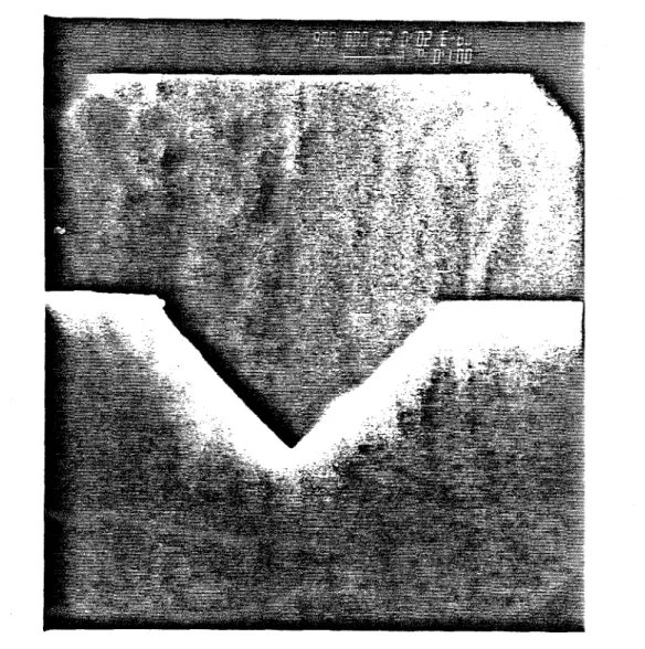
To facilitate the studyof the transport kinetics, U and V shape grooves were etched with iodic acid along the (011) and (011) crystallographic directions respectively on an InP substrate. The width and depth of the U shape groove were ~ 10μm and ~ 4.5μm respectively, and the corresponding values are ~ 5μm and ~ 2.5μm for the V shape groove (Figs. 2.1). After cleaning, the wafers were placed in a shallow slot on a conventional sliding graphite boat and loaded into the LPE system for mass transport. Experiments were performed in the tem
perature range of 670—740 °C and with heating times between fortyminutes and three hours. Figs. 2.1 and 2.2 compare the shapes of the grooves before and after heating. Theshapes of the grooveswere clearly deformed by theheating. In addition to the rounded corners, the depth of the V shape groove was ~.3μm shallower after transport, and the width of the top opening was slightly wider.
The bottom width of the U shape groove was ~ 1.4μm narrower, and the slightly curved bottom became flat after transport. Notice that the convex corners were slightly rounded and materials were clearly "grown”at the concave corners, thus changing the width and depth of thegroove.
A qualitative understanding of themass transport process through the vapor phase could be gained by considering the variation of equilibrium vapor pres sure with the curvature of the solid surface in equilibrium with its vapor. Denot
ing this pressure for a flat surface by P, then the deviation ΔP from P near a curved surface could be expressed as [2.3]
(2.2.1)
where C is a constant, T is the temperature and R the radius of curvature. For a convex surface, R is positive and the equilibrium vapor pressure at the surface exceeds P. Therefore, materials at such places are more prone to be
Figure 2.1(a) SEM picture of the V shape groove before mass transport.
Figure 2.1(b) SEM picture of the U shape groove before mass transport.
Figure 2.2(a) SEM picture of the V shape groove after high temperature (720 °C) mass transport.
Figure 2.2(b) SEM picture of the U shape groove after high temperature (720 °C) mass transport.
Figure 2.2(c) SEM picture of the U shape groove after "low”
temperature (670 °C) mass transport.
evaporated. Conversely, near a concave surface with negative R, the equilibrium vapor pressure is lower and material could be grown. This is consistent with experimental observations of Figs. 2.1 and 2.2 and also Figs. 2.2 of [2.2]. In our experiments, a few tiny In droplets were always found on the surface of the wafer after the transportprocess. This is most probably theresult of the disso
ciation of InP duringthe heating period.
Unfortunately, these observations alone do not eliminate other possible mass transport mechanisms, including the movements of InP molecules over the crys tal surfaces in the solid phase or other solid phase mass migration processes.
However, when a very thin layer of Si3N4 was deposited over the entire substrate, no discernible change in shape was observed after heating. This may indicate that the possibility of solid phase mass migration processes was quite remote.
We recognize that the presence of the Si3N4 layer alters the surface property of the wafer and the above mentioned processes, though unlikely, cannot be posi
tively ruled out.
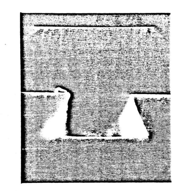
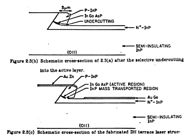
To probe further, two experiments were performed. These employed the ter
race laser structure with a long and narrow etched channel. The terrace was etched either along the (011) or the (011) crystallographic direction. Three epi taxial layers are then grown successively on the etched down portion of the wafer to form a DH laser structure (Fig. 2.3 (a)). The three LPE grown layers are n+-InP cladding layer; undoped InGaAsP active layer; and p-InP cladding layer respectively. Following deposition of a new Si3N4 etching mask on the grown wafer, windows for chemical etching were opened with one side parallel to and approximately 5 μm away from the edge of the original terrace. The p-InP clad ding layer underneath the windows was then removed selectively with a solution of hydrochloric acid and water (1.5 : 1). The quaternary InGaAsP layer was etched next, either with a solution of KOH:K3Fe(CN)6:H2O or H2SO4:Η2O2:H2O,
Figure 2.3(a) Schematic cross-section of the three basic layers of the DH ter racelaser on semi-insulating InPalong the (011) direction.
Figure 2.3(b) Schematic cross-section of 2.3(a) after the selective undercutting into the active layer.
Figtire 2.3(c) Schematic cross-section of the fabricated DH terrace laser struc ture.
resulting in a desired undercuttinginto theInGaAsP activelayer as shown in Fig.
2.3(b). In the first experiment, the substrate and some phosphorous powder were placed in an evacuated ampule (~ 10-6 — 10-7 mm Hg). The mass of the phosphorous powder was estimated to produce a pressure slightly higher than one atmosphere. No mass transport was observed after heating at700°C for an hour. In the second experiment, a substrate and an InP wafer, separated by about 10 cm, were loaded into an evacuated (~ 10-7 mm Hg) ampule. In this experiment, a temperature difference of ~ 30 °C was created along the axis of the ampule between the substrate (at 700 °C) and InP wafer (at 730 °C). After an hour, the InP wafer was decomposed with a drastic change in surface condi tion, but the surface of the substrate remained clean and free from In droplets.
Moreover, mass transport was observed on the substrate and the etched channel was completed filled (as in Fig. S.4(b)). These experiments provided strong sup
port for thevapor phase transportmechanism.
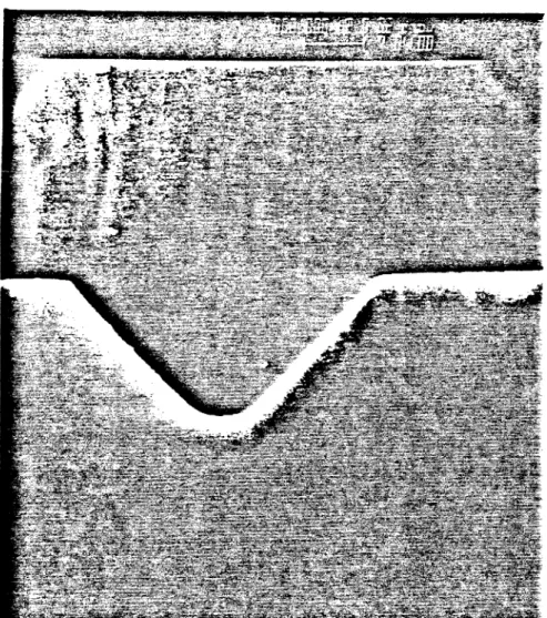
The transport process was found to be a very sensitive function of tempera ture and less sensitive to the duration of heating. Figs. 2.1 consist of SEM pho tographs of the grooves before heating, and Figs. 2.2(a)-(b) show the grooves after heating at 720 °C for three hours, and Fig. 2.2(c) after heating for three hours at 670 °C. In contrast to Fig. 2.2(b), Fig. 2.2(c) shows only minute defor mation in the shape ofthe groove. Conditions for mass transport were also stu
died in the terrace structure described above. After the mass transport pro
cess, a 'burying layer" was "grown" next to the exposed quaternarylayer, giving rise to a buriedlaser structure. Here, besides the temperature and duration, the process also depended on the thickness of the active layer. The width of the transported region was found to vary directly with temperature and duration but inversely with the thickness. Figs. 2.4 show the different widths under two rather different conditions, where the temperature and duration were 675 °C,
F ig u re
2.4SEMp ic tu re s o f
themasstransportedte rr a c e s tr u c tu re : (a )
lower temperatureands h o rt e r
heatingtime;(b)highertemperatureand longerheatingtime.forty five minutes and 740 °C, 1.5 hour for 2.4(a) and 2.4(b) respectively. It can be seen that for lower temperature and shorter heating time, the mass trans port process only occurred in the thin constricted etched region, where the vapor pressure could be higher. From Fig. 2.4(a), it was apparent that in the thin and constricted regions, the mass was transported from regionsadjacent to the quaternary layer. When the wafer was exposed directly to the reducing atmosphere of the LPE system (without the InP cover wafer and graphite plate), mass transport also occurred next to the quaternary layer. However, thermal etching was observed in this case and large In droplets were found on the sur
face of the wafer. In view of this and the results of the experiments conducted in ampules described above, it seems that in the presence of the InP cover wafer and graphite plate, the vapor pressure was automatically adjusted to a condi
tion suitable for mass transport. Moreover, the cover wafer and graphite plate also protect the substrates from problems of thermal etching. Thus, the cover wafer provides a convenient and practical way to obtain reproducible and con
trollable masstransport process.
2.3 Properties of p-n Junctions’Grown'by HassTransportProcess
The properties and quality of ap-n junction areimportant factors influencing the performance of a semiconductor laser. Characteristics and effects of the transported region on laser performance will be described in the following sec
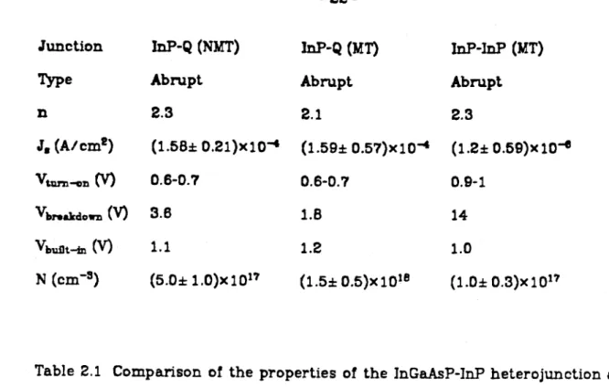
tions. By etching away the quaternary layer completely in the terrace structure, an InP-InP homojunction results after mass transport. These junctions were then compared with the InP-InGaAsP junctions in boththe caseswith (InP-Q MT) and without (InP-Q NMT) a mass transported region grown next to the InGaAsP layer. In each of the three cases, characteristics of 6-8 diodes from the same wafer were measured and an average value was taken. Fig. 2.5 shows the typical
Figure 2.5 Forward I-V characteristics of the diodes.
forward I-V characteristic at low voltages. Assuming the diodes obey the equa
tion
(2.3.1) where J and Js are the current and reverse saturated current densities respec tively, e the electronic charge and V the applied voltage. The values of n and J, were found to be 2.3, (1.2 ±0.59)× 10-6 A/cm2 (InP): 2.1, (1.59± 0.57) × 10-4A/cm2 (InP-Q MT); and 2.3, (1.58 ± 0.21)× 10-4 A/cm2 (InP-Q NMT) respectively for the three cases. The values of n were indicative of generation-recombination domi
nated process. The deviation at higher voltages was due to the effect of the series resistance. In Fig. 2.6 is shown the curve tracer photograph where the difference in turn-on voltages for the hetero- and homojunctions was clearly displayed. The larger turn-on voltage for InP is a direct consequence of the much smaller Js, which in turn is due to the smaller ni (larger bandgap Eg), the intrinsic carrier concentration, of InP as comparedwith InGaAsP.
Fig. 2.7 shows a typical C-V characteristics of the three different types of diodes. The linear relationship of 1/C2 vsV justifies the classification of these as abrupt junctions. From these measurements, values of the built-in voltages (Vbi) and doping concentrations could be extracted.Assuming these to be one-sided abrupt junctions, the doping concentrations in the active layers were estimated to be (1.0 ± 0.3) ×1017cm-3 (InP), (1.5 ±0.5)×1018 cm-3 (InP-Q MT) and (5.0 ± 1.0) ×1017 cm-3 (InP-Q nMT). These values are consistent with the approxi matevalues calculated from the semi-empirical expressionof Sze [2.4]
(3.3.2)
where Eg is the bandgap energy in eV and N the concentration in cm-3. The values of the reverse breakdown voltages were found to be 14 V (InP-InP), 1.8 V
I
Figure 2.6 Curve tracer photograph showing the difference in I-V characteris tics of the hetero- and homojunctions. The homojunction has a larger turn-on voltage.
Figure2.7C-Vcharacteristicsofthediodes.
(InP-Q MT) and 3.6 V (InP-Q NMT). The higher doping concentration in the quaternarylayer afterheating is most probably due to the Zn diffusion from the cladding layer into the quaternary layer when the wafer was heated at around 675 °C during the transport process [2.5]. This has important consequences on the temperature sensitivity of laser thresholds, as will be explained in the next section and further elaborated inchapter 3.
The junction characteristics are summarizedin Table 2.1. TheInP mass tran sport homojunction is indistinguishable from grown junctions, indicating the high crystalline qualityof thetransportedregion.
2.4 ApplicationandEffects on Laser Performance
The mass transport technique has been applied in laser fabrication, resulting in extremely low threshold lasers [2.2]. In the BH structure of [2.2], the other
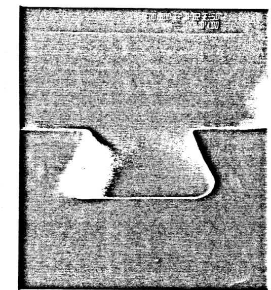
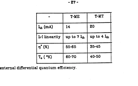
wise necessaryand critical regrowth process is completely eliminated. The mass transport technique can also find application in the fabrication of other devices, such as LED’s and super-luminescent diodes, just to name a few. However, it should be mentioned that the mass transport process can also give rise to undesirable results. For example, in the fabrication of distributed feedback lasers, the corrugation grating on the substrate could be smeared due to the transport process, and special care has to be taken to prevent the transport process [2.6]. In this section, the low threshold terrace mass transport laser (T- MT) will be described and compared with the terrace mesa laser (T-ME) to probe the effects of mass transport on laser performance.
The terrace structure shown in Figs. 2.3 has been processd into low threshold lasers (Fig. 2.3(c)). Fig. 2.4(a) showed theSEM photograph of the cross-section of the T-MT laser. The T-ME’s and T-MT’s were identical in allrespects except that the mass transport step was skipped in the T-ME’s. resulting in active layers
Junction InP-Q (NMT) InP-Q (MT) InP-InP (MT)
Type Abrupt Abrupt Abrupt
n 2.3 2.1 2.3
Js(A/cm2) (1.58 ± 0.21) × 10-4 (1.59±0.57)× 10-4 (1.2± 0.59) × 10-6
Vturn-on (V) 0.6-0.7 0.6-0.7 0.9-1
Vbreakdown (V) 3.6 1.8 14
Vbuilt-in (V) 1.1 1.2 1.0
N (cm-3) (5.0±1.0)× 1017 (1.5± 0.5)×1018 (1.0 ± 0.3) × 1017
Table 2.1 Comparison of the properties of the InGaAsP-InP heterojunction and InP-InP homojunction.
Figure2.8Schematiccross-sectionofthefabricated T-ME laser.
which were not "buried" and were exposed directly to air. Fig. 2.8 shows the schematic drawing of the T-ME laser. Since the only structural difference in these two lasers is the mass transported region in T-MT, theT-MElaser is thus a suitable structure for making a comparative study to investigate the effects of mass transport onlaser performance.
The T-MT lasers with similar dimensions had threshold currents averaging around 20 mA, compared to 14 mA in the case of the air interface T-ME’s. The average L-I characteristics of T-MT’s are linear up to 4 Ith. The corresponding figure for the T-ME’s is 7Ith. Also, the T-ME’s were found to havehigher external quantum efficiencies than the T-MTs (35-45% vs 55-65%). Fig. 2.9 shows the L-I characteristics of typical T-MT and T-ME’s. The far field patterns are shown in Fig. 2.10. Here the scattering from the exposed sidewall of the T-MEs is apparent.
In addition, the T-ME’s were found to be less temperature sensitive. Using the empirical relation for the temperature dependence of threshold current
Ith = I o e ^(T/T o
), (3.4.1)
the To's for the TM-E and T-MT lasers were found to lie in the range of 60-70 °K and40-50 °K respectively. The lower Tos of theT-MT’s could be explained bythe larger electron leakage over the InGaAsP/InP heterobarrier due to lower doping level in the cladding layer as a result of zinc out diffusion during the heating period of the mass transport process. This leads us into the subject of the tem perature dependence of quaternary lasers treated in detail in the next chapter, where further experimental evidence as well as theoretical model calculations provide a coherent interpretation of the difference in To,s of the T-ME and T-MT lasers.
The comparison of the characteristics of the T-MT and T-ME lasers is sum marizedin Table 2.2 It should be stressed that though T-ME lasers appear to be
Figure 2.9 L-I characteristics of typical T-MT and T-ME lasers.
Figure2.10
F a r
field patternsoftheT-MEandT-MTlasers.- T-ME T-MT
Ith (mA) 14 20
L-Ιlinearity up to 7 Ith up to 4 Ith
η°(%) 55-65 35-45
To (°K) 60-70 40-50
*external differential quantum efficiency.
Table 2.2 Comparison of the characteristics of the T-MT and T-ME lasers
superior, the exposed unpassivated InGaAsP surface leads to higher surface scattering loss and an irregular asymmetric far field pattern (Fig. 2.10(a)). More importantly, surface passivation is essential for the long termstability of lasers.
Thus the mass transport process offers an excellent way to passivate the sur
face.
References - Chapter 2
2.1 Z. L. Liau and J. N. Walpole, PaperWB 3, Technical Digest, Topical Meeting on Integrated andGuided WaveOptics, Optical Society of America (1982) 2.2 Z. L Liau and J. N.Walpole, Appl. Phys. Lett.,40,p. 56B (19B2)
2.3 J. W. Cahn, and D. W. Hoffman, ActaMetallurgica, 22 , p. 1205, (1974)
2.4 S. Μ. Sze, "Physics of Semiconductor Devices," Chap. 2, J. Wiley and Sons, New York (1981)
2.5 C. B. Su, J Schlafer, J. Manning, and R. Olshansky, Elect. Lett., 18, p. 595, (19B2)
2.6 K. Utaka, private communication.
Chapter 3
Temperature Dependence of the Threshold Current of InGaAsP Double Hetero structure Lasers
3.1 Introduction
Semiconductor injection lasers using the quaternary compound InGaAsP as active layers generally exhibit threshold current densities that depend strongly on temperature. Empirically, the temperature dependence of the threshold current of all semiconductorlasers can be expressed in the form
Ith = Io e^(T/To) (3.1.1)
where Io is a constant, T is the temperature, and To is a characteristic tempera
ture that measures the temperature sensitivity of the laser. InGaAsP lasers are characterized by a low To ranging from 50-80 °K for temperatures above
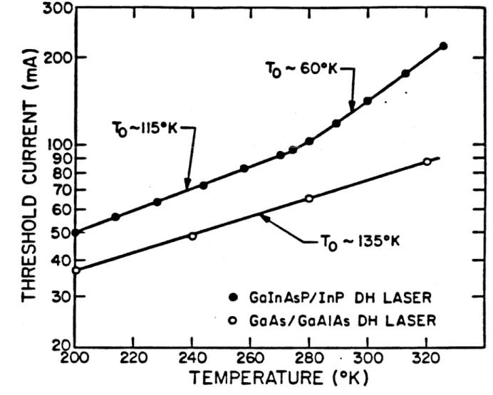
~ 220 °K. This value is considerably lower than that of GaAlAs/GaAs lasers, which is typically greater than 120 °K. A typical plot of In Ith vs T for the GaAlAs/GaAs and InGaAsP/InP systems is shown in Fig. 3.1. For InGaAsP lasers, the temperature beyond which the To drops drastically is termed the "break
point" temperature.
Also, in InGaAsP light emitting diodes (LEDs), the output power saturates at high injection current densities. The excess temperature sensitivity in lasers and severe output power saturation in LEDs remain the two unsolved problems.
The underlying mechanisms in the two cases are believed to be the same. Hith
erto, manymechanisms, including in plane superluminescence [3.1], inter-facial
Figure 3.1 Typical plot of In Ith vs T for the GaAlAs/GaAs and InGaAsP/InP lasers.
recombination [3.2], inter-valence band absorption [3.3], non-radiative recombi
nation via traps [3.4], non-radiative Auger recombination [3.5,3.6,3.7,3.8], and carrier leakage [3.9,3.10,3.11] have been proposed to explain the phenomena.
Among the various mechanisms listed above, the non-radiative Auger recombi
nation and carrier leakage over the heterobarrier are believed to be the dom inating factors. The importance of these two factors will be studied in this chapter.
In the following sections, the non-radiative Auger recombination and carrier leakage will be discussed. Theoretical calculations and models will be compared with experimental results. In addition, Auger recombination in quantum well laserswill also be discussed briefly.
3.2 InterbandAuger Recombination inInGaAsP
It is well known that non-radiative Auger recombination processes become significant in low bandgap semiconductors at high temperatures [3.12,3.13].
Figs. 3.2 show the two dominant Auger processes. In the CHCC process, an elec tron (1) in the conduction band recombines non-radiatively with a hole (1') in the heavy hole band, and the excess energy is imparted to another electron (2) with the appropriate momentum (Fig. 3.2(a)). In the CHSH process, the energy and momentum is taken up by a hole which is excited from the heavy hole band to the split-off hole band (Fig. 3.2(b)).
The theory of Auger recombination in semiconductors was first developed by Beattie and Landsberg [3.12]. The transition probability is obtained from first order perturbation theory by employing Fermi’s Golden Rule with a screened Coulomb interaction Hamiltonian given by
Figure 3.2 The CHCC and CHSH Auger recombinationprocesses. 1.2 and 1', 2' are the initial and final states, respectively.
(3.2.1)
In the above, e is the electronic charge, ε the static dielectric constant,and LD is the screeninglength calculated from
LD-2 = [e2/(εkT)] [2/((2π)3)] ∫ f(k) (1- f(k)) dk
Here, f is the Fermi factor givenby
(3.2.3)
where k is the Boltzman constant, T the temperature, and Ef the Fermi level.
Taking the electronwavefunctions as Bloch states,
where c and v denote conduction and valence band respectively; the matrix ele mentis thengiven by [3.12,3.13]
(3.2.5)
In deriving (3.2.5), the Umklapp processes, which can be shown to be negligible [3.12], have beenneglected. The overlap integrals Fnn, aregiven by
The transition rate can then be expressed as [3.13]
(3.2.7)
In the above, Ei,j are the energies of the particles before and after the interac (3.2.4)
(3.2.6)
tionrespectively, and 2< β<3 due to spin symmetry. The overlap integral |F1F2|2 has been derived using the k∙p method [3.14].For the CHCCprocess [3.14],
(3.2.8)
(3.2.9)
(3.2.10)
(3.2.11)
Here, Eg is the bandgap, Δ the spin-orbit splitting. fcv the oscillator strength, mo the electron mass, ms the split-off hole mass, and Ep is a band parameterrelated to the momentum matrix element [3.15]. Since semiconductor lasers operate under high injection condition which renders the conduction band degenerate, the full Fermi factors (3.2.3) must be used. Unfortunately, use of degenerate statistics renders the analytic integration of (3.2.7)impossible, and therate P is thus calculated numerically assuming parabolic bands. The Auger lifetime is obtained from the expression
where ∆n is the injected carrier density at threshold. It is assumed that the injection level is high, so that ∆n ≈ nth, an excellent assumption for semicon ductor lasers. Data from lasers emitting at 1.1, 1.27, 1.3, and 1.4B μm are taken from references 3.16, 3.5, 3.6, and 3.17 respectively. The band parameters used
and for CHSH process,
with
and
(3.2.12)
in the calculation are listed in Table 3.1. For comparison, the calculated and experimental carrier lifetime at 300 °K are listed in Table 3.2. The total carrier lifetime is obtained fromthe sum of the radiative andAuger effects by
(3.2.13)
The radiative lifetime is obtained byextrapolation of experimental values at low temperatures. As is evident from Table 3.2 and Figs. 3.3-3.6, reasonable agree ment was obtained for lasers with low nominal threshold current densities. For lasers with high nominal current densities, the calculated Auger lifetimes are significantly shorter than the observed values. This is due to the high apparent carrier concentration resulting form the high threshold current density, which indicates the existence of additional loss mechanisms not accounted for here. It shouldbe cautionedthat the Augerlifetime is a rather sensitive function of car
rier concentration as shown in Fig. 3.7, and calculated lifetimes are meaningful only if reliable values of nth are available.
The Auger lifetime is known to vary approximately with the carrier concen
tration as
where a is between 2 and 4. Fig. 3.7 shows the relationship of 1/τ andn for a 1.3 μm. laser at 300 °K. From Fig. 3.7, it is deduced that a = 2.19 for CHCC process and 2.04 for the CHSH process. This compares favorably with the value of 2.2 obtained on LED experiments by Uji et al [3.18]. The apparently slight deviation of a from 2 can be very significant at high injection conditions where n ~ 1018 cm-3. Usually, the Auger process is also expressed in terms of the Auger coefficient C defined as
(3.2.14)
Symbol In1-xGaxAsyP1-y Eg 1.34 - .72y + .12y2
ε XεGaAs + (y - x)εInAs + (1 - y)εInP (mc)/(mo)
0.08 - 0.39y (mh)/(mo)
(1 -y)(.79x + .45(1 -x)) + (.45x + .4(1 -x))y (ms)/(mo)
.17x+ .083(y -x) + .15y
Δ .11 + .421y - .152y2 For lattice matching to InP, x = .4526y/(1 -.031y)
Table 3.1 Band parametersusedin the calculation.
Table 3.2 Comparison of experimental and calculated carrier lifetimes for Wavelength (μm) Jth/d (kA/cm2μm τexp (ns) τcal (ns)
1.1 - 4.0 4.2
1.27 14.0 2.0 1.4
1.3 9.0 2.3 2.0
1.48 7.6 1.7 2.0
InGaAsPlasers at 300 °K.
Figure 3.3 Calculated and measured lifetimes of 1.1 μm laser. Data taken from [3.16].
Figure 3.4 Calculated and measured lifetimes of 1.27 μm laser. Data taken form [3.5].
Figure 3.5 Calculated and measured lifetimes of 1.3 μm laser. Data taken from [3.6].
Figure 3.6 Calculated and measured lifetimes of 1.48 μm laser. Data taken from [3.17].
Figure 3.7 The inverse ofAuger lifetime as a function of carrier concentra
tion for a 1.3 μm InGaAsP laser at 300 °K.
The values of Ccan be obtained from plots like Fig. 3.7.
The results of this section indicate the importance of non-radiative Auger recombination in InGaAsP lasers. However, it should be noted that non-radiative Auger recombination cannot explain the decrease in differential quantum efficiency in theselasers. This indicates the existence of other loss mechanisms.
In the remainder of this chapter, the role played by carrier leakage will be dis
cussed in detail, and the possible relationship between Auger recombination and carrier leakage will be discussed and employed to provide a more complete pic
ture of the mechanisms leading to the low To.
3.3 Nature of Electron Leakagein InGaAsP/InP Double Heterostructures
Recently, the experiments of Yamakoshi et al [3.19,3.20] have demonstrated indirectly that electron leakage over the heterobarrier in InGaAsP LEDs is significant. In their structure, the electrons that leak over the heterobarrier recombine in another 'leak detection" quaternary layer emitting at a shorter wavelength of 1.05 μm. The significant intensity of light at 1.05 μm serves as an indication of electron leakage.
In [3.20], the authors ruled out the non-radiative Auger recombination as the source of electron leakage on the basis that the dominant Auger process is the CHSH process. The end product of such process is an energetic hole and not electron. However, as can be seen from the previous section, the rate of the CHCC and CHSH processes are comparable in the quaternary system. Since the CHCC process creates an energetic electron, it can lead to electron leakage through the hot Auger electrons. It is found that such non-radiative recombina tion could also explain the observation of Yamakoshi's experiments, and the (3.2.15)
nature of the electron leakage should be further investigated.
The total current through the LED can bewritten as [3.18]
(3.3.1)
where n is the electron density. S the area and d the thickness of the active region respectively, and τtot is given by (3.2.13). Therefore,
and
(3.3.2)
(3.3.3)
where IR and Inr denote radiative and non-radiative currents respectively. Since I/eSd is known from [3.20], we obtain the values of n/τtot. A self consistent approach is used to obtain n and τtot. Values of n are varied to calculate the Auger lifetimes for both the CHCC and CHSH processes until the value of n/τtot
agrees with the experimental value of I/eSd. A typical value of 6 nsec [3.18] has been assumed for the radiative lifetime. It is noted that since the 'leak detec
tion" layer is much thicker thanthe 1.3μm layer, the electron concentration in this layer is much smaller. As a result, the Auger lifetime is much longer than the radiative lifetime. Therefore, further electron leakage due to the Auger processes need notbe considered for thislayer.
If all "Auger electrons" leak out, the ratio of the light intensity at 1.3 μm and 1.05 μmwouldsimplybe given by
(3.3.4)
However, not all Auger electrons leak out, and if we assume that only a fraction βdoes leak out, the ratio of intensities becomes
Forthe above to agree with the experimentally measured values of I1.3/I1.05 the requiredβ's have been found to lie between 0.18 and 0.24.In Fig.3.8 and 3.9, the measured intensity ratio as obtained from [3.20] is showntogether withthe cal
culated ratio of τchcc/τrad and τchcc/βτrad, where an average value of 0.22 has been usedfor β throughout. Since a single value of β is sufficient to bring about agreement between experiment and calculation, it gives a good indication that the electron leakage may be intimately related to theAuger process. Note that the CHOC process acts as a generating source of hot carriers, and carrier heat
ing effects may then be important factors governing the current leakage. Evi
dence and a theoretical model of hot carrier enhanced leakage will be treatedin the following sections.
3.4 CarrierLeakage in InGaAsP/InP Heterostructure—Experiment
Although the experiments of Yamakoshi et al [3.19,3.20] have demonstrated that there is significant carrier leakage over the hetero-barrier in 1.3 and 1.5 μm LEDs, the experimental evidence obtained is nevertheless indirect. In con trast, we have fabricated a laser-transistor structure to measure directly the electron and hole leakages over the InGaAsP/InP heterobarrier. The results show quantitatively the existence of a considerable amount of minority carrier leakage in the present laser structure (λ = 1.2μm) and that the leakage tends to increase with the injection current, even beyond the lasing threshold.
A schematic representation of the laser-bipolar-transistor used is shown in Fig. 3.10. The emitter-base junction functions as in an ordinary laser diode. The collector-basejunction is reverse biased, as in a bipolar transistor, to collect the leakage current. The laser part of the transistor is similar to that of a terrace
(3.3.5)
Figure 3.8 Measured and "Calculated" intensity ration I1.3/I1.05 for LED of diameter 100 μm.
Figure 3.9 Measured and "calculated” intensity ration I1.3/I1.05 for LED of diameter 40 μm.
Figure3.10Schematicrepresentationofthelaser-bipolar-transistorstruc ture.
mesa InGaAsP/InP DH laser described in chapter 2. However, an extra N+-InP layer was added in orderto collect the leakage current. The composition andthe thickness of the four epitaxial layers are: N+-InP collector layer (Sn doped, N= 2× 1018 cm-3, 3-4 μm thick), P--InP confining layer (Zn doped, P= 2× 1017cm-3, 1.5 μm thick), undoped InGaAsP active layer (background electron concentra
tion is 4-9 ×1016 cm-3, 0.2 μm thick) and N+-InP confining layer (Sn doped, N= 2 × 1018 cm-3, 4 μm thick). The last three layers constitute a typical DH InGaAsP/InP laser. After epitaxial growth, selective etching was performed on the top N+-InP layer with the resulting mesa structure formed as shown in the left part of Fig. 3.10. In order to have low threshold current lasers, the quater nary layer was undercut with a selective etchant to obtain the desired width.
Part of the wafer was also etched down to the bottom N+-InP layer to facilitate the fabrication of the collector contact as shown in the right part of Fig. 3.10.
Finally, three electrical contacts for the emitter, base and collector of the N-p-N bipolar transistor, were fabricated as shown.
Under forward bias condition, the emitter-base junction acts as a laserdiode.
The electrons are injected from the N+-InP (emitter) into the quaternary (base) region. In this structure, those electrons which have surmounted the hetero
barrier at A and arrived at the base-collector junction (B) will be swept out by the electric field in the reverse biased junction. As the thickness of the P~-InP layer is smaller than a diffusionlength of theelectron (~3-4 μm [3.9]), most of the leaking minority carriers will be collected thus giving rise to the collector current Ic. Since the electron leakage is expected to be much more significant than hole leakage in this system due to the relatively small effective mass of electrons in the active region, the structure shown in Fig. 3.10 is specially designed to measure the electron leakage.
Since the active layer of the laser is bounded on the sides by semi-insulating InP and air respectively, the current leakage due to carriers bypassing the active region through the burying layer, as is the case in some conventional heterostructure lasers, is completely eliminated. This enables us to measure directly the carrier leakage over the hetero-barrier.
The general behavior of the collector current versus the collector voltage is shown in Fig. 3.11. As the collector voltage increases, the collector current also increases and eventually saturates. This saturation occurs when the junction is reverse biased and all the electrons which haveovercome the hetero-barrier are collected. Hence, this saturated collector current is just the electron leakage current (assuming negligible carrier loss in the P--InP layer by recombination process or other processes). It has been found that under low injection condi
tion, the electron leakage is very small. However, it increases rapidly with increasing injection. Forthe present structure, the leakage currentis about 15- 30 percent of the total injection current (with collector disconnected) when the latter is about 20 mA (corresponding to a current density of ~4kA/cm2, which is near the threshold current density of the lasers). A typical leakage current versus the total injection current characteristics is shown in Fig. 3.12. It is noticed that the leakage current increases with injection current and that no saturation occurs even above threshold.
To insure that the current leakage does not flow through the possible parasi
ticjunction nearthe tip of the active layer, the quaternarylayer of some of the lasers was etched away completely. The resulting device was then measured as described above. The results indicate negligible current leakage through this possible parasitic junction.
By reversing the dopant types in Fig. 3.10, hole leakage current can be meas-
Figure 3.11 General behavior of the collector (leakage) current and collector voltage.
Figure 3.12 A typicalleakage current vs injection current characteristics.
ured. However, no hole leakage was detected, even when the injection current was over 10 kA/cm2. We thus conclude that hole leakage is insignificant in InGaAsP/InP heterostructures. The underlying physics will become clear in the next section.
The leakage current as a function of temperature has also been measured in the range of 10-30 °C. Results are shown in Fig. 3.13. It can be seen that the leakage current is a rather sensitive function of temperature. Since the leakage and threshold current can now be measured simultaneously, an intrinsic 'leak
age free" threshold can be obtained by substracting the measured leakage current from the threshold current. Thus, a 'leakage free" characteristic tem
perature To can be obtained. The result is shown in Fig. 3.14. This demonstrates directly the influence of electron leakage on the To of the laser. The leakage free To of 89 °K is still smaller than the corresponding figures for the GaAs lasers.
This is believed to be limited by the non-radiative Auger recombination as explained in section 3.2.
3.5 Carrier Leakage in InGaAsP/InP Heterostructure—Theory
In this section, a theoretical model for the electron leakage is presented. The model takes into account the detail band structure at the InGaAsP/InP inter
face. Calculated results are then compared with available data for lasers and LEDs. The results indicate the important role played by hot carriers (section 3.3).
A most interesting and at first surprising experimental observation of the last section is the continued increase of leakage current with total current above lasing threshold (Fig. 3.12). Leakage model based on diffusion of electrons alone [3.8,3.21] cannot explain the observed phenomenon, as the expected clamping of carrier density above threshold would lead to a constant leakage
Figure 3.13 Measured leakage current in a 1.2 μ laser as a function of total injection current in thetemperature range of 10-32 °C.
Figure3.14MeasuredToandthe'leakagefree"intrinsic
T
'owhentheleakage current issubstracted.current above lasing threshold . However, the observed behavior can be explained by invoking the electric field dominated drift component of electron current in the cladding layer. Anthonyand Schumaker[3.22,3.23] were the first to recognize the significance of this field. However, their theory predicted a linear dependence of leakage current on injection current above threshold (see equation (3) of [3.23]), contrary to the experimental result (Fig. 3.12). The observed result can be explained by a theory analogous to the minority carrier injection in a Schottky diode [3.24], when the band discontinuity at the hetero
junction is taken into account.
Under high injection conditions in double heterostructure InGaAsP LEDs and lasers, if the doping level in the P-InP cladding layer is low, it can easily be shown that there exists a substantial electric field across the InP layer. In such a case, the hole current can be written as
where e is the electric charge, μp the hole mobility, Na the doping level inthe P- InP layer, and E the electric field strength. For simplicity, only the component transverse to the junction plane will be considered. Under conditionswhere the majority of the current across the p-InGaAsP-P-InP interface is due to holes, the ratio of the drift and diffusion components of the electron leakage current at the junction is then given approximately by
(3.5.2)
where L is the thickness of the cladding layer, and is assumed to be small com
pared to the diffusion length of electrons in the P cladding layer, μN theelectron mobility, and DN the electron diffusion constant. Taking μN = 3000 cm2/V-sec, μp = 150 cm2/V-sec. L=1.5μm, DN =77 cm2/sec (at 300 °K), and Na=1017 cm3, it is
(3.5.1)
easily verified that the drift current is larger than the diffusion current when Jp exceeds ~420 A/cm2. Since normal lasers operate at much higher current den sities, it is expected that the drift rather than diffusion current will dominate.
Since the drift (leakage) current increases with the field E, and E increases with Jp (see (3.5.1)), it follows that the leakage current continues to grow with injec
tion current pastthreshold.
Fig. 3.15 shows the band structure (not to scale) at the p-InGaAsP--P-lnP hetero-interface atthermal equilibrium, κ, the fraction of the diffusionpotential (Vd) on the wide-gap side, is givenby [3.25]
(3.5.3)
where εis the dielectric constant and the subscripts 1 and 2 denote the low and high gap materials respectively. The hole current under a forward bias V (= V1 +V2; V2= κV,V1 =(1-κ)V) is then given by (Appendix A)
(3.5.4)
with
(3.5.5)
where
Figure 3.15 Band structure at the p-InGaAsP-P-InP hetero-interface at ther mal equilibrium.
(3.5.6)
which are analogous to the thermionic-diffusion model of a Schottky barrier [3.26]. In the above, m2h is the hole effective mass andΔEv is the discontinuityin the valence band. The electron concentration at x2 (see Fig. 3.15) is given approximately by
s
(3.5.7)
where n1 is the electron density in material 1 (InGaAsP), Ai's areconstantswhich account for the degeneracy [3.25], and NC1 and NC2 are the conduction band effectivedensity of states.
In most cases, it can be verified that Vd >>([kT]/[2m2hπ])½, and the conduction mechanism is dominated by thermionic emission [3.27]. Also, though (3.5.4) indicates a rectifying characteristic, the large value (exceeds 1000 A/cm2 in most cases) renders the junction more "ohmic" thanrectifying in nature.
Solving the carrier transport and continuity equationsfor electrons, the elec tron leakage current is given by [3.24]
where
(3.5.9)
with τN2 the electron lifetimein the InP cladding layer and L the thickness of the cladding layer. In arriving at the above solution, we have assumed the boundary condition of N2(L) = 0. However, when the leakage is drift dominated, the boun daryconditionN2(L) is not importantas is apparent from (3.5.8).
The total injected current density Jtot is simply
(3.5.10) Since Je is just the leakage current Jleak, it follows that the recombination currentJrec = Jp. Up to lasingthreshold, Jp can be expressed as
(3.5.11) where d is the active layer thickness, B the radiative recombination constant, Cchcc and Cchah are the Auger coefficients for the CHCC and CHSH processes (3.2.15). B is estimated from spontaneous lifetime data and Cchcc and Cchah are calculated as described in section 3.2.
As can be seen from (3.5.4), (3.5.5), (3.5.6) and (3.5.7), the discontinuities in the conduction (ΔEc) and valence band (ΔEv) play an important role in deter
mining the magnitude of the leakage current. Unfortunately, the discontinuity in the quaternary system is not known accurately. However, there are experi mental [3.28,3.29] and theoretical [3.30] indications that a substantial fraction of the discontinuity lies in the valence band. We have used ΔEc = ⅓Eg as meas- ured in Refs. [3.28] and [3.29]. If the interface is graded, then the potential
"spike" which is resistive to hole injection would decrease, resulting in less leak- age. Here, an abrupt interfaceis assumed. However, the ratio (ΔEc)/(ΔEv) as well as the
doping level Na2 are varied to provide a quantitative trend and estimate of the leakage current and itseffects.
It was found that for 1.3μm LEDs, if effects of carrier heating and/or Auger enhanced leakage [3.31] were excluded, the predicted leakage using reasonable parameters would be much smaller than the observed values. Much better agreement could be obtained by incorporating carrier heating effect or employ-
ing a boundary condition n2(x2) ~ e^-[(s/4)((hωo)/E)(d2/Lp2)] (where hωo is the optical phonon energy, E is the maximum energy anAuger electron can lose and still be able to surmount the heterobarrier, and Lp is the electron mean free path ) and use the approach in section 3.3. Due to the uncertainty in Lp and the availability of experimental data on carrier heating effect, the former is chosen. The results of Te at 300 °K from Ref. [3.32] have been used and the electron temperatures at various lattice temperatures (TL) are estimated fromthe expression
(3.5.12)
Thus, it is implicitly assumed that the hot carriers are generated by the Auger process.
Results of the calculation are presented in Figs. 3.16-3.19. Fig. 3.16 shows the calculated ratio of Je/Jp in an LED with d = .15 μm, L =.3 μm at various tempera tures under three different injection conditions. The triangles are experimental data from Ref. [3.20]. For ΔEc = ⅓Eg, reasonable agreement can be obtained by taking NA1 = 4.6 × 1017cm-3 and Na2 = 1.4 ×1017 cm-3. The dashed line denotes ratio of Je/Jp when the carrier heating effect has been neglected. Fig. 3.17 shows the calculated effect of doping and discontinuity on the magnitude of leakage
Figure 3.18 Calculated Je/Jp under different injection conditions. Experimental data are from Ref. [2]. The dashed line denotes the result when hot carrier effectis neglected.
Figure 3.17 Calculated electron leakage current versus total injected current for different P-InP doping levels and different discontinuities (ΔEe) in the conduction band.
Figure 3.18 Calculated To for different P-InP doping levels. The To = 86 °K is calculated without electron leakage.
current in a 1.2 μm laser with d=.2 μm and L=1.5 μm. It is apparent that in order to minimizeleakage, the cladding layer could be dopedheavily or agraded junction be grown to smear the "spike" at the interface. There is a slight discon
tinuity in slope at Jth∙ However, for largerleakage currents, the change in slope isverysmall and insignificant. Fig. 3.18. depicts the effectof leakage current on the Toofthe laser. The influence of the P-doping is again conspicuous. Note that the curve for To = 5B and B6 °K agrees with the measured one of Fig. 3.14. Fig.
3.19 shows the measured leakage and the predicted leakage using the present model and that of [3.23] at a temperature of 295 °K. It shouldbe stressed that when the doping level inthe cladding layer is high, the "spike and notch" at the hetero-interface can be "washed out," resulting in reduced leakage current and also different dependence of the leakage current on the total injection current beyondthreshold.
It is also clear from (3.5.8) that the ratio of the hole leakage current to elec- tron leakage current will be on the order of (μp/μN)2. Thus, the hole leakage current will be insignificant, and is consistent with the experimental result of section 3.4. To compare the influence of leakage current in lasers of different emission wavelengths, ratios of Je/Jtot have been calculated for Na1 = 5 × 1017 cm-3, Na2 = 2×1017 cm-3, and ΔEv = ⅓Egat an ambient temperature of 290 °K. The results are summarized in Table 3.3. From the table, we see that leakage current decreases as wavelength increases. This is expected since ΔEc increases with the wavelength, giving rise to better carrier confinement. Also, the importance of carrier heating effect is apparent, especially for deviceswith emission wavelengths beyond 1.3 μm.
Figure 3.19 Measured electron leakage current vs Injection current charac
teristics. The dashed line is the predicted leakage current from Ref. [8], the solid line is that predicted by the present model (the discontinuity in slope atthreshold is almostimperceptible).
Table 3.3 Comparison of Je/Jtot for lasers at 1.2, 1.3, and 1.5 μm with and without carrier heating effect.
- With Hot Carriers Without Hot Carriers
λ 1.2 1.3 1.5 1.2 1.3 1.5
Je/ Jtot 22% 11% 4% 11% 3% 0.4%
3.6 Dependence of To on P-CladdingLayerDoping Level
From the previous section (equation (3.5.8) and Fig. 3.1B), we see that the leakage current decreases at least quadratically as the inverse of the doping level in the cladding layer. Therefore, whenthe doping level in the cladding layer ishigh, the leakage current is reduced, leadingto higherTo (Fig. 3.18).
To substantiate the above, experimental investigations of the effects of P- layer doping level on the inherent To of InGaAsP lasers emitting at 1.2 and 1.3 μm were performed under various conditions. The lasers used in the study are the Terrace MesaLasers (T-ME) described in chapter2. This particular structure was chosen because it was essentially the same structure as that used in the measurement of electron leakage. In the first experiment, the atomicfractions of zinc inthe growthmelt were ~10-5 and ~10-4 respectively. TheTo for the low doping level lasers was found to be 43 ± 5 °K [3.33], with average threshold current density around 5.2 kA/cm2. The external quantum efficiencywas found to be 50-60 % for both facets. Forthe lasers grown with higher zinc concentra tion. the To was 85 ± 5 oK (highest obtained was 90 °K) with threshold current densities averaging around 8.4 kA/cm2. Thus, by increasing the doping level in the growth melt, the To was increased significantly. In doing so, however, we paid the penalty in higher threshold current density and lower quantum efficiency (~
30 % for both facets). This increase in the threshold current density is attri
buted to the out-diffusion of Zn from the cladding into the active layer during crystal growth [3.9,3.34].
In the second experiment, a grown wafer with moderate P-doping in the clad
ding layer wascleaved into two structurallyidentical pieces, one ofwhich was re introduced into the liquid phase epitaxy (LPE) system and heated to 675 °C in an atmosphere of H2 for about an hour. Thetwo wafers were then processed into
the T-ME lasers. The To of the lasers from the unheated wafer was found to be 60 ± 7 °K, whereas To was 41 ± 7°K for the lasers fabricated from the heat treated wafer. No significant difference in threshold current was observed inthis case. The phenomenon agrees with the previously observed To of the mass tran sport lasers (To = 40-50 °K) and that of theT-ME's (To = 60-70 °K) (chapter 2.). The decrease in To is attributed to the decrease in doping concentration in the cladding layeras aresult of Zn out-diffusion duringheating.
Having identified the cause of the low To, we proceeded to modify the struc
ture to impede zinc diffusion into the active region. The schematic of the new structure is shownin Fig. 3.20. A thin (0.3-0.5 μm) P--InPlayer was first grown adjacent to the active layer, followed by the ordinary P+-InP high doping layer.
This thin layer acts as a buffer to absorb the Zn diffused from the P+ layer to provide the desirable highly doped cladding layer, and at the same time acts as a "diffusion stop" layer to reduce the Zn diffusion into the active layer.
Theresulting lasers were found to have To of 83 ± 4 °Kwith threshold current densities around 4.0 kA/cm2 (lowest Ith was 11 mA for a cavity volume of 250 ×0.2× 1.5μm3). The light versus current characteristics of a typical laser with threshold current around 20 mAare shown in Fig. 3.21. The external quan
tum efficiencyis around 70 %for bothfacets (at I = 3Ith) and the laser is capable of operating in the fundamental transverse mode and of delivering 200 mW per facet (pulsed operation) at an injection current of 1.8 A. Results of our experi
mental investigations are summarized in Table 3.4. It should be stressed that this simple modification scheme can be applied to most laser structures, result
ing in improved laser performance. The To's measured in the T-ME’s are
"inherent" values, and the modification scheme demonstrated here provides a simple way to improve the temperature sensitivities without sacrificing laser threshold. We also recognize that if the cladding layer is doped with elements
Figure3.20Schematicdrawingofthemodified T-MElaserstructure.
Figure 3.21 Typical light versus current characteristics of the modified T-ME lasers.
Table 3.4 Summary of the experimental observations of To and threshold current density under the various conditions.
Wavelength (μm) Condition To (°K) Jth (kA/cm2) 1.2 Waferheatedat 675 °C 41 ± 7 ~5
1.2 Wafernot heated 60 ± 7 ~5
1.3 Low doping level 43 ± 5 5.2
1.3 High doping level 85 ± 5 8.4
1.3 Modified structure 83 ± 4 4.0
(e.g. Cd and Mg) which do not diffuse into the active layer, low threshold and high To lasers maybe obtained without the present blocking layer.
As a short summary, we have learnedthat non-radiative Auger recombination and carrier leakage are important factors determining the temperature sensi tivity of InGaAsP lasers and LEDs. However, there is an important difference between the two effects. The interband Auger recombination is material depen
dentand intrinsic, and thus unavoidable.However, the carrier leakage is extrin sic and can be reduced by increasing the doping level in the cladding layer, as demonstrated inthemodifiedstructure.
3.7 AugerRecombination in QuantumWell InGaAsP Lasers
Although it has been demonstrated that GaAlAs/GaAs quantum-well lasers exhibit higher To's than normal DH lasers [3.35], it is unclear whether InGaAsP quantum-well lasers would be free from a break-point in the threshold current vs temperature characteristics. In this section, the non-radiative CHCC Auger process in the quantum-well lasers is investigated. It is found that the rate of the CHCC process isgreatly reduced in such quasi two dimensional structures.
Equation (3.2.7) has been modified (see (3.7.2)) to calculate the rate of Auger recombination in a quantum-well structure. It is well-known that when the active layer thickness Lz of a semiconductor laser is of the order of the carrier de Broglie wavelength, quantum size effects arise [3.36]. The non-radiative band-to-band Auger process then changes in a fundamental way. For a quasi two dimensional layer, it is usually assumed that the single-particle Hamiltonian can be separated into a quantized component normal to the layer and continu
ous components in the plane of the layer [3.37]. In such case, the energy spec
trum is given by [3.38]
(3.7.1)
where n denotes the nth quantized state of ks, m* is the effective mass of elec trons or holes, and kx, ky arethe continuous components of the crystal momen tum. The effective masses of the electrons and holes in the direction perpendic
ular and parallel to the plane of the layer have been taken to be the same. The Auger rate for such quasitwo dimensional systems becomes
(3.7.2)
where S denotes summing over discrete states and integrating over continuous states.
In this section, all the calculations have been performed forIn.72Ga.28As.60P.40 for which the emission wavelength is about 1.3 μm. The quantum-well is assumed to be a finite square well and the summation is extended only over the confined states in equation (3.7.2). The small Fermi factors at the top of well (~10-5-10-6) justify this approximation. The rate is then calculated numeri cally and the Auger lifetime is obtained from (3.2.12).
Theresults of the calculation are presented in Figs. 3.22-3.24. In Fig. 3.22, 1/τA
is plotted against the electron density at a temperature of 300 °K and for a quantum-well with width 100 Å. The slope of 2.45 (> 2) is typical of the non- radiative process in degenerate materials. In Fig. 3.23, the non-radiative Auger lifetimes of the quantum-well and ordinary laser structures are compared under the sameinjection conditions and temperatures. Awell withwidth 100 Å has also been assumed. It shows that the Auger lifetime is about two orders of
Figure 3.22 The inverse of Auger lifetime as a function of carrier concentra
tion for a 1.3 μm quantum-well (width= 100 Å) InGaAsP laser at 300 oK.
Figure 3.23 Comparison of calculated Auger lifetimes for a 1.3 μm quantum
veil (width = 100 Å) and ordinaryInGaAsP lasers under the exact sameinjection conditions.
Figure 3.24. Calculated Auger lifetime for a 1.3 μm quantum-well laser as a function of well width at 300oK.