57 Figure 4.6 Cross-sectional view of optical electric field power density (W/m2) at 516 nm wavelength for CdTe (a) Bare PSC, (b) PSC with forward scatterer, and (c) NW SC with forward scatterer. 59 Figure 4.8 Cross-sectional view of optical electric field power density (W/m2) at 516 nm wavelength for CZTS (a) Bare PSC, (b) PSC with forward scatterer, and (c) NW SC with forward scatterer.
Motivation
In addition, a brief overview of the successful implementations of forward scatterers for NW SCs will be presented. Optimizing the absorption of solar energy in solar cells is the first step to achieve improved PCE.
![Figure 1.1 Energy mix of various countries in 2020 [3].](https://thumb-ap.123doks.com/thumbv2/filepdfnet/10824588.0/16.918.170.764.634.1004/figure-1-1-energy-mix-various-countries-2020.webp)
Evolution of Solar Cells
However, due to the vacuum operations and high temperature treatments, the energy required to manufacture these solar cells is still significant. Solar cells made of nanocrystals, organic solar cells [39], perovskite solar cells and quantum dot solar cells [42], polymer-based solar cells and various tandem cells fall under this category[43].
![Figure 1.2 Reported timeline of solar cell energy conversion efficiencies since 1976 [12]](https://thumb-ap.123doks.com/thumbv2/filepdfnet/10824588.0/19.918.164.811.253.592/figure-reported-timeline-solar-cell-energy-conversion-efficiencies.webp)
Emergence of Nanowire Solar Cells
Thin-film solar cells have become popular due to lower production costs compared to 1st generation cells and lower material requirements, making them highly suitable for commercialization. On the other hand, axial-junction solar cells based on these materials have not yet been thoroughly investigated.
![Figure 1.3 Fabrication steps and SEM image of silicon nanowire solar cell [54].](https://thumb-ap.123doks.com/thumbv2/filepdfnet/10824588.0/21.918.171.778.357.641/figure-fabrication-steps-sem-image-silicon-nanowire-solar.webp)
Objectives of the Thesis
Therefore, the use of these materials for axially coupled nanowire solar cells represents a promising field of study, which is the main motive of this thesis. To compare and analyze the performance of forward scattering enabled nanowire solar cells relative to their planar counterparts.
Thesis Overview
This section also presents a brief overview of the studied materials and the categorization and performance of nanowire solar cells. In addition, the electrical J-V characteristics of the solar cells and the improvement of the energy conversion efficiency values were demonstrated.
Scattering of Light by Nanostructures
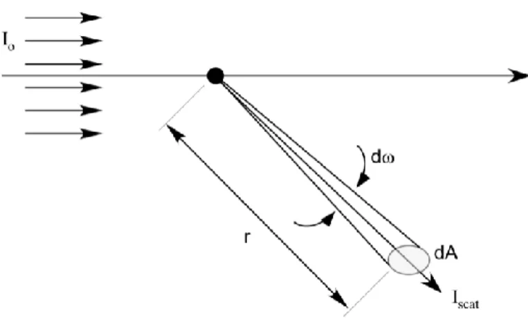
Light Scattering by Spherical Nanoparticles
The scattering cross section is proportional to 6, while the absorption cross section is proportional to 3. The particle extinction cross section is determined by the decrease in incident wave intensity, which is related to the scattering amplitude in the forward direction ( = 0°).
![Figure 2.2 Coordinate geometry for Rayleigh and Mie scattering. b Geometry for Rayleigh scattering; "bench-top" view with y-z as the horizontal plane [108]](https://thumb-ap.123doks.com/thumbv2/filepdfnet/10824588.0/30.918.312.684.166.517/coordinate-geometry-rayleigh-scattering-geometry-rayleigh-scattering-horizontal.webp)
Scattering from nanowires
ᵋ is the intensity of the TE mode of the scattered radiation for the same incident radiation of the TM mode. When the incident radiation of unit intensity is of TE mode, the TM and TE modes of the scattered radiation are given by ᵋ and ᵋ, respectively. ᵊ( )(ᵯ) (2.41) The following extinction efficiencies per unit cross-sectional area of the incident beam is obtained using the extinction theorem.
From these equations, the scattering cross sections via integration are overall values of the angle ᵲ, and this leads to. ᵉ + 1 cos (ᵲ) (2.53) From equation (2.53) it is clear that the intensity of the scattered radiation varies as the fourth power of the cylinder radius and inversely as the cube of the wavelength.
Difference between Mie scattering and Plasmonics
When the cylinder's diameter is small enough compared to the wavelength, the Bessel functions can be expanded into scattering coefficients, and the scattering coefficients can be expressed in powers of ᵯ leading to the following efficiency and intensity and efficiency expressions. These resonances are well defined when the refractive index of dielectric material is high enough (usually >2), and they can be used to control light at the nanoscale in the same way that plasmonic particles can. It should therefore be expected that optimal scattering will occur around 150nm-250nm diameter for the nanowires, and the diameter of the ITO forward scatterer will be larger than that of the nanowire.
Resonance occurs in metallic nanoparticles due to oscillations of free electrons prone to ohmic losses, which can be significant at optical frequencies. The resonances can be achieved without loss if the dielectric shows transparency at the resonance wavelength.
Solar cell Fundamentals
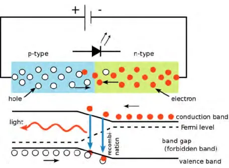
Basics of Photovoltaic Energy Conversion
Absorption of a photon by a solar cell results in the excitation of a valence electron into the conduction band due to the transfer of photon energy. If the photoproduced electron-hole pairs are blocked from leaving the solar cell and accumulating, the amount of electrons on the n-side and holes on the p-side increases. This accumulation of charge produces an electric field at the junction, which reduces the net electric field as it opposes the built-in electric field of the junction.
The diffusion current increases when the electric field opposes charge carrier diffusion across the junction. A new equilibrium state is reached where a voltage is produced across the p-n junction and the output current of the solar cell is equal to the difference between the light-generated photocurrent and the forward bias current.
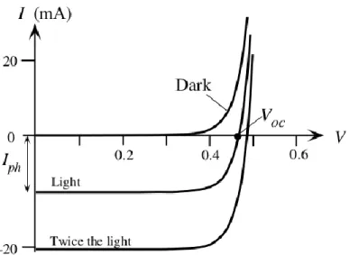
Quantifying Parameters of Solar Cell
The device fill factor (FF) is a performance parameter to find out how close the MPP is to Voc and Isc. ᵋ ᵘ (2.58), where Imp and Vmp are respectively the current and voltage at the maximum power point.
Material Considerations for solar cells
At laboratory scale, CIGS solar cells outperform silicon solar cells; however, their module efficiency still lags behind silicon [97]. They also do not have the toxicity associated with cadmium; therefore, research into kesterite solar cells is gaining traction [118]. However, their efficiency lags far behind the thin-film solar cells using CdTe or CIGS [91].
The high absorption coefficients of CdTe, CIGS and CZTS make it clear that they make excellent absorber layers for solar cells;.
![Figure 2.9 Absorption coefficients vs. photon energy for several solar cell absorber materials [42]](https://thumb-ap.123doks.com/thumbv2/filepdfnet/10824588.0/48.918.317.657.655.988/figure-absorption-coefficients-photon-energy-solar-absorber-materials.webp)
Nanowire solar cell Operation
Despite the recent rise in popularity of nanowire solar cells, they are unlikely to exceed the efficiency limits of planar PV devices even in their best configuration. Heat loss or carrier relaxation due to thermal energy is the second largest loss mechanism in any photovoltaic device, and typically between 30% and 40%. Nanowires have the ability to close this miscibility gap due to enhanced strain relaxation, allowing the synthesis of material with optimal band gaps [126].
Thus, nanowires unleash the chances of making solar cells from undoped materials, thereby eliminating various losses associated with doping [4]. Furthermore, significant cost savings in the fabrication of high-performance multi-junction solar cells by eliminating the need for an expensive grid-matched substrate can be brought about by nanowires.
![Figure 2.11 Nanowire solar cell classification [83].](https://thumb-ap.123doks.com/thumbv2/filepdfnet/10824588.0/50.918.200.779.147.414/figure-2-11-nanowire-solar-cell-classification-83.webp)
Solar cell structure
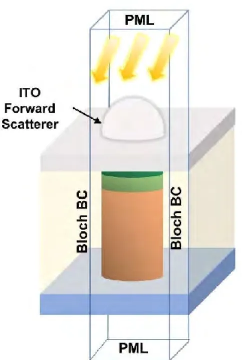
Regarding the experimental viability of the proposed design, fabrication of GaAs and InP axial junction NW SCs with hemispherical ITO particles as forward scatterers has been previously demonstrated.
![Figure 3.1 Device structures of (a) CdTe [131], [132], (b) CIGS [30]–[32], [133], and (c) CZTS [134] solar cells](https://thumb-ap.123doks.com/thumbv2/filepdfnet/10824588.0/54.918.184.792.217.858/figure-device-structures-cdte-cigs-czts-solar-cells.webp)
Optical Simulation Model
Finite Difference Time Domain Model
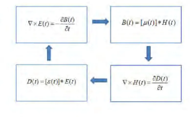
Here, ᵇ is the optical electric field inside the structure, ᵆ is the displacement vector, ᵊ is the magnetic field intensity, ᵳ is the angular velocity, ᵰ is the permittivity of free space, and ᵰ is the relative permittivity of the material in question ( ᵰ = ᵰ ᵰ Yee's technique is also included in the commercial electromagnetic simulator we used in our research, it was set up in such a way that each E-field vector component is in the middle of two H-field vector components.
This technique of solving Maxwell's equation is used in the FDTD solver used in this study for the optical simulation. ᵋ is the AM 1.5G standard solar radiation and ᵰ represents the wavelength corresponding to the band gap of the absorber material above which absorption in the solar cell is negligible.
Boundary Condition
The basic idea of the perfectly matched layer (PML) technique is to add an additional lossy layer around the simulation region with internal impedance matched to the media in the outermost simulation region, ensuring zero reflection from interfaces and soften the pitch as it spreads through the media. . Before the field intensity reaches the simulation limit, it is ensured that it will be attenuated to zero. In our simulation, the PML boundary condition is used at the boundaries perpendicular to the source.
The entire response of a periodic structure can be deduced from the simulation results of just one unit cell in FDTD simulations. When the structure is periodic, but the EM field has a phase change between each period, this boundary condition is required.
Electrical Simulation Model
Both normal and obliquely incident sunlight have been explored in our simulation; therefore, periodic and Bloch boundary conditions were applied in respective cases. To find the electric field, we need to determine the solutions of the following poison equation. The result of the solved equations can have both a steady state and time-varying form.
In the case of analyzing the behavior of the system at a fixed operating state, steady-state simulations are important. By enforcing the = condition in the continuity equations, the carrier density and electrostatic potential can be solved at steady-state.
Model Verification
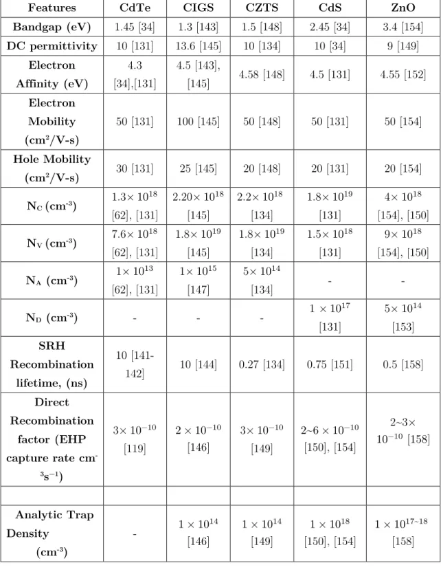
The dimensions of the forward scatterer and the nanopillars are optimized to maximize the optical absorption in the solar cells. The effects of these optimizations on the optical and electrical parameters are reported in this section. The optimum sizes of hemispheres and nanopillars for different absorbers in terms of radius (r) and height (p, the shortest distance between adjacent hemispheres or nanopillars) are shown in Table 4.1, along with the corresponding absorption enhancement values.
Optical Enhancement Analysis
- Planar Solar Cell with Forward Scatterer
- Nanowire Solar cell
- Nanowire Solar cell with Forward Scatterer
- Wavelength Dependence of Absorption Enhancement
- Scattered Field and Generation Rate Profile
- Absorption Enhancement and Oblique Irradiance
- Analysis of Electrical Performance
A maximum of 21.4% coupled absorption enhancement is found for forward-scattering CdTe NW SCs (Figure 4.3(a)) at a dimension (r = 100 nm and p = 50 nm) that coincides with the dimension for maximum enhancement of CdTe NW SC bare (Figure 4.2 (a)). For CdTe, the highest EHP generation is below the center of the forward scattering hemisphere in the planar cell (Figure 4.9(b)) or in the center of the SC NW (Figures 4.9(c) and 4.9(d)). In the case of CZTS, a 5-fold improvement is found in the maximum generation rate for NW SC (Figure 4.11(c)).
The two peaks in the generation rate of CZTS PSC with forward scatter are due to the CdS absorber layer, which becomes significant for CZTS solar cell in the presence of forward scatter (Figure 4.11(b)). For the nanopills, the light is slightly concentrated at the edge instead of the center of the nanopills (Figure 4.13(c) and 4.13(d)).
Conclusion
This chapter provides a summary of the entire thesis and suggests some exploitable prospects related to it that could be the subject of further investigation. For both planar cells and nanowire cells, CdTe showed maximum absorption enhancement values of 8.8% and 21.4%, respectively, due to the use of forward scatterers. The effect of oblique radiation on optical absorption due to the variation of the incident angle of the source was also demonstrated.
The nanowires maintain the absorption enhancement throughout the entire range of angles, with significantly improved optical absorption up to 30°. Consequently, these NW SCs can be implemented in practical conditions to utilize most of the solar radiation during the day.
Suggestions for Future Works
Zeng et al., "Demonstration of enhanced absorption in Si thin film solar cells with textured photonic crystal back reflector," Applied Physics Letters, vol. Ramanujam et al., “Flexible CIGS, CdTe, and a-Si:H thin-film solar cells: A review,” Progress in Materials Science, vol. Krogstrup et al., “Single-nanowire solar cells beyond the Shockley-Queisser limit,” Nature Photonics, vol.
Espinet-Gonzalez et al., "Nanowire Solar Cells: A New Radiation Hard PV Technology for Space Applications," IEEE Journal of Photovoltaics, vol. Ma et al., "Improved Power Conversion Efficiency of Silicon Nanowire Solar Cells Based on Transition Metal Oxides," Solar Energy Materials and Solar Cells, vol.
![Figure 1.4 (a) Schematic of cross-sectional view, and (b) Scanning electron micrograph plan view of the first silicon nanowire solar cell [51].](https://thumb-ap.123doks.com/thumbv2/filepdfnet/10824588.0/22.918.333.658.427.851/figure-schematic-sectional-scanning-electron-micrograph-silicon-nanowire.webp)
![Figure 1.5 Schematic diagrams of the fabrication process of Axial junction Si nanowire solar cells with 12.7% efficiency [89]](https://thumb-ap.123doks.com/thumbv2/filepdfnet/10824588.0/23.918.169.809.518.856/figure-schematic-diagrams-fabrication-process-junction-nanowire-efficiency.webp)
![Figure 1.6 (a) SEM image, (b) Schematic image and (C) Macroscopic image of Axial junction InP nanowire solar cell with 17.8% efficiency [20]](https://thumb-ap.123doks.com/thumbv2/filepdfnet/10824588.0/24.918.243.731.314.495/figure-image-schematic-macroscopic-axial-junction-nanowire-efficiency.webp)
![Figure 2.4 Coordinate system used to represent the scattering by a cylinder with radius a [106]](https://thumb-ap.123doks.com/thumbv2/filepdfnet/10824588.0/37.918.304.670.241.590/figure-coordinate-used-represent-scattering-cylinder-radius-106.webp)
