DOI: 10.12928/TELKOMNIKA.v12i2.2089 419
Planar Finger-Shaped Antenna Used in Ultra-Wideband
Wireless Systems
Rashid A. Fayadh1, Mohd Fareq A. Malek2, Hilal A. Fadhil1, Fwen Hoon Wee1
1
School of Computer and Communication Engineering, Universiti Malaysia Perlis (UniMAP), 02000 Arau, Perlis, Malaysia
2
School of Electrical Systems Engineering, Universiti Malaysia Perlis (UniMAP), 02600 Arau, Perlis, Malaysia
*Corresponding author, e-mail: [email protected], [email protected], [email protected], [email protected]
Abstract
Recently, extensive requirements have developed for ultra-wideband (UWB) technology that provides high activity and small size for use in small communication systems, remote sensing, and radar applications. Thus, we concentrated with high-resolution radar UWB antenna to cover Federal Communication Commission’s (FCC) standard UWB range (3.1-10.6 GHz). The proposed ideal-size and low-cost finger-shaped patch antenna of 24 mm x 19 mm printed on 40 mm x 35 mm rectangular Taconic TLY-5 material was designed and established through experiments and simulations. Results show that the two cut notches of 1.5 mm x 2 mm at the bottom corners of the patch can increase the bandwidth. To increase the radiation area and achieve more resonance frequencies, two cut slots at the top edge of the patch were designed in depth of 10 mm. Four parameters were considered in the analysis of the proposed antenna design, namely the feeder width, number of slots, number of notches, and feed gap space. The simulated and measured results of the main antenna parameters make the design suitable in applications of UWB wireless systems.
Keywords: two notches finger-shaped patch antenna, reflection coefficients, omni-directional patterns, antenna parameters
1. Introduction
was made of FR4 material; a four-filter antenna with three split resonators that was suggested to offer dual band WiMAX and WLAN applications [14, 15, 16], while a CPU-fed, planar, inverted-cone antenna was fabricated to cover the bandwidth from 1.3 to 11 GHz with maximum gain [17]. In order to reduce the cost of antennas and also for reducing the cost, antenna was designed in [18] with substrate made of textile material that used to produce jeans, in addition the patch and the ground plane were made of copper to be suitable for UWB bandwidth. A tuning fork type was proposed and simulated by [19] for operating frequency range of 3.7 GHz to 13.8 GHz with printed patch antenna on a FR4 substrate.
In this paper, we concentrated on the design of ultra wideband rectangular patch with two notches on each bottom side of the patch to achieve the bandwidth around 3 GHz to 12 GHz. The antenna had three slots to extend the radiating element reasonably over the operating band 3 - 12 GHz, which is sufficient for UWB operation. The proposed antenna is smaller in size compared with the previous designs to be suitable for small UWB communication systems. In Section 2, detailed design and the dimensions are presented and followed by Section 3 of fabricated antenna design. After that simulated and measured results with their discussions and conclusions are presented in Sections 4 and 5, respectively.
2. Configuration of the Proposed Antenna
The small size and easy to fabricate antennas are two features strongly desired for modern UWB communication systems. Another consideration has to be taken into account is to provide good matching between feed section and radiator part. The geometry of the proposed antenna consists of the following parts, which are suitable for integration with a printed circuit board (PCB).
2.1. The substrate
The length of rectangular microstrip antenna is one-half wavelength if the substrate is air gap and the length decreases when using substrate material of valuable dielectric constant [23]. Taconic TLY-5 material was used in the fabrication of the antenna which was manufactured with very lightweight woven fiberglass and had the following characteristics: dimensional stability; a low dielectric constant range (ߝr = 2.2), a low dissipation factor (approximately 0.0009 at frequency of 10 GHz); made of high-speed digital material; and a wide range of bandwidths. The width, length, and height are denoted by W, L, and h respectively, and the proposed rectangular dimensions were: W = 40 mm, and L = 35 mm, and h = 1.575 mm. The small size of this antenna provides the flexibility required for use in small, wireless communication systems, such as mobile systems, laptop devices, indoor receivers and transmitters, and narrow band radio systems. The effective dielectric constant (ߝreff ) of the patch was determined to be 2.1 from the following equation [20]:
1
1
2
12
2 1 (
)
r r
reff
h
W
(1)
2.2. Ground plane
The rectangular ground plane was made of copper that had a thickness of 0.035 mm, and it was printed on the back of the substrate. The ground plane has a length (Lgp ) of 11.6 mm and a width (Wgp ) of 40 mm, which were optimized to obtain the best return loss (S11) (less than -10 dB) and impedance bandwidth. The various dimensions were chosen to increase the effective length bellow the 4 GHz frequency band.
2.3. Feed gap
produce nearly-pure resistive input impedance to cover the UWB range in wireless communication systems.
2.4. Microstrip feed
Four popular configurations are used to feed microstrip antenna, i.e., microstrip line, coaxial probe, aperture coupling, and proximity coupling. The configuration we used in the proposed antenna was the microstrip line feed made of copper with t = 0.035 mm (thickness), Lf = 12 mm (length), and Wf = 4.7 mm (width).
2.5. Microstrip patch element
Many shapes of the microstrip patch have been designed as radiators for UWB radiation. There are two degrees of freedom (length and width) for controlling a rectangular microstrip antenna, so that the order of changing the mode can be done by varying the relative dimensions of the width and length of the patch based on resonant frequency. The patch dimensions of Wp x Lp can be determined according to the following procedure when the resonant frequency (fr) is 5 GHz [21].
2
2
1
p
r r
c
W
f
(2)
where, c is the speed of the light in free space (3ൈ ͳͲ଼ m/s), and the width (Wp) of the patch was determined to be 24 mm. The extended length of the patch (߂L) can be calculated as:
(
0.3)(
0.264)
0.412
(
0.258)(
0.8)
p W
reff h
p reff
L
h
w
h
(3)
The actual length of the patch (Lp) can be calculated by applying equations (4) and (5) to get 19 mm:
r reff
reff
(4)
2
2
reff pL
L
(5)
where
ris the resonant wavelength (
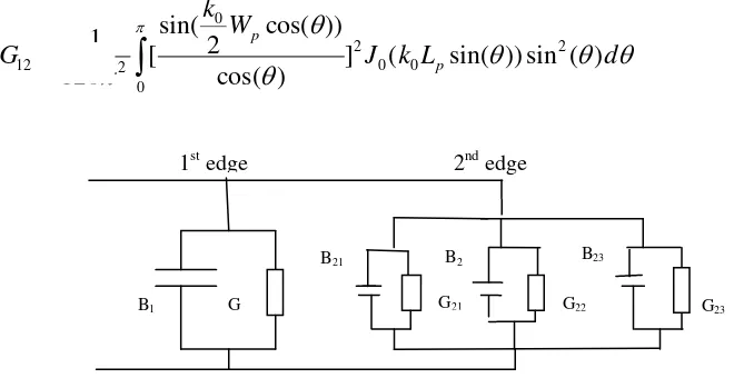
r = c/fr) .Fig. 1 illustrates that each radiating edge of the patch is represented by the admittance (Y) of real part denoted by conductance (G) and the imaginary part denoted by susceptance (B), so that Y = G + jB. To enhance the conventional rectangular UWB antenna, we divided the upper patch edge into three sub-edges (fingers) by making two slots of equal dimensions through the upper patch edge. These three fingers were proposed to increase the radiation area and to get three resonant frequencies that used to expand the bandwidth. For resonant input resistance analysis, the admittances of the fingers are Y21, Y22, and Y23, where Y21 = G21 + jB21, Y22 = G22 + jB22, and Y23 = G23 + jB23. Y2 is the parallel equivalent admittance of Y21, Y22, and Y23, and it is equal to G2 + jB2. Since the fingers are identical, G2 = G21 = G22 = G23, and B2 = B21 = B22 = B23, therefore G1 = G2 and B2 = -B1. As the total resonant input admittance is real, the total input resistance also is real, and it is given by [22]:
1 2 1
(
21 22 23)
13
24
1in
1
1
1
4
inin
R
Y
G
(7)
When the mutual effects are taken into account to calculate the exact value of the input impedance, mutual conductance exists between the edges of the patch, so the input resistance can be expressed as:
1 12
1
(
0)
(
)
4(
)
in s
R L
G
G
(8)
where G1 is the conductance of the bottom edge of the patch and G12 is the mutual conductance between upper and lower edges of the patch. The signs (+) and (-) are used for modes by odd and even resonant voltage distribution, respectively.
2
(
)
(
0) cos (
)
in s in s s
p
R
L
value
R
L
L
L
(9)
where Rin (Ls = value) is the input impedance at Ls inset feed point and can be taken as 50 Ω. Rin(Ls = 0) is the input impedance at the top edge of the patch, and, when Wp <
:1
1
(
)
90
pW
G
(10)
The mutual conductance (G12) can be determined by equation (11), where J0 is the Bessel function of the current density at zero order. By equations (9-11), the depth of each slot (Ls) was calculated to be 10 mm through the antenna patch [20].
0
2 2
12 2 0 0
0
sin(
cos( ))
1
2
[
]
(
sin( )) sin ( )
120
cos( )
p
p
k
W
G
J k L
d
(11)
Figure 1. Equivalent circuit of the transmission model
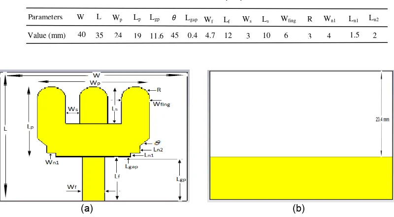
The schematic simulated diagram was derived from the reference rectangular antenna with rectangular printed patch on the front side of the Taconic TLY-5 substrate of thickness 1.575 mm and dielectric constant of 2.2. This geometrical diagram of front and back view is shown in Fig. 2 with all dimensions are defined in Table 1. In this design, there four parameters: feeder width, feed gap space, number of cut slots, and number of cut notches were modified to achieve a wider impedance bandwidth and a better impedance matching.
G23 1st edge 2nd edge
G
B1 G21
B21 B2
G22
Table 1. Dimensions of the proposed antenna
(a) (b)
Figure 2. Dimensions of the proposed antenna (a) front view, (b) back view
3. Geometry of the Fabricated and Printed Antenna
The overall structure of the antenna was successfully fabricated using Taconic TLY-5 material for substrate and copper of 0.035 mm thickness to print radiator and ground plane to be integrated with other system elements. The geometry of the fabricated design is shown in Fig. 3 of prototype mounted on the mentioned material substrate with connector of 50 Ω input impedance.
(a) (b)
Figure 3. The fabricated antenna being tested on anechoic chamber and network analyzer: (a) front view; (b) back view
4. Simulated and Practical Results and Discussion for the Proposed Antenna
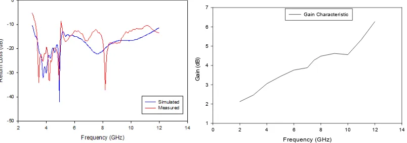
The performance of an antenna can be measured based on its reduction of the reflection power requirement on the transmission line to the source, which depends on the voltage reflection coefficient at the input terminals of the antenna. The practical and simulation frequency band was 3-12 GHz (ratio bandwidth was 4:1) for the designed antenna to determine its stable radiation characteristics. Fig. 4 illustrates the experimental and simulated return loss
Parameters Value (mm)
W L Wp Lp Lgp ߠ Lgap Wf Lf Ws Ls Wfing R Wn1 Ln1 Ln2
(|S11|dB) against the frequency band of the partially-grounded substrate antenna throughout the UWB frequency. The measured and simulated reflection coefficients (S11 < -10 dB) of the antenna are displayed, and they matched the broadband impedance characteristics. The |S11| less than -10 dB bandwidth that from the network analyzer test and the CST software was 3 to 12 GHz within little tolerance variations to give a good estimation of the performance of the antenna. These little losses in the fabrication tolerance and 50 Ω connector caused the variation between the simulated and measured characteristics of S11. From simulated S11, resonance frequencies of 4 GHz, 5 GHz, and 7.6GHz employ at -34 dB, -44dB, and -24dB respectively while in fabricated S11, resonance frequencies of 3.5 GHz, 4.5 GHz, 5 GHz, and 8.1 GHz employ at -35 dB, -33dB, -44dB, and -38dB respectively. Fig. 5 shows the gain characteristics of the proposed antenna versus frequency for the UWB bandwidth. The gain increased as frequency increased and the maximum value occurred at the end of the operating frequency band.
Frequency (GHz)
0 2 4 6 8 10 12 14
Ga
in
(
d
B
)
1 2 3 4 5 6 7
Gain Characteristic
Figure 4. Simulated and measured S11 of Figure 5. Characteristics of antenna gain with the proposed antenna increasing bandwidth for the proposed design
Frequency (GHz)
2 4 6 8 10 12 14 16
R
e
tu
rn
L
o
s
s
/
d
B
-40 -35 -30 -25 -20 -15 -10 -5 0
Simulated S11 at patch of two notches Simulated S11 at patch of one notch
Frequency (GHz)
2 4 6 8 10 12 14 16
R
e
tu
rn
L
o
s
s
/
d
B
-40 -35 -30 -25 -20 -15 -10 -5
Simulated S11 of patch with no slot Simulated S11 of patch with one slot Simulated S11 of patch with two slots
(a) (b)
Frequency (GHz)
2 4 6 8 10 12 14 16
R
e
tu
rn
L
o
s
s
/
d
B
-40 -35 -30 -25 -20 -15 -10 -5
Simulated S11 at feed width of 4.7 mm Simulated S11 at feed width of 4.5 mm Simulated S11 at feed width of 4.2 mm
Frequency (GHz)
2 4 6 8 10 12 14 16
R
e
tu
rn
Lo
s
s
/ d
B
-40 -35 -30 -25 -20 -15 -10 -5
Simulated S11 with 0.15 mm gap Simulated S11 with 0.25 mm gap Simulated S11 with 0.4 mm gap
(c) (d)
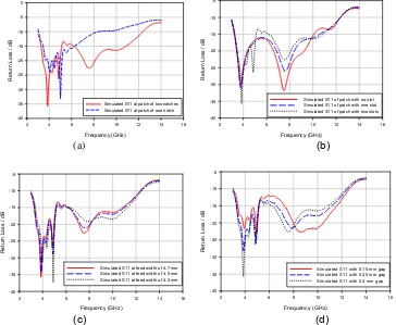
Figure 6. Proposed parametric study; (a) number of notch, (b) number of slot, (c) feeder width, (d) feed gap size
Fig. 7 shows the three-and two-dimensional, omni-directional patterns at frequency of 7.5 GHz, which describe antenna’s performance over the entire UWB bandwidth. Simulated current distributions are illustrated in Figure 8 at resonant frequencies of 5 and 3.8 GHz to facilitate the understanding of the antenna’s performance. For two set notches and two slots, the figure shows that the surface current on the radiator surface of the antenna was greater at resonant frequency of 5 GHz than that at 3.8 GHz. The peak values of the surface current distribution of the UWB radiator at the notches and the slotted edge was 63.7 A/m at 5 GHz and 23.1 A/m at 3.8 GHz; these values were greater than those presented in [19] at the steppers and convex corners of the radiator. From the simulation results, the values of the proposed antenna design parameters are presented in Table 2 antenna for the chose frequencies over the coverage UWB bandwidth.
Table 2. The values of antenna parameters at specified UWB frequencies
Parameters S11
4 GHz 6 GHz 8 GHz 10 GHz
Gain Directivity
Radiation efficiency Max power pattern
4.516dB -32 dB
3.062 dB 2.194 92.26 % 0.1608 VA/m2
-18 dB -23 dB -17 dB 2.736 dB 4.529 dB
(a) (b)
Figure 7. Simulated radiations at 7.5 GHz: (a) three-dimensional radiation pattern; (b) two-dimensional radiation pattern
(a) (b)
Figure 8. Simulated distribution of current on the surface of the proposed antenna at (a) 5 GHz and (b) 3.8 GHz
-30-25-20 -15-10 -5 0 -30 -25 -20 -15 -10 -5 0 -30 -25 -20 -15 -10 -5 0 -30 -25 -20 -15 -10 -5 0 0 30 60 90 120 150 180 210 240 270 300 330 Simulated E-plane at Phi=0 Simulated E-plane at Phi=90
-30-25-20-15-10 -5 0 -30 -25 -20 -15 -10 -5 0 -30 -25 -20 -15 -10 -5 0 -30 -25 -20 -15 -10 -5 0 0 30 60 90 120 150 180 210 240 270 300 330 Simulated E-plane at Phi=0 Simulated E-plane at Phi=90
-30 -25-20 -15-10 -5 0 -30 -25 -20 -15 -10 -5 0 -30 -25 -20 -15 -10 -5 0 -30 -25 -20 -15 -10 -5 0 0 30 60 90 120 150 180 210 240 270 300 330 Simulated E-plane at Phi=0 Simulated E-plane at Phi=90
E-plane E-plane E-plane
-30 -25 -20-15 -10 -5 0 -30 -25 -20 -15 -10 -5 0 -30 -25 -20 -15 -10 -5 0 -30 -25 -20 -15 -10 -5 0 0 30 60 90 120 150 180 210 240 270 300 330 Simulated H-plane at Theta=0 Simulated H-plane at Theta=90
-30 -25 -20-15 -10 -5 0 -30 -25 -20 -15 -10 -5 0 -30 -25 -20 -15 -10 -5 0 -30 -25 -20 -15 -10 -5 0 0 30 60 90 120 150 180 210 240 270 300 330 Simulated H-plane at Theta=0 Simulated H-plane at Theta=90
-30-25-20-15-10 -5 0 -30 -25 -20 -15 -10 -5 0 -30 -25 -20 -15 -10 -5 0 -30 -25 -20 -15 -10 -5 0 0 30 60 90 120 150 180 210 240 270 300 330 Simulated H-plane at Theta=0 Simulated H-plane at Theta=90
H-plane H-plane H-plane (a) (b) (c)
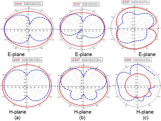
Fig. 9 shows the simulated radiation patterns of the far-field antenna at the x-y H-plane (Theta = 0o, 90o) and at the y-z E-plane (Phi = 0o, 90o). These patterns were compared with different values of frequency, i.e., 4.5, 7, and 10 GHz for the H-plane and the E-plane. The radiation patterns essentially were omni-directional in the E and H planes for the simulation of the proposed antenna.
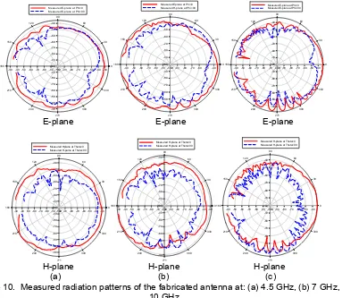
The fabricated antenna was tested using anechoic chamber by fixing the antenna on a stand using 50 Ω connector which is soldered at the lower edge of the feed line. So that by Anechoic chamber and network analyzer, the elevation (E-plane) and azimuth (H-plane) patterns were measured for the proposed antenna in a planes containing feed. These measured radiation patterns are shown in Fig. 10 at three operating frequencies: 4.5 GHz, 7 GHz, and 10 GHz in H-plane (xz-plane) and E-plane (xy-plane) and a little change in patterns due to frequency increase. The measured E-planes and H-planes show mostly omni-directional radiation patterns over the specified frequencies. In measured patterns, there are many ripples at the radiation amplitude due to into the field reflections from antenna holder, chamber scattering, and from inside of the anechoic chamber. To the proposed design with those of [4] and [7], the proposed finger-shaped antenna is smaller in dimension size, higher gain, using lighter and cheaper substrate material, and more stable omni-directional radiation patterns.
-100 -90-80-70-60-50-40-30 -100 -90 -80 -70 -60 -50 -40 -30 -100 -90 -80 -70 -60 -50 -40 -30 -100 -90 -80 -70 -60 -50 -40 -30 0 30 60 90 120 150 180 210 240 270 300 330 Measured E-plane at Phi=0 Measured E-plane at Phi=90
-100-90-80-70 -60-50-40 -100 -90 -80 -70 -60 -50 -40 -100 -90 -80 -70 -60 -50 -40 -100 -90 -80 -70 -60 -50 -40 0 30 60 90 120 150 180 210 240 270 300 330 Measured Eplane at Phi=0 Measured H-plane at Phi=90
-100 -90-80-70 -60-50 -40 -100 -90 -80 -70 -60 -50 -40 -100 -90 -80 -70 -60 -50 -40 -100 -90 -80 -70 -60 -50 -40 0 30 60 90 120 150 180 210 240 270 300 330 Measured E-plane at Phi=0 Measured E-plane at Phi=90
E-plane E-plane E-plane
-100 -90 -80 -70 -60 -50 -40 -30 -100 -90 -80 -70 -60 -50 -40 -30 -100 -90 -80 -70 -60 -50 -40 -30 -100 -90 -80 -70 -60 -50 -40 -30 0 30 60 90 120 150 180 210 240 270 300 330 Measured Hplane at Theta=0 Measured H-palne at Theta=90
-100 -90-80-70-60-50-40-30 -100 -90 -80 -70 -60 -50 -40 -30 -100 -90 -80 -70 -60 -50 -40 -30 -100 -90 -80 -70 -60 -50 -40 -30 0 30 60 90 120 150 180 210 240 270 300 330 Measured H-plane at Theta=0 Measured H-plane at Theta=90
-100 -90 -80 -70-60 -50 -40 -100 -90 -80 -70 -60 -50 -40 -100 -90 -80 -70 -60 -50 -40 -100 -90 -80 -70 -60 -50 -40 0 30 60 90 120 150 180 210 240 270 300 330 Measured H-plane at Theta=0 Measured H-plane at Theta=90
H-plane H-plane H-plane (a) (b) (c)
Figure 10. Measured radiation patterns of the fabricated antenna at: (a) 4.5 GHz, (b) 7 GHz, (c) 10 GHz
5. Conclusions
measured results for the most important antenna parameters such as return loss (S11<-10 dB) and omni-directional radiation patterns.
References
[1] Mohamed NS .Chapter 10 in Antenna Handbook of Ultra Wideband Communications: Novel Trends Antennas and Propagation. University Campus. Shanghai, China. 2011; 09.
[2] AF Molish, K Balakrishnan, D Cassioli, CC Chong, S Emami, J Karedal. IEEE 802.15.4a Channel Model-Final report. Task group 4a (TG4a), Tech. Report, 2004.
[3] Zaini KD, Meriah SM. New Diamond Antenna for Ultra Wideband Applications. IJCSI International Journal of Computer Science Issues. 2012; 9(4).
[4] Yusnita R, Razali N, Tharek AR. Chapter 18 of Ultra Wideband Handbook. University Campus. Shanghai. China. 2010.
[5] Hans GS. Smart Antenna for Spatial Rake UWB Systems. IEEE conference on ultra wideband systems and technologies. 2004.
[6] Tajeswita G, PK Singhal. Ultra Wideband Slotted Microstrip Patch Antenna for Downlink and Uplink Satellite Application in C band. International Journal of Innovation and Applied Studies. 2013; 3(3): 680-684.
[7] A Karmarkar, S Verma, M Pal, R Ghatak. An Ultra Wideband Monopole Antenna with Multiple Fractal Slots with Dual Band Rejection Characteristics. Progress In Electromagnetics Research. 2012;31: 185-196.
[8] E Antonino-Daviu, M Gallo, M Cabedo-Fabres, M Ferrando-Bataller. Novel Ultra Wideband Antenna for Diversity Applications. IEEE Conference. Bari. Italy. 2010.
[9] AD Capobianco, FM Pigozzo, A Locatelli, D Modotto. Chapter 1 (Directive Ultra-Wideband Antennas) in Microwave and Millimeter Wave Technologies Modern UWB Antennas and Equipment Handbook. University Campus. Shanghai. China. 2010.
[10] B Kasi, CK Chakrabarty. Ultra-Wideband Antenna Array Design for Target Detection. Progress in Electromagnetics Research. 2012;25: 67-79.
[11] MY Alhefnawy, Aladdin A, Hosny A, A Safwat, MI Youssef. Design and Implementation of a Novel Planar UWB Monopole Antenna for Multipath Environments. 13th International Conference on Aerospace Sciences & Aviation Technology, Cairo, Egypt. 2009.
[12] H Oraizi, B Rezaei. Combline Loadings of Printed Triangular Monopole Antennas for the Realization of Multi-Band and Wideband Characteristics. Progress In Electromagnetic Research B. 2012; 39: 179-195.
[13] Mishra SK, Gupta RK, Vaidya A, Mukherjee J. Printed Fork Shaped Dual Band Monopole Antenna for Bluetooth and UWB Applications With 5.5GHz WLAND Band Notched Characteristics. Progress In Electromagnetics Research C. 2011; 22: 195-210.
[14] DO Kim, NI Jo, HA Jang, CY Kim. Design of the Ultra Wideband Antenna with a Quadruple-Band Rejection Characteristics Using a Combination of the Complementary Split Ring Resonators.
Progress In Electromagnetics Research. 2011; 112: 93-107.
[15] P Tilanthe, PC Sharma, TK Bandopadhyay. A Monopole Microstrip Antenna with Enhanced Dual Band Rejection for UWB Applications. Progress In Electromagnetics Research. 2012; 38: 315-331. [16] Y Zhuo, L Yan, X Zhao, K Huang. A Compact Dual-Band Patch Antenna for WLAN Applications.
Progress In Electromagnetics Research Letters. 2011; 26: 153-160.
[17] Jia L, Shu L, Yu T, Liwen J, Mengqian L, Zhihua Z. The Simulation and Experiment of a UWB Printed Dipole Antenna. Progress In Electromagnetics Research Letters. 2013; 36: 21-30.
[18] Mai AR, Osman M, KA Rahim, M Azfar, NA Samsuri, F Zubir, K Kamardin. Design Implementation and Performance of Ultra-Wideband Textile Antenna. Progress In Electromagnetics Research B.
2011;27: 307-325.
[19] AHM Zahirul A, Rafiqul I, Sheroz K. Design of a Tuning Fork type UWB Patch Antenna. Int. Journal of Electrical and Electronics Engineering. 2006: 1-8.
[20] CA Balanis. Antenna Theory: Analysis and Design. By John Wiley & Sons. INC. 2013.
[21] KK Parashar. Design and Analysis of I-Slotted Rectangular Microstrip Patch Antenna for Wireless Application. International Journal of Electrical and Computer Engineering (IJECE). 2014; 4(1): 31-36. [22] WF Richards. Microstrip Antennas, Chapter 10 in Antenna Handbook: Theory, Applications and
Design. Van Nostrand Reinhold Co. New York. 1988.