UNIVERSITI TEKNIKAL MALAYSIA MELAKA
PSM TITLE:
DESIGN AND DEVELOPMENT OF WIRELESS POWER
TRANSFER FOR IMPLANT BIOMEDICAL DEVICE (PTIBD)
This report is submitted in accordance with the requirement of Universiti Teknikal Malaysia Melaka (UTeM) for the Bachelor of Electronic Engineering Technology
(Industrial Electronic) with Honours
by
NOR SYAIRAH BINTI SALLEH B071210097
890303085492
Disahkan oleh:
TANDATANGAN PENULIS TANDATANGAN PENYELIA
Cop Rasmi:
Alamat Tetap:
Blok D38, Fasa 3A Seri Manjung,
32040 Bandar Baru Seri Manjung,
Perak Darul Ridzuan
Tarikh: 12 January 2016 Tarikh: 12 January 2016
UNIVERSITI TEKNIKAL MALAYSIA
MELAKA
BORANG PENGESAHAN STATUS LAPORAN PROJEK SARJANA MUDA
TAJUK: Design and Development of Power Transfer for Implant Biomedical Device
(PTIBD)
SESI PENGAJIAN: 2014/ 2015 Semester 2
Saya NORSYAIRAH BINTI SALLEH
mengaku membenarkan Laporan PSM ini disimpan di Universiti Teknikal Malaysia Melaka (UTeM) dengan syarat syarat kegunaan seperti berikut:
1. Laporan PSM adalah hak milik Universiti Teknikal Malaysia Melaka dan penulis. 2. Perpustakaan Universiti Teknikal Malaysia Melaka dibenarkan membuat salinan
untuk tujuan pengajian sahaja dengan izin penulis
3. Perpustakaan dibenarkan membuat salinan laporan PSM ini sebagai bahan pertukaran antara institusi pengajian tinggi.
4. **Sila tandakan( ) sebagaimana yang termaktub dalam AKTA RAHSIA RASMI 1972)
(Mengandungi maklumat TERHAD yang
telahditentukan oleh organisasi/ badan dimana penyelidikan dijalankan)
**Jika laporan PSM ini SULIT atau TERHAD, sila lampirkan surat daripada pihak berkuasa/ organisasi
berkenaan dengan menyatakan sekali sebab tempoh laporan PSM ini perlu dikelaskan sebagai SULIT
i
DECLARATION
I hereby, declared this report entitled “Design and Development of Power Transfer for Implant Biomedical Device (PTIBD)” is results of my own research except as cited in references.
Signature :
ii
APPROVAL
This report is submitted to the Faculty of Engineering Technology of UTeM as a partial fulfilment of the requirements for the Universiti Teknikal Malaysia Melaka (UTeM) the Bachelor of Electronic Engineering Technology (Industry) with Honours (JTKEK). The member of supervisory is as follow:
:
iii
ABSTRAK
iv
ABSTRACT
v
DEDICATION
vi
ACKNOWLEDGEMENT
vii
LIST OF ABBREVIATIONS, SYMBOLS AND NOMENCLATURE ... xiv
CHAPTER 1... 1
2.1 Introduction of Literature Review ... 4
viii
2.7 Voltage regulator ...20
2.7.1 DC Voltage Stabilizers ...21
2.7.2 Active Regulators ...21
2.8 Rectifier ...22
2.8.1 Half-wave Rectification ...23
2.8.2 Full-wave Rectification ...24
2.8.3 Peak Loss ...25
2.8.4 Rectifier Output Smoothing ...25
2.9 Based on Journal ...27
2.9.1 Introduction and Basic Magnetic ...27
2.9.2 Magnetic Field Relationships ...28
CHAPTER 3...29
METHODOLOGY...29
3.1 Introduction of Methodology ...29
3.2 Overall Process Flow ...29
3.3 Block Diagram the Description of this Project ...31
3.4 Generate Conceptual Design of PSIBD Structure...32
3.5 Define Component Used in Circuit ...33
ix
3.6.4.1 Sausage ...54
3.6.5 Transformer ...55
CHAPTER 4...56
RESULT & DISCUSSION ...56
4.1 Introduction of Result and Discussion...56
4.2 Analysis at Software Circuit ...56
4.2.1 Result 1: Analysis the Output Voltage...57
4.2.2 Result 2: Analysis Output Waveform ...59
4.3 Analysis at Hardware Circuit on Tektronix Oscilloscope ...61
4.3.1 Result 1: Analysis Output Voltage at Timer 555 ...61
4.3.2 Result 2: Analysis the Highest Voltage when Changing Frequency ..63
4.4 Result 3: Determine the voltage transfer without skin and skin ...64
4.4.1 Without skin (no sausage) ...65
4.4.2 With skin (with sausage) ...68
CHAPTER 5...72
CONCLUSION AND FUTURE WORK ...72
5.0 Introduction ...72
5.1 Summary of Project ...72
5.2 Summary of Research ...73
5.3 Achievement of Research Objectives ...73
5.4 Problem Arising ...73
5.5 Suggestion for the Future Work ...74
REFERENCES ...75
APPENDICES ...77
x
LIST OF TABLES
Table 2. 1: Different Wireless Power Technologies Uses ... 8
Table 2.2: The Frequencies on Each Different Value of Capacitor and Resistor ...19
Table 2.3: Type of LM78xx Voltage Regulators ...20
Table 3.1: Comparison FET and BJT ...40
Table 3.2: Complementary NPN and PNP Transistor’s ...40
Table 4.1: Data Output Voltage from Oscilloscope Multisim: ...58
Table 4.2: Output Waveform when Supply Difference Voltage ...61
Table 4.3: Voltage Output Versus Frequency ...63
Table 4.4: Data from Oscilloscope for Circuit without Skin ...67
xi
LIST OF FIGURES
Figure 2.1: Block Diagram of a Wireless Power System... 9
Figure 2.2: Block Diagrams of an Inductive Wireless Power System... 9
Figure 2.3: Concept Wireless Transfer to Charging Phone ...10
Figure 2.4: Boost Inductor Simple Circuit and Boost Transformer Simple Schematic ...12
Figure 2.5: Simple Circuit Combining Forward Converter and Flyback ...13
Figure 2.6: Push-Pull Center Tap, Simple Forward (Buck) Converter Schematic...13
Figure 2.7: Push- pull Boost, Simple Circuit Schematic ...13
Figure 2.8: Example of Wave’s Oscillator ...14
Figure 2.9: Type of Timer 555 ...15
Figure 2.10: Actual Pin Number and the Function ...16
Figure 2.11: Actual Pin Timer 555 Arrangement ...16
Figure 2.12: An Astable Circuit for Timer 555 ...17
Figure 2.13: Timer 555 Output Square Wave ...18
Figure 2.14: Example of Circuit Half-wave Rectifier ...23
Figure 2.15: Gratzbridge Rectifier (Full-Wave Rectifier Using 4 diodes) ...24
Figure 2.16: Full-Wave Rectifier (using a Transformer and 2 diodes) ...24
Figure 2.17: 3-Phase AC Input, Half & Full Wave Rectified and DC Output Waveforms ...25
Figure 2.18: RC-Filter Rectifier ...26
Figure 2.19: Circuit of Magnetic Field ...27
Figure 2.20: Field Around Conductor ...28
Figure 2.21: Sinusoidal Voltage Drive ...28
Figure 3.1: Flow Chart Overall Project ...30
Figure 3.2: Block diagram for External Circuit...31
Figure 3.3 Block Diagram for Internal Circuit 31
Figure 3.4: Expected Circuit for PTIBD ...32
Figure 3.5: Polarization of the Duty Cycle ...36
Figure 3.6: Output Square Wave and Capacitor Charging Signal ...36
xii
Figure 3.8: Visual of Transistor 2N3904 and 2N3907 ...38
Figure 3.9: Configuration of NPN 2N3904 and PNP 2N3906 ...38
Figure 3.10: Operation of PNP and NPN of Transistor ...39
Figure 3.11: Diode ...41
Figure 3.12: Wave of Rectifier ...41
Figure 3.13: LM7805 Voltage Regulator ...42
Figure 3.14: Fixed Output Voltage ...43
Figure 3.15: Position of Coil ...44
Figure 3.16: Flow of Magnetic Field ...46
Figure 3.17: Overall Circuit for PTIBD ...47
Figure 3.18: Isis External Circuit ...48
Figure 3.19: Internal Circuit ...49
Figure 3.20:PCB layout for External Circuit...49
Figure 3.21: 3D Visualization for External Circuit ...50
Figure 3.22: PCB Layout for Internal Circuit ...50
Figure 3.23: 3D Visualization for Internal Circuit ...51
Figure 3.24: Etching Process ...52
Figure 3.25: Soldering Process ...52
Figure 3.26: PCB Board for External Circuit ...53
Figure 3.27: PCB Board for Internal Circuit ...53
Figure 3.28: Completed PCB Circuit 54
Figure 3.29: Sausage Replaced the Skin ...54
Figure 3.30: Ferrite E core ...55
Figure 3.31: Difference Size of Coil ...55
Figure 3.32: Winding Process ...55
Figure 4.1: Output Voltage from Multism Circuit...57
Figure 4.2: Output Voltage from CH1, CH2, CH3 and CH4 ...58
Figure 4.3: Output Voltage after Timer 555 ...59
Figure 4.4: Output Voltage at Primary Transformer ...60
Figure 4.5: Output Voltage at Secondary Transformer ...60
Figure 4.6: Primary Board Circuit ...61
xiii
Figure 4.8: Duty Cycle when Supply 10 V ...62
Figure 4.9: Voltage Output Versus Frequency ...63
Figure 4.10: Experiment on Circuit ...64
Figure 4.11: Experiment Without Skin ...65
Figure 4.12: Flow Chart Procedure for Experiment Without Skin...66
Figure 4.13: Output Without Skin at Primary Transformer ...67
Figure 4.14: Output Without Skin at Secondary Transformer ...67
Figure 4.15: Experiment with Skin ...68
Figure 4.16: Flow Chart Procedure for Experiment with Skin ...69
Figure 4.17: Output with Skin at Primary Transformer ...70
Figure 4.18: Output with Skin at Secondary Transformer ...70
xiv
LIST OF ABBREVIATIONS, SYMBOLS AND NOMENCLATURE
PSM - Project Sarjana Muda
PTIBD - Power Transfer Implant Biomedical Device BJT - Bipolar Junction Transistor
FET -Field Effect Transistor
Vs - Voltage Source
Vs - Secondary induces voltage of ideal transformer Vp - Primary induces voltage of ideal transformer Ns - Number of turn in the secondary coil
Vrms - the root-mean-square value of output voltage.
π - Pai
e - Exponent
1
CHAPTER 1
INTRODUCTION
1.1 Background
2
1.2 Problem Statement
Nowadays, many devices for implanted biomedical just have battery to maintain the power. The battery was functions only in below 10 years. Now, the project is created to help the devices always work even if the battery is dead. Besides that, implanted biomedical devices such as pacemaker must have power to generate electrical stimulation. It is not easy to transfer power because it resides inside the human body. Based on this problem, the project must be designed circuit to supply sufficient power to the battery of pacemaker inside the body. This project has two circuit had been created which is external and internal circuit. External part is a function to transmit power. Internal part is function to receive power from external and recharges the battery in implant device. Expected result for this project is transformer can transfer more power and has the ability to charge the implanted device.
1.3 Objective
This objective of this project is must be able:
1. To design a power transfer circuit between external and internal part. 2. To analysis the input and output voltage at external and internal circuit of
3
1.4 Scope
Scope of this project is to develop the charger battery for pacemaker. Firstly, circuit of charging battery must designed external and internal circuit. External circuit comes from outside the body and internal comes inside the body. Circuit from external side can transfer power to pacemaker device. From internal side it can get the power to recharging battery to pacemaker. This is called wireless power transfer. Next, the data must collected based on analysis the input and output voltage at external and internal circuit of PTIBD
1.5 Structure/Summary of this Report
4
CHAPTER 2
LITERATURE REVIEW
2.1 Introduction of Literature Review
This chapter was researches about theory related to the project based on journal, book or other references. Begun, to characterize the hardware and related law sample wireless power transfers.
2.2 History about Battery in Pacemaker
Has reported in worldwide about that 600,000 pacemakers are embedded and the aggregate number of individuals utilized with various sorts of introduced pacemaker has been crossed 3 million clients. Pacemaker is used half of its battery power for cardiovascular pacemaker instigation and the other half for routine exercises. The crucial history about batteries in cardiovascular pacemakers is utilized nickel-cadmium rechargeable battery. Next zinc-mercury battery was made and just life is which proceeded for more than 2 years. At 1972, Wilson creates the best batteries because survived period for battery life was taking a long time. The pacemaker unit goes on an electrical heartbeat with the best energy to the best area to vitalize the heart at a favoured rate
5 force supply (battery) and solidified substitute parts. The pacemaker unit is typically introduced in the pectoral zone (Sandro A. P. Haddad, 2009). In year 1958, a thoracic master at Karonlinska Hospital in Stockholm do embedded myocardial terminals and heartbeat generator with a rechargeable nickel-cadmium on 40 year old patient but the beat generator is fizzled inside of a few hours and function back on around 6 weeks.
In 1960, ten patients had profitable implantation because that year was introduce pacemakers which been developed. The batteries in pacemakers are basic in basic bit of the beat at terms of weight, volume and size. Immovable quality is fundamental segment for a heart pacemaker battery and for information batteries in implantable gadgets can't be supplanted. A decent battery configuration is a trade off between different and execution parameters to meet the prerequisites of the particular application
6 Still some rechargeable pacemakers being used however not sold any more and that not have individual to redesign the method for improvement. The rechargeable battery simply made on nickel-cadmium but it not gives benefit. All things need take considered, voltages of battery pacemaker range in 2.5 V until 10 V. Around 1960s mercury-zinc batteries is given 4-8 V. Since 1970s, lithium batteries are suitable and helpful for pacemaker. In that lithium has the most critical element. The begun of lithium iodine battery in 1975 for supplanted the mercury-zinc battery is altogether enlarged the pacemaker battery life for more than 10 years for a couple models. The factor of lithium is reacts violently with water and an extensive variety of materials such as sulfur di-thionyl chloride, manganese dioxide besides carbon monofluoride is used for the dynamic cathode material. Then, Lithium has long life, little exhaust current and voltage traits
2.3 Wireless Power Transfer
Transmission of electrical power from fundamental power to devouring without utilizing strong wires or conductor is called the Wireless power transfer. (Yakovlev, Kim, & Poon, 2012). This is term that implies various diverse power transmission innovations that uses in time varying electromagnetic fields. Wireless transmission only used for power electrical devices when has interconnecting wires has been troublesome, dangerous or doubtful. On wireless power transfer has transmitter device which associated with power source. It means the main power line can transmits power by electromagnetic fields across at intervening space. Receiver devices has been converted back to electric power and utilized.
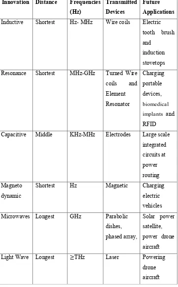
8 Table 2.1: Different Wireless Power Technologies Uses
Innovation Distance Frequencies (Hz)
Transmitted Devices
Future Applications
Inductive Shortest Hz- MHz Wire coils Electric tooth brush and
induction stovetops Resonance Shortest MHz-GHz Turned Wire
coils and
Capacitive Middle KHz-MHz Electrodes Large scale integrated
Shortest Hz Magnetic Charging
electric vehicles
Microwaves Longest GHz Parabolic