DOI: 10.12928/telkomnika.v13.i1.1122 364
Overview of Custom Microcontroller using Xilinx
Zynq XC7Z020 FPGA
Bayu Kanigoro* , Ricky Efraim Lie , and M. Fitra Kacamarga Computer Science Program, School of Computer Science, Bina Nusantara University
Jakarta, 11480, Indonesia
*Corresponding author, e-mail: [email protected]
Abstract
This paper presents an overview of customizable microcontroller using a Xilinx Zynq XC7Z020 FPGA as an alternative to increase its performance as user need. This alternative arises due to many of the systems, which developed mostly by using microcontroller are not giving any room for customization to increase its performance or I/O ports. There is any possibility that the system designed to be used by using general processor such as PC to increase its performance but it will give another problem such as interface difficulty for high speed I/O, real time processing, increases complexity, and many more. Customization is introduced by combining hard IP processor and FPGA in one chip instead of practicing two separate devices, processor and FPGA, which is commonly use in high performance embedded design. This approach allows seamless design development and development time reduction for customization.
Keywords: FPGA, microcontroller, embedded system, system-on-chip, customization
1. Introduction
The advancement of semiconductor technology has been reaching in nanometer scale which shown by Intel that has achieved 22nm process technology in 2011 for their processor products line [1]. This advancement has been giving an opportunity to put many functions on a chip beside main function such as a processor and their peripherals can be placed on a single chip. This development is rising some technics and methodologies for designing a silicon chip into a full functionality integrated circuit. One of the methods is Full Custom Design. In this method, an engineer designs some or all of the logic cells, circuits, or layout specifically for one design [2]. The other development of this advancement is possibility of customizing logic circuit on semiconductor without following expensive semiconductor fabrication processing technology due to all primitive gates have been implemented on it then users or developers only need to route interconnection between gates to create digital circuit and system. This technology is known as Field Programmable Gate Array or FPGA.
Giving that ability of FPGA technology creates a concept of soft processor. Soft proces-sor is a procesproces-sor, implemented in FPGA, which can be customized to meet application needs [3]. Xilinx and Altera have been developing MicroBlaze and NIOS II respectfully for their soft processor. MicroBlaze [4] is RISC Pipelined Big-Endian 32-bit processor developed by Xilinx in 2002. It has 32 32-bit general purpose registers and special registers such as Program Counter register. Microblaze has three and five pipeline stages which can be configured in development stage depending on area optimization which requires bigger area when using five stages pipeline. The limitations of soft processor compared to hard processor, which is implemented per-manently on the chip, are on area size, performance, and power consumption but soft processor has advantage by customization such as flexibility and special instruction for special application [3]. Soft processor has been used for many application. For example, worm robot [5], automotive application [6], increasing chipering algorithm performance [7], increasing application execution by moving part of the application usually executed by microprocessor into FPGA [8], increas-ing floatincreas-ing point performance in soft processor [9], FPGA based Programmable Logic Controller (PLC) [10, 11], and many more.
Recently in late 2011, Xilinx developed ZynqR–7000 All Programmable SoCs [13]. This
is the answer from Xilinx to include two application grade ARMR processors and FPGA on single
chip thus increasing computing performance than soft processor and, from designer perspective, maximizing precious FPGA resources only for custom design. The drawback of this approach is the architecture of the processor is permanently etched on chip hence giving no possibilities to customize its architecture as opposite of soft processor approach. This method will be called as System-on-Chip (SoC) approach in this paper as per definition all aspects of a digital system: processing, high-speed logic, interfacing, memory, and so on can be combined on same chip [14]. The purpose of this paper is giving a demonstration to develop custom microcontroller by using System-on-Chip (SoC) approach. As it is known that the architecture of a microcontroller in the market such as PIC Microchip [15, 16, 17], Intel MCS–51 [18, 19], and Atmel AVR Microcon-troller [20, 21, 22] are permanently etched on a silicon. Consequently closing any possibilities to alter or enhance their structure. Those microcontrollers have an advantage in price point of view due to very low price which is around 36 cent US dollars and satisfy for less complex requirement [23]. When the requirements and need of flexibility of the systems are raising, such as video processing [24, 25], then those microcontrollers, due to their limitations, are not capable to tackle the demands [26].
2. The Architecture
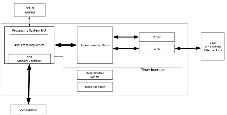
In general the architecture of System-on-Chip or SoC is combination of Processing Sys-tem, in this case ARM based processor, and programmable logic depicted in figure 1. The pro-cessing system has some interfaces to interact with outside environment which are Propro-cessing System I/O and DDR Memory Controller. Processing System I/O consists on several common interfaces that usually appears on small computer such as laptop or tablet PC. On Zynq plat-form, it has two USB ports, two Ethernet controller, SD controller, General Purpose I/O, and serial interface. Its DDR memory controller supports DDR3, DDR3L, DDR2, and LPDDR2 on Zynq platform hence Processing System can directly communicate to memory. There are interfaces to communicate between Processing System and Programmable Logic, which named Processor-Programmable Logic Interfaces showed in figure 1. For this, Xilinx uses AXI Interconnect for the interfaces [27].
Processor – Programmable Logic Interfaces
Figure 2 shows the architecture of the demonstration system. It consist of four main blocks and two supporting blocks. The main blocks are ARM Processing System with DDR Mem-ory Controller, Interconnection block, Timer and General Purpose Input Output (GPIO). The sup-porting blocks are Reset Control System and Clock Multiplier. ARM Processing System with DDR Memory Controller is hard implemented on the chip consequently their logic are permanent. Therefore, this blocks is placed and named as Processing System. The rest of blocks is placed on programmable logic.
ARM Processing System Interconnection Block
Reset Control System
Timer
GPIO
DDR3 SDRAM DDR Memory Controller
Clock Multiplier
LEDs DIP SWITCHs External Ports
Processing System I/O Serial Terminal
Timer Interrupt
Figure 2.System architecture of custom microcontroller
master-slave approach for them hence the processor becomes the master and the rest of devices, timer and GPIO, become slave.
The design employs two devices which are timer device with interrupt and General Pur-pose Input Output (GPIO). Timer is intended to demonstrate how processor in Processing System responds with interrupt request from timer device and GPIO becomes an interface from the sys-tem to external port which is connected to LEDs and switches. The other devices are serial terminal which is connected to Processing System I/O and DDR3 SDRAM which is connected to DDR Memory Controller. This two devices, Processing System I/O and DDR Memory Controller, are not implemented in Programmable Logic which is in FPGA but instead is implemented directly on the chip.
Two supporting devices in the design are clock multiplier and reset control system. Clock multiplier is required to supply processor and all the devices including memory with required clock signal from relatively low frequency input from clock generator. This usually can be implemented by using Phase Locked Loop [28]. The other role of clock multiplier is supplying clock for DDR SDRAM that requires90◦lead from main clock. Reset control system is required to synchronise reset all devices in the system from uncertainty states to initial state. Listing 1 shows port map of top level design of the system in VHDL.
begin
system_1_i : system_1 port map (
LEDs_8Bits_TRI_IO => LEDs_8Bits_TRI_IO ,
processing_system7_0_MIO => processing_system7_0_MIO , processing_system7_0_PS_CLK => processing_system7_0_PS_CLK , processing_system7_0_DDR_Clk => processing_system7_0_DDR_Clk , processing_system7_0_DDR_Clk_n => processing_system7_0_DDR_Clk_n , processing_system7_0_DDR_CKE => processing_system7_0_DDR_CKE , processing_system7_0_DDR_CS_n => processing_system7_0_DDR_CS_n , processing_system7_0_DDR_RAS_n => processing_system7_0_DDR_RAS_n , processing_system7_0_DDR_CAS_n => processing_system7_0_DDR_CAS_n , processing_system7_0_DDR_WEB_pin => processing_system7_0_DDR_WEB_pin , processing_system7_0_DDR_BankAddr => processing_system7_0_DDR_BankAddr , processing_system7_0_DDR_Addr => processing_system7_0_DDR_Addr ,
processing_system7_0_DDR_VRN => processing_system7_0_DDR_VRN , processing_system7_0_DDR_VRP => processing_system7_0_DDR_VRP ) ;
end a r c h i t e c t u r e STRUCTURE;
Listing 1.Top level port map of the system
3. Software Model
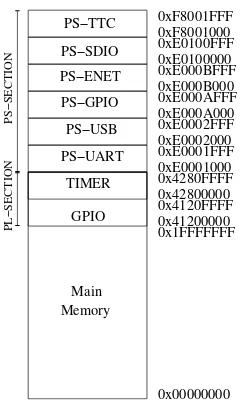
The software of this system is directly coded to the processor. This means, it does not need any operating system for running an application which is using the system. To access the devices or peripherals, it uses memory mapped I/O. Hence, the application can directly control it by accessing the address for the corresponding devices and sending the necessary values to it. This has some drawbacks that only one process can be executed by the processor at a time. By using memory mapped I/O for accessing the devices then the address of the devices is consecutive to memory address which shown in figure 3.
Giving an memory mapped I/O of the system in figure 3 shows a division of main memory and its corresponding devices. Main memory starts from address 0x00000000 to 0x1FFFFFF which gets 512 MB. This is where application software will be stored and executed by the system. Consequently, reset vector of the processor must be addressed to low address of the main mem-ory which is 0x00000000. The other devices, GPIO, is addressed at 0x41200000 to 0x4120FFFF which gets 64KB and Timer is addressed at 0x42800000 to 0x4280FFFF, which gets same as GPIO, 64KB. The memory is divided by two sections, PS-Section and PL-Section. PS-Section is part of Processing System then all devices in the PS-Section is fixed then it can not changed its structure. The other section is PL-Section which is part of Programmable Logic.
PS−SECTION
Figure 3.Memory Map of the system.
Accessing the GPIO can be fulfilled by using function that directly instruct it through mem-ory. For example, to write AXI GPIO made for Xilinx, the instruction [29, 30] is,
XGpio_DiscreteWrite(*gpioAddress, channel, state);
and to read AXI GPIO is,
XGpio_DiscreteWrite(*gpioAddress, channel);
The other device, Timer, is treated as same as GPIO which is directly configured by using direct memory instruction. In this system, Timer is using interrupt to notice the processor that counting process in the Timer has been ended. When the interrupt is asserted then program counter in the processor moves to special region in memory which named is interrupt or excep-tion region. The region will be filled with funcexcep-tions to respond what behaviour of the processor to expect. After the functions are finished executed then program counter will move to original location where main program is placed. Such example is from Xilinx, which uses AXI Timer [31] as implementation of this device. AXI timer uses four functions to control it [30]. First function to control the device is,
void XTmrCtr_Start(XTmrCtr *InstancePtr, u8 TmrCtrNumber)
This function is required to start the specified timer counter of the device such that it starts running. The timer counter is reset before it is started and the reset value is loaded into the timer counter [30]. The parameters of the function are InstancePtr which point to XTmrCtr instance to be worked on andTmrCtrNumberis the timer counter in the system to be worked on [30]. Second function to control it is,
void XTmrCtr_Stop(XTmrCtr *InstancePtr, Xuint8 TmrCtrNumber)
This function is required to stop the Timer from counting. The parameters of the function are
InstancePtr which point to XTmrCtr instance and TmrCtrNumber is the timer counter in the system to be worked on [30]. Third function is,
void XTmrCtr_Reset( XTmrCtr *InstancePtr, Xuint8 TmrCtrNumber)
which required to reset the Timer. And the last required function is,
void XTmrCtr_SetResetValue( XTmrCtr *InstancePtr, Xuint8 TmrCtrNumber, Xuint32 ResetValue )
This function is to set the reset value for the specified timer counter. The value is loaded into the timer counter when it is reset and also loaded when the timer counter is started. The parameters of the function areInstancePtrwhich point to XTmrCtr instance, andTmrCtrNumberis the timer counter of the device to operate on, andResetValuecontains the value to be used to reset the timer counter [30]. The value can be achieved by using this equation,
ttmr=
1
fclk× i<32
X
i=0
(n×2i) (1)
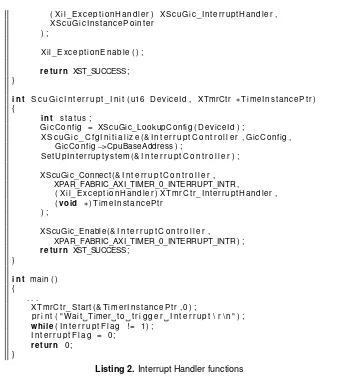
When the Timer uses interrupt then several functions is required to service the request from it. Listing 2 depicts the functions to handle interrupt request from Timer device.
void T i m e r _ I n t e r r u p t H a n d l e r (void ∗data , u8 TmrCtrNumber ) {
p r i n t ( " I n s i d e Timer ISR \ r \ n " ) ; XTmrCtr_Stop ( data , TmrCtrNumber ) ; XTmrCtr_Reset ( data , TmrCtrNumber ) ; p r i n t ( " Outside Timer ISR \ r \ n " ) ; p r i n t ( " \ r \ n " ) ;
I n t e r r u p t F l a g = 1 ; }
i n t S e t U p I n t e r r u p t S y s t e m ( XScuGic ∗X S c u G i c I n s t a n c e P o i n t e r ) {
( X i l _ E x c e p t i o n H a n d l e r ) X S c u G i c _ I n t e r r u p t H a n d l e r , X S c u G i c I n s t a n c e P o i n t e r
) ;
X i l _ E x c e p t i o n E n a b l e ( ) ;
r e t u r n XST_SUCCESS ; }
i n t S c u G i c I n t e r r u p t _ I n i t ( u16 DeviceId , XTmrCtr ∗T i m e I n s t a n c e P t r ) {
i n t s t a t u s ;
G i c C o n f i g = XScuGic_LookupConfig ( D e v i c e I d ) ;
X S c u G i c _ C f g I n i t i a l i z e (& I n t e r r u p t C o n t r o l l e r , GicConfig , GicConfig−>CpuBaseAddress ) ;
S e t U p I n t e r r u p t y s t e m (& I n t e r r u p t C o n t r o l l e r ) ;
XScuGic_Connect (& I n t e r r u p t C o n t r o l l e r , XPAR_FABRIC_AXI_TIMER_0_INTERRUPT_INTR ,
( X i l _ E x c e p t i o n H a n d l e r ) X T m r C t r _ I n t e r r u p t H a n d l e r , (void ∗) T i m e I n s t a n c e P t r
) ;
XScuGic_Enable (& I n t e r r u p t C o n t r o l l e r , XPAR_FABRIC_AXI_TIMER_0_INTERRUPT_INTR ) ; r e t u r n XST_SUCCESS ;
}
i n t main ( ) {
. . .
X T m r C t r _ S t a r t (& T i m e r I n s t a n c e P t r , 0 ) ;
p r i n t ( " Wait Timer t o t r i g g e r I n t e r r u p t \ r \ n " ) ; while( I n t e r r u p t F l a g ! = 1 ) ;
I n t e r r u p t F l a g = 0 ; r e t u r n 0 ;
}
Listing 2.Interrupt Handler functions
4. Result and Discussion
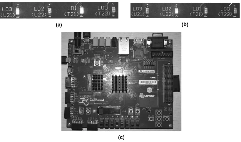
The system was implemented at Xilinx Zynq-7000 All Programmable SoC XC7Z020-CLG484-1 on ZedBoard development board [32] and Xilinx ISE 14.7 EDK as design tool. The development board is shown in figure 4c. Table 1 presents the utilization of register resource in XC7Z020-CLG484-1 gets around 0.13%, Look up Tables (LUT) which constitute logic resource of the FPGA get around 0.45%. Clock buffer gets around 3.125%, and I/O gets around 41.81%. The maximum frequency of this system is 216.973 MHz for -1 speed grade. This resources represents the architecture shown in figure 2 which implemented on programmable logic.
Table 1.Resource utilization of the system.
Resources Utilization
Registers 418 of 319200
LUT 728 of 159600
Clock Buffer 1 of 32
I/O 138 of 330
To demonstrate the system, the software was developed to show timer interrupt and GPIO capability. The action of the software was responding interrupt request when the timer has been reaching zero by turning on or off LEDs (LD0– LD7), which connected to GPIO, as shown in figure
(a) (b)
(c)
Figure 4. ZedBoard development board of the implemented system (figure 4c) and LEDs appearance of interrupt execution (figure 4a) and (figure 4b).
to show that the request has been executed which were initially0x04, which LD2was turned on
and the others were turned off (figure 4b) and0x0A, which LD3and LD1were turned on and the
rest were turned off showing that it has been executed successfully (figure 4a). The C statement that writes the GPIO into the value is,
XGpio_DiscreteWrite(&gpio,LED_CHANNEL, 0x04);
for initial status and this statement,
XGpio_DiscreteWrite(&gpio,LED_CHANNEL, 0x0A);
is executed when the request has been executed. The GPIO was initialized by using following statements shown in listing 3,
# define GPIO_LED_DEVICE_ID XPAR_LEDS_8BITS_DEVICE_ID # define LED_CHANNEL 1
XGpio g p i o ; . . .
i n t main ( ) {
. . .
x S t a t u s = X G p i o _ I n i t i a l i z e (& gpio , GPIO_LED_DEVICE_ID ) ; i f( x S t a t u s ! = XST_SUCCESS) {
p r i n t ( " GPIO I n i t F a i l e d \ n " ) ; r e t u r n 1 ;
} . . . }
Listing 3.GPIO initialization
has been reaching zero then execute the function by sending interrupt signal to processor and changes theInterruptFlagvariable to 1 followed by,
XGpio_DiscreteWrite(&gpio,LED_CHANNEL, 0x0A)
statement. The timer itself was configured by usingXTmrCtr_SetResetValuefunction followed by
0xf0000000as its parameter. The parameter took around 40.3 seconds for timer, which supplied by 100 MHz clock signal to reach zero.
Comparing the approach developed by Yang et.al [12] which combining two separate devices, ARM processor and FPGA, on a PCB, this approach gives less PCB footprint, simplified PCB design and gives better signal integrity.
5. Conclusion
FPGA combined by hard core processor gives a better customization for microcontroller to increase its performance. Hence, this model gives an alternative from conventional micro-controller. Sometimes, due to higher cost of FPGA comparing to conventional microcontroller, it becomes not so competitive hence a designer should weigh up which requirement needs for this model comparing to conventional microcontroller to get trade off between performance and product cost. For the system, it only use around one percent resource of XC7Z020-CLG484-1 to implement it, and the maximum frequency which can be used is 216.973 MHz.
Acknowledgement
This materiel is based on work supported by Bina Nusantara University under grant Hibah Bersaing Binus 015.A/VR.RTT/IV/2014 and Xilinx University Program.
References
[1] M. Bohr and K. Mistry, “Intel’s revolutionary 22 nm transistor technology,”Intel website, 2011. [2] M. J. Smith, “Application-specific integrated circuits,” 1997.
[3] P. Yiannacouras, J. G. Steffan, and J. Rose, “Application-specific customization of soft pro-cessor microarchitecture,” inProceedings of the 2006 ACM/SIGDA 14th international sym-posium on Field programmable gate arrays. ACM, 2006, pp. 201–210.
[4] Xilinx, “Microblaze processor reference guide v13. 4,”reference manual, 2011.
[5] J. González-Gómez, E. Aguayo, and E. Boemo, “Locomotion of a modular worm-like robot using a fpga-based embedded microblaze soft-processor,” inClimbing and Walking Robots. Springer, 2005, pp. 869–878.
[6] M. Hubner, K. Paulsson, and J. Becker, “Parallel and flexible multiprocessor system-on-chip for adaptive automotive applications based on xilinx microblaze soft-cores,” inParallel and Distributed Processing Symposium, 2005. Proceedings. 19th IEEE International. IEEE, 2005, pp. 149a–149a.
[7] I. Gonzalez and F. Gomez-Arribas, “Ciphering algorithms in microblaze-based embedded systems,” in Computers and Digital Techniques, IEE Proceedings-, vol. 153, no. 2. IET, 2006, pp. 87–92.
[8] R. Lysecky and F. Vahid, “Design and implementation of a microblaze-based warp processor,” ACM Trans. Embed. Comput. Syst., vol. 8, no. 3, pp. 22:1–22:22, Apr. 2009. [Online]. Available: http://doi.acm.org/10.1145/1509288.1509294
[9] J. Kadlec, R. Bartosinski, and M. Danek, “Accelerating microblaze floating point operations,” inField Programmable Logic and Applications, 2007. FPL 2007. International Conference on. IEEE, 2007, pp. 621–624.
[10] Q. Wei, Q. Cai, and C. Xie, “Research and implementation of plc editor system,” TELKOM-NIKA Indonesian Journal of Electrical Engineering, vol. 12, no. 3, pp. 2133–2137, 2014. [11] Z. Huabing, L. Benlei, D. Bolin, and F. Xiao, “Research on fpga-based programmable logic
[12] H. Yang, Y. Chen, and B. Chen, “An embedded auto-leveling system based on arm and fpga,” TELKOMNIKA Institute of Advanced Engineering and Science, vol. 11, no. 12, pp. 7094–7101, 2013.
[13] Xilinx. (2014, September) Zynq-7000 All Programmable SoC. [Online]. Available: http://www.xilinx.com/products/silicon-devices/soc/zynq-7000/
[14] L. H. Crockett, R. A. Elliot, M. A. Enderwitz, and R. W. Stewart, The Zynq Book, 1st ed. Strathclyde Academic Media, 2014.
[15] J. Iovine,PIC microcontroller project book. McGraw-Hill, Inc., 2004.
[16] D. Ibrahimet al.,Advanced PIC Microcontroller Projects in C: From USB to RTOS with the PIC 18F Series. Newnes, 2011.
[17] H.-W. Huang, PIC microcontroller: an introduction to software and hardware interfacing. CengageBrain. com, 2005.
[18] N. S. Kumar, M. Saravanan, and S. Jeevananthan, Microprocessors and Microcontrollers. Oxford University Press, Inc., 2011.
[19] S. Yeralan and A. Ahluwalia, Programming and interfacing the 8051 Microcontroller. Addison-Wesley Reading, 1995.
[20] D. V. Gadre,Programming and customizing the AVR microcontroller. McGraw-Hill, 2001, vol. 3.
[21] S. F. Barrett and D. J. Pack, “Atmel avr microcontroller primer: Programming and interfacing,”
Synthesis Lectures on Digital Circuits and Systems, vol. 2, no. 1, pp. 1–194, 2007.
[22] M. A. Mazidi, S. Naimi, and S. Naimi,Avr Microcontroller and Embedded Systems: Using Assembly and C. Prentice Hall Press, 2010.
[23] D. Gurdan, J. Stumpf, M. Achtelik, K.-M. Doth, G. Hirzinger, and D. Rus, “Energy-efficient autonomous four-rotor flying robot controlled at 1 khz,” in Robotics and Automation, 2007 IEEE International Conference on. IEEE, 2007, pp. 361–366.
[24] H. S. Neoh and A. Hazanchuk, “Adaptive edge detection for real-time video processing using FPGAs,”Global Signal Processing, 2004.
[25] B. Cope, P. Y. Cheung, W. Luk, and S. Witt, “Have GPUs made FPGAs redundant in the field of video processing?” in Field-Programmable Technology, 2005. Proceedings. 2005 IEEE International Conference on. IEEE, 2005, pp. 111–118.
[26] Xilinx. (2013) Zynq–7000 all programmable soc overview. [Online]. Available: http://www.xilinx.com/support/documentation/data_sheets/ds190–Zynq–7000–Overview.pdf [27] ARM, “AMBA AXI protocol specification,”ARM, 2003.
[28] O. Agrawal, H. Chang, B. Sharpe-Geisler, N. Schmitz, B. Nguyen, J. Wong, G. Tran, F. Fontana, and B. Harding, “An innovative, segmented high performance FPGA fam-ily with variable-grain-architecture and wide-gating functions,” in Proceedings of the 1999 ACM/SIGDA seventh international symposium on Field programmable gate arrays. ACM, 1999, pp. 17–26.
![Figure 1. System-on-Chip architecture [14]](https://thumb-ap.123doks.com/thumbv2/123dok/251138.504326/2.595.192.405.463.600/figure-system-on-chip-architecture.webp)