Abstract
This paper describes a kind of silicon-based plane spiral inductance coil, whose layout size and fabrication technology process are given. The production of inductance coil adopts the method of an internal down-lead produced by ohm contact electrode which is formed by heavily boron- diffused and the Al evaporated on the surface of N-type high resistivity silicon wafer. Processing the silicon cup on The back of the silicon wafer using MEMS technology, on the basis of thickness reduction of the inductance coil substrate, the porous array substrate of about 5μm thickness is obtained by laser drilling on the underside of the silicon cup, which reduces the vortex of substrate, and greatly improves the Q value of inductance coil. Analyze the effects of series resistance of the coil and metal layer thickness on the Q value in the condition of low frequency and high frequency, and Ansys software is used to simulate the inductance coil current density and magnetic induction intensity, to determine the optimum substrate thickness of inductance coil. The silicon-based plane spiralind inductance coil has the advantages of simple manufacturing process and is compatible with IC technology, compared with other manufacturing method, so it has a wide application prospect.
Keywords: MEMS; silicon-based planar spiral inductance coil; Ansys; Q value
Copyright © 2015 Universitas Ahmad Dahlan. All rights reserved.
1. Introduction
Silicon-based planar spiral inductance coil, as a kind of important passive components, has been widely applied to electronic technology [1]. Compared with other materials, the metallic inductance coil manufactured on silicon substrate requires difficult process[2-5], but that is compatible with the integrated circuit technology, so silicon-based planar spiral inductance coil is still the first choice for RFIC [6-8].
At present, some inductance coil production process is complex and high cost, which is not in conformity with the large scale integrated circuit development requirements of the high integration and low cost [9-11]. How to simplify the electromagnetic excitation of the resonant sensor production process, reduce the cost and keep high quality has become the key to the development of the technology.
(a)
(b)
Figure 1. The model of silicon-based planar spiral inductance coil. (a) Simple photo of inductance coil (b) Equivalent circuit of inductance coil
In Figure 1-(a), the inductance coil is manufactured on <100> orientation of monocrystalline silicon chip, which is N-type with high resistance and double-sided polishing. On the surface of silicon chip, we manufacture an inductance coil adopting the method of an internal down-lead produced by ohm contact electrode which is formed by heavily boron- diffused and the Al evaporated. When an alternating current is applied to the inductance coil, an alternating magnetic field will be generated.
Figure 1-(b) shows the equivalent circuit of plane spiral inductance coil, in which self-inductance value is Ls, resistance value is Rs, and Cs is capacitance between inductance coil
wire, Cox is capacitance between inductance coil and substrate, Csi and Rsi are leakage
capacitance and leakage resistance respectively, Q value expression is:
2 21
1
p s ss p s
s
s p s s s
R
wL
R
Q
C
C
wL
L
R
R
wL R
R
(1)Where Rp and Cp are given in equation (2) and (3):
22 2 2
1
si ox sip
ox si ox
R
C
C
R
w C R
C
(2)
2 2 2 2 21
1
ox si si si
p ox
ox si si
w
C
C
C R
C
C
w
C
C
R
(3)Resonant frequency of the inductance coil is given by
21
1
2
s ss p s
R
f
L
L C
C
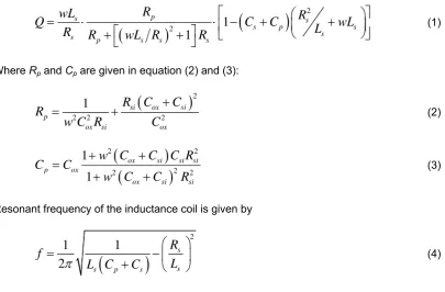
(4)Figure 2. The picture of current density vector Figure 3. The picture of magnetic induction intensity vector
Figure 4. The picture of magnetic induction intensity
Figure 5. The stress distribution of inductance coil substrate
3. Design and Manufacture of Inductance Coil
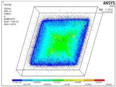
We adopt MEMS surface processing technology to design the inductance coil in this paper. The number of turns of the coil is 34, width of the coil conductor is 10 µm, and the coil conductor spacing is 10 µm. The fabrication technology process of the inductance coil is illustrated in Figure 6. Figure 7 is inductance coil sample photo.
Figure 6. The fabrication technology process of inductance coil
(a) Silicon wafer cleaning; (b) Surface oxidation; (c) Boron diffusion; (d) Lithography conductor hole; (e)Vapor aluminized film; (f) Etching aluminized film to form inductance coil
Figure 7. The photo of inductance coil sample
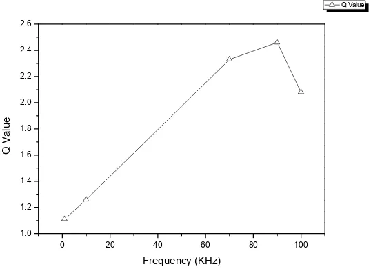
4. Experimental Results and Discussion
We get the inductance coil measured values and Q values in test condition of different frequencies by using precision LCR meter (TH2819A). The results of comparison between inductance coil theoretical value and the measured values are shown in Table 1. As can be seen from the Table, the measured value reached more than 22 μH, but the error is relatively large compared with the theoretical value. It is mainly due to ignorance of the internal down-lead, structure size of contact electrode, process conditions and precision of measuring instrument in the theoretical calculation.
(a)
(b)
(c)
(d)
(f)
(e)
SiO
Si
N
+high frequency, the energy loss in the silicon substrate increases with the frequency increased, resulting in the decrease of Q values.
0 20 40 60 80 100
1.0 1.2 1.4 1.6 1.8 2.0 2.2 2.4 2.6
Q Value
Frequency (KHz)
Q V
a
lu
e
Figure 8. The Q value curve of different frequencies
5. Conclusion
The inductance coil designed in this paper acts as the driving element of electromagnetic excitation resonant sensor, and the magnitude of magnetic field generated by coil is the decisive factor of drive capability. We adopted N-type high resistivity silicon wafer whose resistivity is 100Ω·cm to produce an inductance coil of 34 turns, and obtain a larger inductance value. By the magnetic inductance energy formula W=LI2/2, large inductance values can generate high magnetic field, causing the silicon membrane vibration.
At the same time, to reduce the thickness of porous array silicon membrane at the bottom of inductance coil to 5um, which can make the eddy current of substrate greatly reduce, playing an important role in inhibition of eddy current effect under high frequency. Through experimental demonstration, the inductance coil we design and manufacture in this paper is able to meet requirements of silicon micro pump, and has broad application prospects in microelectronics and micro system.
References
[1] Wen Dianzhong. Sensitivity Analysis of Junction Field Effect-Pressure Halltron. Review of Scientific Instrument. 1995; 66 (1): 251-255.
[2] Zhao Xiaofeng, Wen Dianzhong, Zhuang Cuicui, et al. Fabrication and Characteristics of the Magnetic Field Sensors Based on Nano-Polysilicon Thin-Film Transistors. Journal of Semiconductors. 2013; 34(3):036001(1-6).
[4] Yoon JB, Choi YS, Kim B, et.al. CMOS Compatible Surface-Micromachined Suspended-Spiral Inductors for Multi-GHz Silicon RFICs. IEEE Electron Device Letters. 2002; 23(10): 591-593.
[5] Gradolph, Friedberger, Muller, et.al. Environments on piezoresistive pressure sensorImpact of high-g and high vibration performance. Sensors and Actuators. A, Physical. 2009; 150(1): 69-77.
[6] Jiang Qi-feng Li Zheng-Fang. Modeling and Analysis of Spiral Inductors for Si-Based RFIC’s. Acta Electronic Sinica. 2002; 30(8): 1119-1121.
[7] Mengran Liu, Guojun Zhang, Zeming Jian, et.al. Design of Array MEMS Vector Vibration Sensor in the Location of Pipeline Internal Inspector. TELKOMNIKA Indonesian Journal of Electrical Engineering. 2014; 12(9): 6651- 6657.
[8] Zhang Zhi-yong, Hai Chao-He. High Q-Factor On-chip Spiral Inductors for Bulk Silicon CMOS RF IC’S. Microelectronics. 2003; 33(1): 15-18.
[9] Waugh WH, Gallacher BJ, Burdess JS. A High-Sensitivity Resonant Sensor Realized Through the Exploitation of Nonlinear Dynamic Behavior. Mess Sci Technol. 2011; 22(10): 105-202.
[10] Achmad Widodo, Latief Rozaqi, Ismoyo Haryanto, et.al. Development of Wireless Smart Sensor for Structure and Machine Monitoring. TELKOMNIKA Telecommunication Computing Electronics and Control. 2013; 11(2): 417-424.