148
Abstract—The Space Vector Pulse Width Modulation (SVPWM) is possibly the best among all the PWM techniques for variable frequency drive applications. Unfortunately, the modulation algorithm is mainly implemented with software based on microcontroller or digital signal processors (DSP). These are software-based technique purely and obviously not an ideal solution. Employing Field Programmable Gate Array (FPGA) to realize SVPWM strategies provides advantages that it is considered as an appropriate solution to boost system performance of an SVPWM algorithm. Moreover, although in the literatures the implementation for three-phase SVPWM based on FPGA is not lacking, however all these designs are based on the conventional SVPWM without considering hardware-resource saving and not simple. This paper present a simple realization of 5-segment discontinuous SVPWM with a difference approach based on FPGA, in which the judging of sectors and the calculation of the firing time to generate the SVPWM waveform is simple, and also the switching losses is low. The proposed discontinuous SVPWM has been designed and successfully implemented by using APEX20KE Altera FPGA considering hardware-resource saving and has successfully driven a three phase inverter system with induction machine 1.5 kW as load.
Index Terms—space vector, pulse width modulation, discontinuous SVPWM, FPGA, simple realization
I. INTRODUCTION
The Space Vector Pulse Width Modulation (SVPWM) method is an advanced PWM method and it is possibly the best among all the PWM techniques for variable frequency drive applications. In recent years, this method gradually obtains widespread applications in the power electronics and the electrical drives, because of its superior performance characteristics. Compared to the Sinusoidal Pulse Width Modulation (SPWM), SVPWM is more suitable for digital implementation and can increase the obtainable DC voltage utilization ratio very much. Moreover, it can obtain a better voltage total harmonic distortion factor [1-4]. Up to now, its theories and algorithms have been well developed and applied more widely with the progress of power electronics.
Manuscript received July 13, 2009.
Tole Sutikno is with the Department of Electrical Engineering, Universitas Ahmad Dahlan (UAD), Yogyakarta, Indonesia and Department of Energy Conversion, Universiti Teknologi Malaysia (UTM), Johor, Malaysia, e-mail: [email protected] or [email protected]
Auzani Jidin is with the Department of Power Electronics and Drives, Universiti Teknikal Malaysia Melaka (UTeM), Melaka, Malaysia, e-mail: [email protected] or [email protected]
Mohd Farriz Basar is with the Department of Power Electronics and Drives, Universiti Teknikal Malaysia Melaka (UTeM), Melaka, Malaysia, e-mail: [email protected] or [email protected]
In most engineering practice, the SVPWM algorithm is mainly implemented with software based on microcontroller or digital signal processors (DSP) are widely adopted. They perform control procedure sequentially by exploiting their mathematically oriented resources. That is the instructions of different procedures are executed one after the other. Thus, the purely software-based technique is not an ideal solution. Employing Field Programmable Gate Array (FPGA) to realize SVPWM strategies provides advantages such as rapid prototyping, simpler hardware and software design, and higher switching frequency. Differ from software implementation; FPGA performs the entire procedures with concurrent operation (parallel processing by means of hardware mode and not occupying) by using its reconfigurable hardware. For its powerful computation ability and flexibility, an FPGA is considered as an appropriate solution to boost system performance of a digital controller including an SVPWM algorithm [2, 5-8].
However, this conventional SVPWM suffers from the drawbacks like computational burden, inferior performance at high modulation indices and high switching losses of the inverter. Hence to reduce the switching losses and to improve the performance in high modulation region, several discontinuous SVPWM methods have been proposed [9-11]. Although in the literatures the implementation for three-phase conventional SVPWM and discontinuous SVPWM based on FPGA is not lacking, however all these designs are based on the conventional SVPWM without considering hardware-resource saving. In this paper, we design and implement a FPGA based SVPWM with a difference approach, in which the judging of sectors and the calculation of the firing time to generate the SVPWM waveform is simple, and also the switching losses is low. In this paper, a novel 5-segment discontinuous SVPWM design based on the basic idea from [4] and [12] is proposed. This scheme is hoped that it has lower switching losses, simpler algorithm and can be implemented easily based on APEX20KE Altera FPGA.
II. THE PRINCIPLES OF CONVENTIONAL SVPWM The main aim of any modulation technique is to obtain variable output having a maximum fundamental component with minimum harmonics and less switching losses. The SVPWM technique is more popular than conventional technique. This technique was originally developed as a vector approach to pulse width modulation (PWM) for three phase inverter [1]. It is a more sophisticated technique for generating sinusoidal wave that provides a higher voltage to
Simple Realization of 5-Segment Discontinuous
SVPWM Based on FPGA
149 the motor with lower total harmonic distortion. It confines space vector to be applied according to the region where the output voltage vector is located.
SVPWM refers to special switching scheme of the six power transistor of a three phase power converter. It is based on fact that there are only two independent variables in a 3-phase voltage system. We can use orthogonal coordinates to represent the 3-phase voltage in the phasor diagram. A three-phase-voltage vector can be expressed as:
V
ref =
0 0 0 2 3 2 3 0 2 1 2 1 1 3 2 C B A v v v V V (1)
In the SVPWM scheme, the 3-phase output voltage is represented by a reference vector which rotates at an angular
speed of ω =2π f. The task of SVM is to use the combinations of switching states to approximate the reference vector, V
ref. To approximate the locus of V
ref, the eight possible switching states of the inverter are represented as 2 null vectors and 6 active vectors. The operating states and corresponding vectors are listed in Table I.
TABLE I: SWITCHING STATE OF THE 2-LEVEL INVERTER Space vector Switching state On switches S
i Zero
vector V
7 111 1, 3, 5
V
0 000 2, 4, 6
Active vector
V
1 100 1, 2, 4
V
2 110 1, 3, 6
V
3 010 2, 3, 6
V
4 011 2, 3, 5
V
5 001 2, 4, 5
V
6 101 1, 4, 5
These vectors (V
1~V6) can be used to frame the vector plane, which is illustrated in Figure1. The rotating reference vector can be approximated in each switching cycle by switching between the two adjacent active vectors and the zero vectors. In order to maintain the effective switching frequency at a minimal value, the sequence of the toggling between these vectors is organized in such way that only one leg is affected in every step.
A. Identification of the sector
The sector judgment and application time of active vector for all SVM strategies are the same. Based on Figure 1 (a), it is obvious that the sector number is determined by the angle of the reference vector. The identification of k can be
generally in αβ coordinates deal with by the appropriate
boundary condition according to Table II.
B. Determination of the duration of active vectors
For digital control application, the reference inputs are sampled in a regular sampling interval to determine the switching duration of the active vectors. That it, any reference vector inside the hexagon can be obtained two adjacent active vector (V
k ,Vk+1). Then, Vref can be expressed as functions of V
k and Vk+1 by the following equation:
(a)
(b)
Fig. 1 Vector plane frame; (a) space voltage vectors, (b) Decomposition V ref with V
k and Vk+1 (e.g., in sector I)
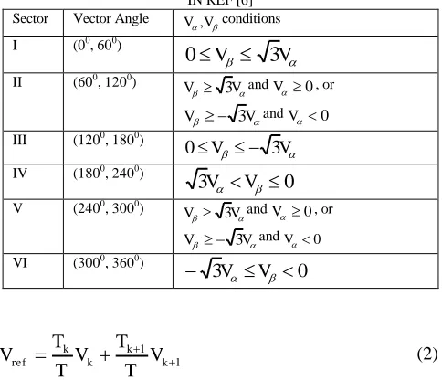
TABLE II: CRITERION OF THE SECTOR IDENTIFICATION IN REF [6]
Sector Vector Angle V,Vconditions
I (00, 600)
V
V
3
0
II (600, 1200)
V
V 3 and V0, or
V
V 3 and V0 III (1200, 1800)
V
V 3
0
IV (1800, 2400)
0 3V V V (2400, 3000)
V
V 3 and V0, or
V
V 3 and V0 VI (3000, 3600)
0 3
V V
1 1 k k k k ref V T T V T T V (2) Where T
k and Tk+1 are the dwell time of Vk and Vk+1 during each sampling period (T) each sampling period, respectively, and k is the sector number corresponding to the reference location. For example in sector I, k=1, vector V
1 activates lasting for T
1, and V2 activates lasting for T2 during T. The principle is similar in all sector of the six sectors, therefore Figure 1 (b) highlights the relation for sector I only.
Considering that magnitude of non zero space satisfies ||V
150 following equations:
1 0
1 ( 1))
3 cos( ))
1 ( 3 sin( 3
) 3 cos( )
3 sin( 3
k k dc k
dc k
T T T T
V k V
k T
V T
V k V
k T V T
(3)
Where V
dc is the dc-link voltage of the inverter, and T0 is the switching duration of a zero vector in each sampling period. Suppose the reference is keeping a circular trajectory, the T
0>0, the output voltage is a regular sinusoidal in linear modulation. As (3), it is theoretically simple but it is obvious that this algorithm required complicated computations with trigonometric function.
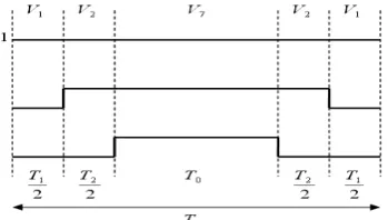
C. Switching sequence (switching pattern)
This SVPWM strategy aims to minimize harmonic distortion in the current by selecting the appropriate switching vectors and determining of their corresponding dwelling widths. The flux produced by the reference voltage vector in a SVPWM switching period is a combination of each individual flux resulted by corresponding voltage vector. There are many switching pattern to implementation SVPWM. The choice of the null vector determines the SVPWM scheme. There are a few options: the null vector V0 only, the null vector V7 only, or a combination of the null vectors.
Fig. 2 SVPWM Pattern I (conventional 7-segment switching sequence) of the sector I
Fig. 3 SVPWM Pattern II (other conventional 7-segment switching sequence) of the sector I
The equivalent PWM waveforms, which produce the same average flux, may consist of various combinations of the basic vectors. However, the sector judgment and application time of active vector for all SVM strategies are the same. Based on [5, 11-13] can be created some switching patterns.
Figure 2 and 3 show two different 7-segment algorithm switching sequence patterns of the sector I, while Figure 4 Figure 5 show two different 5-segment algorithm switching sequence patterns of the sector I. Only null vector V7 and null vector V0 is used in each cycle respectively. Its sequences are symmetrical too. This scheme lowers the switching times than pattern I. Moreover, the algorithm can be implemented easily by DSP or FPGA.
Fig.4 SVPWM Pattern III (5-segment switching sequence) of the sector I
Fig. 5 SVPWM switching Pattern IV (other 5-segment switching sequence) of the sector I
III. A SIMPLE REALIZATION METHOD OF SVPWM ALGORITHM
Different from the conventional principle of SVPWM algorithm, this section will present symmetrical 5-segment discontinuous switching sequence to replace symmetrical 7-segment continuous switching sequence in conventional SVPWM, new judge method of sectors, and new SVPWM generating method based on calculation of the duration of active vectors.
A. Proposed SVPWM switching Pattern (5-segment
discontinuous switching sequence)
151 switching losses.
B. Proposed identification of the sector
There are many kinds of methods to judge the sector that the reference space voltage vector lies in. Zhi-pu [14]
compares the reference space vector’s angle with 00 , 600, 1200, 1800, 2400, and 3000 to obtain the number of the sector that the Vref in. In other references, Yu [15], Jiang [7] and Xing [16] obtain the sector number by analyzing the relationship between
V
andV. To determine the sector, they calculate the projectionsV
a,V
bandV
cofV
andVin (a,b,c) plane by using inverse Clark transformation, as follow: 2 3 2 3 V V V V V V V V c b a (4)Then, based on equation (), they calculate N=sign(Va) + 2*sign(Vb) + 4*sign(Vc). Map N to the actual sector of the output voltage reference by referring to Table III.
TABLE III: MAP N TO THE ACTUAL SECTOR OF THE OUTPUT VOLTAGE REFERENCE
N 1 2 3 4 5 6
sector 2 6 1 4 3 5
Fig.6 The plotting of
V
,
3
V
,
3
V
waveTABLE IV: THE PROPOSED IDENTIFICATION OF THE SECTORS Sector Vector Angle
V > 0 V> 3V V>
V 3
I (00, 600) 1 0 1
II (600, 1200) 1 1 1
III (1200, 1800) 1 1 0
IV (1800, 2400) 0 1 0
V (2400, 3000) 0 0 0
VI (3000, 3600) 0 0 1
1: satisfy, 0: not satisfy
In [17], Zeliang has adopted the new intermediate vector
X
and X that it define as
V
X 2 3
and X 3V as
decompose the conventional SVPWM, which will properly counteract the redundant calculations to identify sector location, but it imported the complicated matrix calculations. In this paper, based on analyzing the principle of SVPWM in [7, 15-17] and to reduce burden of computation, a new method to determine the sectors of voltage vectors based on comparison between
V
,
3
V
,
3
V
and 0 as shown in Figure 6 is proposed. Through the comparison, we can determine the sectors of voltage vectors as shown in Table IV.C. Determination of the duration of active vectors
The space vector technique allows to synthesizing a desired vector V
ref from two adjacent actives, Vα and Vβ (among V
1 and V2, as shown in Figure 1) during time interval, T
a and Tb. The null vectors (V0 and V7) are also applied to reduce the inverter switching frequency. In the proposed design, only one null vector is inserted in a PWM period, only V
7 for odd sector and only V0 for even sector.
V
ref=Vα + jVβ=
T
T
V
T
T
a2
b2
(5)
0
2
T
T
T
T
b
a
(6)Hence, the half PWM period T is composed by the switching time T
a, Tb and T0. The total time of the null vectors can be expressed as
b
a
T
T
T
T
2
0 (7)
TABLE V: THE SWITCHING TIME OF THE ACTIVE VECTOR FOR EACH SECTOR
Sector T
a Tb Ta+Tb
I dc dc V V V V T 3 4
3
dc V V T 3 2 4 3 dc dc V V V V T 3 4
3
II dc dc V V V V T 3 4
3
dc dc V V V V T 3 4
3
dc V V T 3 2 4 3 III dc V V T 3 2 4 3 dc dc V V V V T 3 4
3
dc dc V V V V T 3 4
3
IV dc dc V V V V T 3 4
3
dc V V T 3 2 4 3 dc dc V V V V T 3 4
3
V dc dc V V V V T 3 4
3
dc dc V V V V T 3 4
3
dc V V T 3 2 4 3 VI dc V V T 3 2 4 3 dc dc V V V V T 3 4
3
dc dc V V V V T 3 4
3
152
D. Proposed SVPWM switching sequence generating
method based on calculation of the duration of active vectors
In this paper, with refer to equation
x
T
m
y
2
inFigure 7, the PWM generating for odd sector are realized through comparison between triangle and
T
a, and between triangle andT
a
T
bwith other switching is set equal to 1; while for even sector, the PWM generating are realized through complement of comparison between triangle andT
a, and complement of comparison between triangle andb
a
T
T
with other switching is set equal to 0. For example,in sector I if x=Ta=
2
0
T
then
)
2
(
2
T
0T
m
y
and ifx=Tb=
2
1
T
then
)
2
(
2
T
1T
m
y
.Fig.7 Proposed SVPWM switching sequence generating method
For more simplicity of circuit design, in this paper the term
T m 2
is set equal to 1, so if x= 2
0
T =T
a then y= 2
0
T =T
a, and
if x=
2
1
T then y=
b
T T
2
1 . Obviously if x=
b
a T
T T T
2 2
1
0 then
y=
b
a T
T T T
2 2
1
0 . Therefore, the PWM generating for Sb and Sc channels in sector I can be obtained through comparison between triangle and
T
a, and between triangle andT
a
T
b respectively and Sa Channel is set equal to 1. Moreover, the PWM generating in other sectors can be obtained in the similar way.IV. FPGA IMPLEMENTATION OF A PROPOSED NOVEL SVPWM
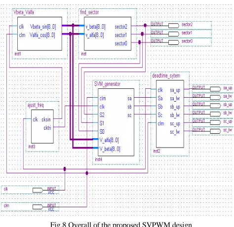
In previous section, the principle of SVPWM is analyzed. In this section FPGA implementation of a proposed novel
SVPWM will be presented. Overall of the proposed SVPWM design is shown in Figure 8. This top module can be sub divided into 5 sub modules, namely ajust_freq, Vbeta_Valfa,
find_sector, SVM_generator and deadtime_sytem module.
A. Adjust of Carrier and Fundamental Frequency Module
In this module, the main clock frequency is designed to connect L6 pin at APEX20KE Altera FPGA board system. It is 33.33 MHz dedicated clock generator in this board. The clocking system to adjust carrier and fundamental frequency is done in this module. In this research, carrier frequency is set to 20 kHz and in temporary, fundamental frequency is set fixed to 50 Hz. It to get carrier and fundamental frequency is done through clock dividing.
Fig.8 Overall of the proposed SVPWM design
For example, because of the triangle signal generator design in this research is sampled 32 times per period, then it to get 20 kHz is done through dividing of the main clock generator above with 13 (33.33MHz:(13x32)=20 kHz). The fundamental frequency also can be gotten through similar dividing.
B. Vα and Vβ Module
In this research, Vα and Vβ is generated using sine and cosine function through look up table (LUT) with memory mapping 360 addresses. The lower, base, and higher number of sine and cosine function is represented with 96, 224 and 352 respectively in 9 unsigned bits. The design of Vα and Vβ
153 Fig.9 Vα and Vβ Module
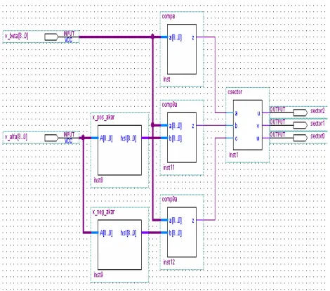
C. Sector Finder Module
Due to existing different switching time equations, the reference voltage sector knowledge is necessary. The SF module is responsible judging the reference vector sector and does it using Table 2 above. As Figure 10, the “x_pos_akar”
and “x_neg_akar” module are used to multiply between
V
with3
andV
with
3
respectively. Then, these results of operation are compared with V through“comp9a” module that it is written is VHDL code, and in
other hand V is compared with zero through “compa”
module. It to determine number of sector is done with simplification of truth table that it is developed from the results of comparison above, as shown in Table VI through
“csector” module.
Fig.10 Sector finder (SF) module
TABLE VI: CONVERSION OF RESULT OF COMPARISON BETWEEN
V V
V , 3 , 3
AND 0 TO DETERMINE SECTOR Sector Vector Angle Input Ouput (S2S1S0)
I (00, 600) 101 001
II (600, 1200) 111 010
III (1200, 1800) 110 011
IV (1800, 2400) 010 100
V (2400, 3000) 000 101
VI (3000, 3600) 001 110
D. Three phase SVPWM signal generator module
The overall of three phase SVPWM signal generator module is shown in Figure 11. This module can be sub divided into 4 sub modules, namely Triangle, Duration_Ta,
Duration_TaTb, and SVM pattern module. Triangle module
is functioned as triangle signal generator. In this research, one period of triangle signal generator is sampled 32 times, and then it is represented in the digital number 9 unsigned bit, with lower (in this case is same with base number) and higher number each are 224 and 352 respectively. Due to
Duration_Ta and Duration_TaTb module, these modules are
digital solution of each second and fourth column respectively. And SVM pattern module as the last module is functioned as SVPWM switching sequence generating as it is described in section 3.4 and it is illustrated in Figure 7.
Fig.11 Three phase SVPWM signal generator module
V. RESULTS AND DISCUSSIONS
A. Simulation
This mode is based on the Quartus II, the parameters are listed as follows: V
dc/T=1, switching frequency has been tried at 2.5 and 20 kHz, and fundamental frequency 50 Hz. The compilation report of proposed SVPWM generator design is shown in Figure 12 (a), and it more detail for each module in Figure 12 (b). It can be seen that the design requires 520 logic elements and 9.216 memory bits.
Figure 13 show simulation results of the proposed SVPWM generator. These results verify by simulation that the proposed design runs with the desired.
B. Experimental
154 implementation based on FPGA (programmer level). In this research, the proposed SVPWM generator design with some carrier frequency has programmed to APEX20KE Altera FPGA successfully.
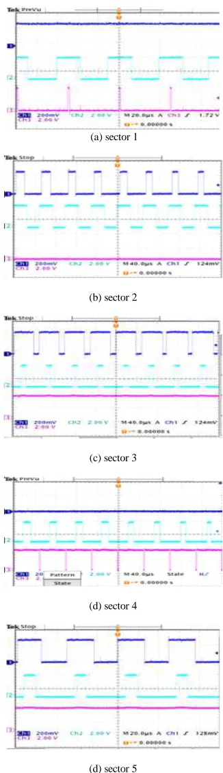
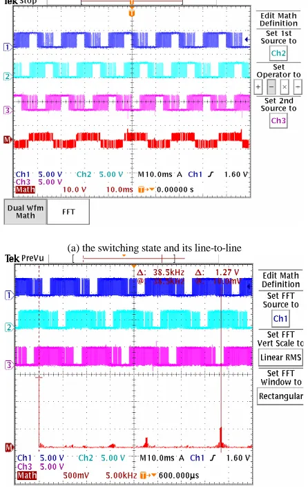
The sequence of switching state in each sector and the dead time with 2 µs that they also has been done successfully as shown in Figure 14 and 15 respectively. Inherently, Figure 16 shows hardware implementation of proposed SVPWM generator at carrier frequency 20 kHz. The first, second and third channel at Figure 16 (a) and (b) is each Sa, Sb, and Sc switching state respectively, otherwise fourth channel is each (Sa-Sb) line-to-line switching state and its frequency spectrum respectively. The harmonics due to the 20 kHz switching frequency are clearly visible in Figure 16 (b). The results above have proved that the proposed SVPWM generator has realized in hardware platform based on FPGA and has run with desired.
(a) Compilation report
(b) The using of FPGA resource in detail
Fig.12 The using of FPGA resource of proposed SVPWM generator design
Fig 13. The simulation results of the proposed SVPWM generator Inherently, Figure 16 shows hardware implementation of proposed SVPWM generator at carrier frequency 20 kHz. The first, second and third channel at Figure 16 (a) and (b) is
each Sa, Sb, and Sc switching state respectively, otherwise fourth channel is each (Sa+Sb) line-to-line switching state and its frequency spectrum respectively. The harmonics due to the 20 kHz switching frequency are clearly visible in Figure 16 (b). The similar condition is shown in Figure 17. In this case, carrier frequency is set to 40 kHz; although the testing result as Figure 17 (b) showed that it is detected 38.5 kHz (error 3.75%). These results above have proved that the proposed SVPWM generator has realized in hardware platform based on FPGA and has run with desired.
(a) sector 1
(b) sector 2
(c) sector 3
(d) sector 4
155 (e) sector 6
Fig.14 The sequence of switching state in each sector
(a) The dead time of Sa switching state in sector 2
(b) The zoomed dead time of Sa switching state in sector 2
Fig.15 The dead time of proposed SVPWM generator
(a) The switching state and its line-to-line
(b) The signal gating and its frequency spectrum
Fig.16 Hardware implementation of proposed SVPWM generator at carrier frequency 20 kHz.
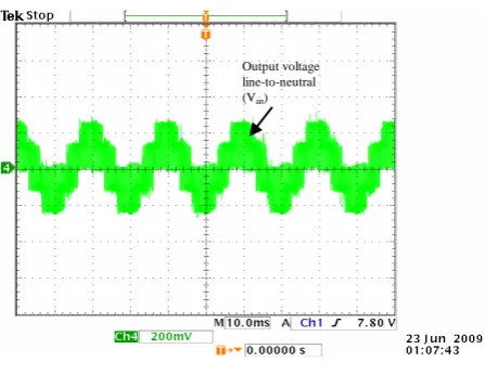
To test the performance of FPGA based proposed SVPWM generator design, this design has been used to drive a three phase inverter system with induction machine 1.5 kW as load. Figure 18 shows the practical result for output stator current (Ia), output phase-to-phase voltage (Vab), frequency spectrum and output voltage line-to-neutral (Van). This figure shows that the practical result obtained from test-rig is in good agreement.
(a) the switching state and its line-to-line
(b) The signal gating and its frequency spectrum
Fig.17 Hardware implementation of proposed SVPWM generator at carrier frequency 40 kHz.
156 and has run with desired.
VI. CONCLUSION
This paper presents the design and simple realization of FPGA based a novel 5-segment discontinuous SVPWM with a difference approach, in which the judging of sectors and the calculation of the firing time to generate the SVPWM waveform is simple, and also the switching losses is low. The proposed SVPWM scheme has been designed and successfully implemented by using APEX20KE Altera FPGA considering hardware-resource saving. It is simple and without compute the angles of each sector to determine number of sector and the commutation pattern and that it has programmed to FPGA successfully in some carrier frequency until 40 kHz. Moreover, this scheme has simple algorithm that it can be implemented easily based on FPGA without computational burden and has successfully driven a three phase inverter system with induction machine 1.5 kW as load.
(a) output current and voltage
(b) frequency spectrum
(c) output voltage line-to-neutral
Fig.18 The performance of FPGA based proposed SVPWM generator design.
REFERENCES
[1] H. W. van der Broeck, H. C. Skudelny, and G. V. Stanke, "Analysis and realization of a pulsewidth modulator based on voltage space vectors," Industry Applications, IEEE Transactions on, vol. 24, pp. 142-150, 1988. [2] C. S. Moreira, R. C. S. Freire, E. U. K. Melcher, G. S. Deep, S. Y. C. Catunda, and R. N. C. Alves, "FPGA-based SVPWM trigger generator for a 3φ voltage source inverter," in Instrumentation and Measurement Technology Conference, 2000. IMTC 2000. Proceedings of the 17th IEEE, 2000, pp. 174-178 vol.1.
[3] B. K. Bose, Modern Power Electronics and AC Drives. New Jersey: Prentice-Hall PTR, 2002.
[4] A. M. Trzynadlowski, R. L. Kirlin, and S. Legowski, "Space vector PWM technique with minimum switching losses and a variable pulse rate," in Industrial Electronics, Control, and Instrumentation, 1993. Proceedings of the IECON '93., International Conference on, 1993, pp. 689-694 vol.2. [5] T. Ying-Yu and H. Hau-Jean, "FPGA realization of space-vector PWM control IC for three-phase PWM inverters," Power Electronics, IEEE Transactions on, vol. 12, pp. 953-963, 1997.
[6] Z. Zhaoyong, L. Tiecai, T. Takahashi, and E. Ho, "Design of a universal space vector PWM controller based on FPGA," in Applied Power Electronics Conference and Exposition, 2004. APEC '04. Nineteenth Annual IEEE, 2004, pp. 1698-1702 Vol.3.
[7] S. Jiang, J. Liang, Y. Liu, K. Yamazaki, and M. Fujishima, "Modeling and cosimulation of FPGA-based SVPWM control for PMSM," in Industrial Electronics Society, 2005. IECON 2005. 31st Annual Conference of IEEE, 2005, p. 6 pp.
[8] Y. Guijie, Z. Pinzhi, and Z. Zhaoyong, "The Design of SVPWM IP Core Based on FPGA," in Embedded Software and Systems Symposia, 2008. ICESS Symposia '08. International Conference on, 2008, pp. 191-196. [9] Z. Keliang and W. Danwei, "Relationship between space-vector
modulation and three-phase carrier-based PWM: a comprehensive analysis [three-phase inverters]," Industrial Electronics, IEEE Transactions on, vol. 49, pp. 186-196, 2002.
[10] K. S. Gowri, T. B. Redd, and C. S. Babu, "Novel Space Vector Based Generalized Discontinuous PWM Algorithm for Induction Motor Drives," ARPN Journal of Engineering and Applied Sciences, vol. 4 no.1, February 2009.
[11] W.-F. Zhang and Y.-H. Yu, "Comparison of Thre SVPWM Strategis," Journal of Electronic Science and Technology of China, vol. 5 no.3, pp. 283-287, September 2007.
[12] Z. Yu, "Space-Vector PWM With TMS320C24x/F24x Using Hardware and Software Determined Swithing Patterns," Texas Instruments Application Report SPRA524, March 1999.
[13] C. Bharatiraja, T. B. Prasad, and R. Latha, "Comparative Realization of Different SVPWM Schemes in Linear Modulation Using FPGA," in IEEE Region 8 Sibircon, 2008, pp. 164-168.
[14] Z. Zhi-pu, "Design and Realization of Space Vector PWM Based on SG," Drive and Control, vol. 7, pp. 29-32, 2005.
[15] F. Yu, X. Yan, and H. Yuwen, "A fast algorithm for SVPWM in three phase power factor correction application," in Power Electronics Specialists Conference, 2004. PESC 04. 2004 IEEE 35th Annual, 2004, pp. 976-979 Vol.2.
[16] S. Xing and K.-Y. Zhao, "Research on A Novel SVPWM Algorithm," in Industrial Electronics and Applications, 2007. ICIEA 2007. 2nd IEEE Conference on, 2007, pp. 1869-1872.
Fundamental
frequency Output current Ia
Output voltage Vab
Carrier frequency 38.5 kHz Output
voltage Vab
Output current Ia
157 [17] S. Zeliang, T. Jian, G. Yuhua, and L. Jisan, "An Efficient SVPWM
Algorithm With Low Computational Overhead for Three-Phase Inverters," Power Electronics, IEEE Transactions on, vol. 22, pp. 1797-1805, 2007.
Tole Sutikno (M’07 IEEE) received his B.Eng. degree in electrical engineering from Diponegoro University (UNDIP), Semarang, Indonesia, his M.Eng. degree in Power Electronics from Gadjah Mada University UGM), Yogyakarta, Indonesia, in 1999 and 2004, respectively. Since 2001 he has been a lecturer in Electrical Engineering Department, Universitas Ahmad Dahlan (UAD), Yogyakarta, Indonesia. He is currently PhD Student in Energy Conversion, Universiti Teknologi Malaysia (UTM), Johor, Malaysia. His research interests include the field of power electronics, motor drive systems and field programmable gate array (FPGA) applications. Email: [email protected] or [email protected]
Auzani Jidin (M’07 IEEE) received his B.Eng. degree and M.Eng. degree in Power Electronics and Drives from Universiti Teknologi Malaysia (UTM), Johor, Malaysia in 2002 and 2004, respectively. He is currently PhD Student in the same University. He is currently lecturer at Power Electronics and Drives Department, Universiti Teknikal Malaysia Melaka (UTeM), Melaka, Malaysia. His research interests include the field of power electronics, motor drive systems, field programmable gate array (FPGA) and digital signal processing (DSP) applications. Email: [email protected] or [email protected]