Application of statistical method to investigate the effects of design
parameters on the performance of microring resonator channel
dropping
fi
lter
Hazura Haroon*,†, Sahbudin Shaari, P.S Menon, Hanim Abdul Razak and Mardiana Bidin
Institute of Microengineering and Nanoelectronics (IMEN), Universiti Kebangsaan Malaysia (UKM), 43600 UKM Bangi, Selangor, Malaysia
ABSTRACT
Microring resonator (MRR)-based channel droppingfilters have been extensively explored because of the high quality factor, compact size, and easy integration of fabrication. In order to design an excellent MRR wavelengthfilter, optimization of the design parameters are essential. In this paper, the design trade-off of MRR-based channel dropping filter was statistically studied by employing the Taguchi method. Four control factors considered were width of rings and channels, radii of the microring, upper rib waveguide height, and gap size. The analysis of variance was adopted to analyze significant trends that occurred on the free spectral range (FSR) and insertion loss (IL) performance under different sets of control factor combinations. The best parametric combination of control factors was identified in order to achieve a balance performance between large FSR and low IL using Finite-Difference Time Domain (FDTD) simulation by RSoft Inc. After optimization, the value of FSR and IL obtained was 17 nm and 0.245 dB, respectively. Confirmation tests were carried out to verify the optimized parametric combinations and a new parametric combina-tion considering both outputs were 16 nm and 0.215 dB. The optimal combinacombina-tions were 6mm ring radius with the
separation gap of 50 nm and 350 nm350 nm rib waveguide cross section. Copyright © 2013 John Wiley & Sons, Ltd.
Received 11 May 2012; Revised 27 February 2013; Accepted 28 February 2013
KEY WORDS: silicon photonics; microring resonator; optical wavelength filter; Taguchi method; analysis of variance (ANOVA)
1. INTRODUCTION
Rapid development in the high-index-contrast (HIC) technology has resulted in the demonstrations of
various microring resonator (MRR)-based devices, including wavelength filter [1], multiplexer [2],
sensors [3], and modulators [4]. MRRs have attracted extensive research due to their advantages of high-quality factor, simple structure, as well as compact size.
Microring resonators were first proposed as integrated optical wavelength filters by Marcatili in 1969 [5]. By utilizing the HIC characteristics of silicon dioxide, a very wide free spectral range (FSR) can be realized with the possibility for the creation of very densely photonic integrated circuits systems. MRRs are ideal devices for developing almost every fundamental block in wavelength
division multiplexed (WDM) networks. MRR-based wavelength filters or channel dropping filters
are recently applied tofilter out the required channel from a WDM signal. MRR channel droppingfilter offers high wavelength selectivity, low propagation loss, and extremely small footprints [6]. A major
challenge in implementing such high efficiency MRR channel dropping filter is to ensure large
*Correspondence to: Hazura H., Institute of Microengineering and Nanoelectronics (IMEN)Universiti Kebangsaan Malaysia (UKM)43600 UKM Bangi, Selangor, Malaysia.
†E-mail:[email protected]
bandwidth or FSR, low loss, box-likefilter response, and high out-of-band signal rejection is attained. As it is well-known, in WDM systems, it is important to have a very wide FSR so that it is capable to accommodate a huge number of information and users. Our work attempted to design a large FSRfilter with an acceptable low loss. The largest FSR value of MRRfilter reported so far is 32 nm at 1.55mm
telecommunication wavelengths, fabricated on silicon-on-insulator (SOI) platform [6], having the ring radius of 2.5mm. However, the loss produced was large (4.5 dB/mm). The results show that there is a
trade-off between large FSR and low propagation loss. Hence, a study to analyze the balance between both characteristics is crucial. In real applications, the overall device performance relies upon many parameters and it is difficult to determine which parameter has the most significant effect on the device performance. Therefore, many efforts were undertaken toward the optimization of design parameters to ensure the reliability of WDM systems.
To solve this, a systematic approach introduced by Genichi Taguchi based on orthogonal array (OA) experiments was applied. The Taguchi method tremendously reduces the number of experiments to be conducted and the impact of varying multiple controllable parameters to the device performance can be thoroughly investigated. This will aid researchers to achieve the best combination of design parameters or control factors to ensure an optimum quality of the MRR-basedfilter [7, 8]. Optimization of design parameters is the key step in the device modeling because it tremendously reduces the total manufacturing cost mainly because of fabrication, as well as research and development.
In this paper, we present results from numerical simulations which was used to characterize key optical design parameters of a laterally coupled SOI-based MRR channel droppingfilter using FullWAVE software by RSoft Inc. FullWAVE is a simulation engine that ideal for the design of complex photonic devices. The simulation allows analysis of devices, such as photonic bandgaps and MRRs, that cannot be modeled with techniques as the efiicient beam propagation method.
The FSR and IL of channel droppingfilters are very much dependent on the ring radii, the separation gap between the input/output waveguide and ring waveguide, as well as the waveguide cross-section. In order to obtain an improved wavelengthfiltering, we perform the optimization of these parameters using the Taguchi method. To the best of the authors’knowledge, this study is thefirst of its kind to profoundly analyze the effect of control and noise factor in the modeling of a SOI-based MRR channel droppingfilter prior to actual fabrication.
2. DEVICE DESCRIPTION AND THEORY
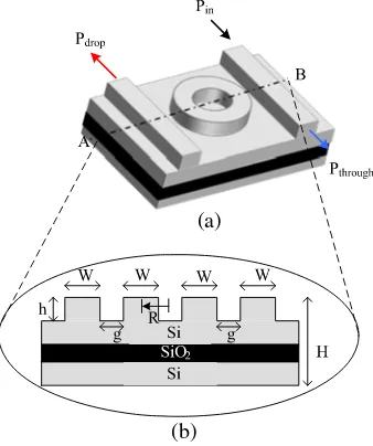
The MRR channel droppingfilter can be realized by a simple topology composed of double straight
waveguides coupled to a single microring as depicted schematically in Figure 1. R is the ring radius,
(a)
(b)
g is the separation gap between straight and ring waveguide, W is the waveguide width, and h is the upper rib height. These four paramaters are the studied control factors in this paper. The straight waveguides or bus waveguides serve as input and output channels for the evanescent waves.
The rib dimensions are chosen in order to obtain a single mode behavior. The slab waveguide has a dimension of 0.7mm on top of a buried oxide layer. SOI platform has been selected because of its
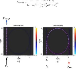
high-index contrast, low cost, and compatibility with available facility [9, 10]. The resonance behavior can be explained by Figure 2, where it shows the on-resonance and off-resonance states for thefirst order of SOI MRRfilter. At off-resonance state, input signal bypasses the ring and is emitted at the through port (Figure 2 (a)); whereas at the on-resonance state, light is coupled to the ring and is directed to the through port, depending on the resonance frequency (Figure 2 (b)).
An example of the simulated transmission response observed at the drop port is depicted in Figure 3. Theoretically, power transmission outputs at the through port,Pthrough, and the drop port,Pdropfor the first-orderfilter can be predicted by [11]
Pthrough¼
l lo
ð Þ2þ FSR 4p 2 k2
p
2
l l0
ð Þ2þ FSR 4p
2
2k2þk2 p
2 (1)
Figure 2. Resonant condition of microring resonatorsfilter.
Pdrop¼
wherelois the resonant wavelength,k2is the power coupling coefficient between the bus waveguide
and the resonator, andk2pis the propagation power loss coefficient per round trip in the MRR.
To characterize the device, TE-light was launched into the input port and the response at the output port was scanned from optical wavelengths of 1540–1570 nm. From the output power observed, the IL and FSR were calculated. Low IL is demanded in WDM network to scale down the number of amplifiers employed and hence, reduce the overall network system cost. IL is the ratio between the power received and the input power in dB, whereas the FSR can be calculated by observing two consecutive peaks as shown in Figure 3, or using equation [2] as follows:
FSR l0
2
ngð ÞLl eff
(3)
wherengis the group refractive index andLeffis the effective length.
3. TAGUCHI METHOD
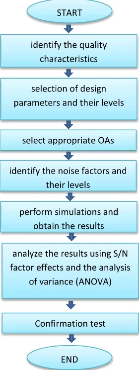
In this study, we apply the Taguchi method based on OA to study the variation effect of four design parameters (R, g, W, h) on FSR and IL. OA is the matrix of numbers arranged in columns and rows. The steps involved are summarized as shown in Figure 4.
The Taguchi quality characteristics studied in this research was signal-to-noise ratio (SNR) of
‘larger the better’for the FSR and SNR of ‘smaller the better’for IL because we aim to produce a device that can accommodate huge bandwidth (FSR) with a satisfactory low loss.
The SNR was computed to predict the effect of each design parameters on the targeted performance and the higher value of S/N is requisite. For‘larger the better’, the SNR,can be calculated by
¼ 10 log101
wherenis the number of test andyiis the simulation value of FSR. Whereas for‘smaller the better’,
SNR,can be calculated by
¼ 10 log101
whereY1toYnis the value of the insertion loss.
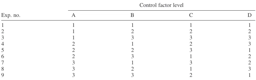
An L9 (3
4
) array, SNR (S/N) and analysis of variance were employed for the optimization and analysis of the FSR and IL. A total of four design parameters or control factors denoted as A (Rib radius, R), B (separation gap, g), C (rib height, h), and D (waveguide width, W) were selected as shown in Table 1. Theoretically, by reducing the ring radius, FSR will be enhanced. Because of fabrication tolerances, we selected the ring radii in the ranges of 6–12mm. Varying the separation gap between
the actual fabrication. The Taguchi method is suggested in this study, where the optimum combinations of selected parametric design parameters can be obtained.
The Taguchi L9OA performed in this study is shown in Table 2. Noise factors or uncontrollable
design parameters have been selected in the analysis with three levels each (refer Table 3). They are denoted as R (surface roughness) and S (slope angle). Typically, the roughness of silicon surface generated after the lithography process is around 3 nm. Therefore, we selected the surface roughness
in the range of 0–4 nm. The edge of rib waveguide structure tends to collapse during fabrication
process. Hence, we also investigate the effect of sidewall angle to the device performance. The slope angle is measured from the vertical axis and from simulations, 10is the maximum slope angle before the waveguide structure was totally damaged.
Table I. Control factors and their levels.
Symbol Control factors Unit Level 1 Level 2 Level 3
A (orR) Ring radius mm 6 8 10
B (or g) Separation gap nm 30 50 70
C (or h) Rib height nm 300 350 400
D (or W) Waveguide width nm 400 375 350
The device was designed to operate for TE mode of polarized light. The parameters employed in the simulations were summarized in Table 4. Here, alpha is the default imaginary index for wave-guide segments.
4. RESULTS AND DISCUSSIONS
Tables 5 and 6 present the results of the FSR and IL for each experiment. It can be clearly seen from Table 5 that the combination of parameters in experiment 1 gives the highest FSR of 17 nm. Moreover, it is noticeable that the noise factors have almost no significant effect on the FSR. From Table 6, the worst parameter combination is from experiment 7 where the signal loss is more than 80%, whereas the lowest IL of ~0.5 dB was obtained from combination of factors in experiment 8. The lowest IL was produced by the combination of noise factors of R3S2.
4.2. Signal to noise (S/N) ratio and ANOVA results
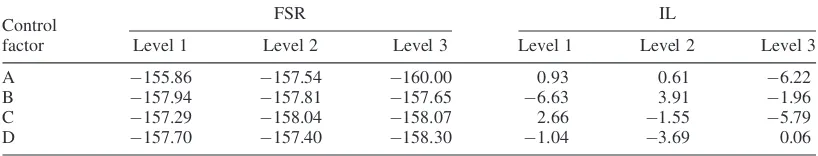
Table 7 indicates the SNR value for both the FSR and IL, whereas Table 8 summarizes the mean SNR values for each control factor. Basically, the larger the SNR value, the better the output performance. From both tables, the following conclusions can be drawn. Control factor A1 which is the ring radii of 6mm, has the most significant effect on the FSR, whereas the control factor of B2 (separation gap of
50 nm), produces the lowest insertion loss.
Figure 5 illustrates the response graph of S/N ratio for each control factors. It can be deduced that to obtain the best FSR value, the optimum combination of control factors and its level is A1, B3, C1, and D2 and for best IL value, the combination should be A1, B2, C1, and D3.
Table III. Noise factors.
Symbol Parameter Unit Level 1 Level 2 Level 3
R Surface roughness nm 0 2 4
S Slope angle 0 5 10
Table II. Experimental layout using orthogonal array.
Exp. no.
Control factor level
A B C D
1 1 1 1 1
2 1 2 2 2
3 1 3 3 3
4 2 1 2 3
5 2 2 3 1
6 2 3 1 2
7 3 1 3 2
8 3 2 1 3
9 3 3 2 1
Table IV. Simulation parameters
Parameter Value
Si refractive index 3.5
SiO2refractive index 1.45
Air refractive index 1.0
Grid size 0.05
Alpha 0
Table VI. Results of L9experiment for insertion loss values of microring resonator channel droppingfilter.
Exp. no.
Insertion loss, dB
R1S1 R1S2 R1S3 R2S1 R2S2 R2S3 R3S1 R3S2 R3S3
1 0.943 0.950 0.957 0.941 0.910 0.946 0.925 0.917 0.915
2 0.596 0.607 0.621 0.614 0.609 0.617 0.619 0.605 0.616
3 1.250 1.342 1.287 1.238 1.279 1.223 1.248 1.217 1.345
4 1.379 1.386 1.388 1.387 1.380 1.383 1.383 1.388 1.393
5 0.854 0.837 0.730 0.725 0.744 0.736 0.742 0.726 0.743
6 0.767 0.773 0.773 0.761 0.763 0.772 0.769 0.762 0.769
7 7.640 7.601 7.645 7.618 7.625 7.595 7.670 7.608 7.646
8 0.563 0.554 0.553 0.558 0.549 0.572 0.553 0.546 0.562
9 2.112 2.151 1.930 1.995 2.039 1.850 2.162 1.881 2.009
Table VII. Signal-to-noise ratio for microring resonator channel dropping wavelengthfilter.
Exp. no.
SNR (dB)
FSR IL
1 155.39 0.59
2 155.71 4.27
3 156.48 2.08
4 158.42 2.83
5 157.72 2.37
6 156.48 2.30
7 160.00 17.65
8 160.00 5.09
9 160.00 6.09
SNR, signal-to-noise ratio; FSR, free spectral range.
Table VIII. Signal-to-noise ratio evaluation for various microring resonator channel droppingfilter performance.
Control factor
FSR IL
Level 1 Level 2 Level 3 Level 1 Level 2 Level 3
A 155.86 157.54 160.00 0.93 0.61 6.22
B 157.94 157.81 157.65 6.63 3.91 1.96
C 157.29 158.04 158.07 2.66 1.55 5.79
D 157.70 157.40 158.30 1.04 3.69 0.06
FSR, free spectral range; IL, insertion loss.
Table V. Results for L9experiments for free spectral range values of microring resonator channel droppingfilter.
Exp. no.
FSR, nm
R1S1 R1S2 R1S3 R2S1 R2S2 R2S3 R3S1 R3S2 R3S3
1 17.0 17.0 17.0 17.0 17.0 17.0 17.0 17.0 17.0
2 16.0 16.0 16.5 16.5 16.5 16.5 16.5 16.5 16.5
3 15.0 15.0 15.0 15.0 15.0 15.0 15.0 15.0 15.0
4 12.0 12.0 12.0 12.0 12.0 12.0 12.0 12.0 12.0
5 13.0 13.0 13.0 13.0 13.0 13.0 13.0 13.0 13.0
6 15.0 15.0 15.0 15.0 15.0 15.0 15.0 15.0 15.0
7 10.0 10.0 10.0 10.0 10.0 10.0 10.0 10.0 10.0
8 10.0 10.0 10.0 10.0 10.0 10.0 10.0 10.0 10.0
9 10.0 10.0 10.0 10.0 10.0 10.0 10.0 10.0 10.0
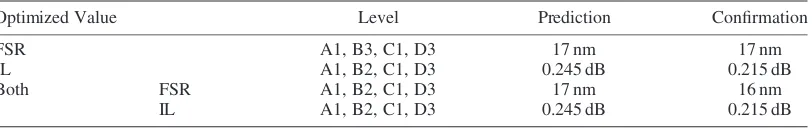
From the parameters shown in Table 9, we canfinally predict the parametric combination to obtain the optimum design trade-off. By comparing the percentage of control factor effects on the device performance, we have selected the control factor combination that exhibits the highest value. The optimized combinations for both FSR and IL is A1, B2, C1, and D3 or wavelengthfilter with 6mm ring
radius with the separation gap of 50 nm and 350 nm350 nm rib waveguide cross-section. This
combination is similar to the optimized combinations for IL.
4.3. Confirmation test
The confirmation test was conducted to verify the results using the predicted control factors and the
final results are shown in Table 10. It confirms that the same FSR is produced as predicted. Meanwhile, the insertion loss improves almost 14% with the new setting. The result proves that thefinal experiment value is correlated with the predicted result with only 1.03 dB error in FSR setting and 0.08 dB error for IL. In the meantime, to find the trade-off between both outputs, a confirmation test was once again performed with the parametric combination selected before. Thereupon, the IL value is identical and
the FSR lessen. Thefinal device with control/noise factors of A1B2C1D3R3S2 gives an FSR value
of 16 nm and IL of 0.215 dB.
S/N Ratio (dB) S/N Ratio (dB)
Control Factor Levels
Figure 5. S/N ratio for (a) free spectral range (b) insertion loss.
Table IX. Optimum parametric combination for free spectral range and insertion loss and percentage of effect.
Control factor
FSR IL
Level % Factor effect Level % Factor effect
A 1 91 1 26
B 3 0 2 41
C 1 4 1 27
D 3 4 3 6
FSR, free spectral range; IL, insertion loss.
Table X. Predicted and confirmation results of L9experiment.
Optimized Value Level Prediction Confirmation
FSR A1, B3, C1, D3 17 nm 17 nm
IL A1, B2, C1, D3 0.245 dB 0.215 dB
Both FSR A1, B2, C1, D3 17 nm 16 nm
5. CONCLUSIONS
We have presented an analysis and optimization of wavelength filter design using the Taguchi
method. From this work, it is proven that choosing the appropriate design parameters is crucial in
designing an optimum MRR channel dropping filter. We found that the ring radius has the most
significant effect on FSR performance, whereas the separation gap has the largest effect on the IL. It also proven that the Taguchi method can be successfully applied to predict the optimum solutions
in designing an MRR channel dropping filter. The final device with control/noise factors of
A1B2C1D3R3S2 gives an FSR value of 16 nm and IL of 0.215 dB. This parametric combination will be utilized in the actual fabrication process. Hence, Taguchi optimization prior to fabrication provides a methodology with reduced cost and time as well provides insight into the effect of design factors on output characteristics.
ACKNOWLEDGEMENT
The authors would like to acknowledge Prof P.R. Apte (IIT Bombay) for their input on the Taguchi method. The authors would also like to thank the Universiti Teknikal Malaysia Melaka (UTeM) and the Ministry of Higher Education for the support. This research is supported by a funding from the Universiti Kebangsaan Malaysia, grant no: UKM-OUP-NBT-27-118/2012.
REFERENCES
1. Rabiei P, Steier WH, Zhang C, Dalton LR. Polymer micro-ring
filters and modulators.J Lightwave Technol2002;20(11):1968–1975. 2. Haroon H, Shaari S, Menon PS,
Mardiana B, Abdul Razak H, Arsad N, Majlis BY, Mukhtar WM, Abdullah H. Design and characteri-zation of multiple coupled microring based wavelength demultiplexer in silicon–on–insulator (SOI). J Nonlinear Opt Phys Mater 2012;
21(1):1250004-1-8.
3. Chao CY, Fung W, Guo LJ. Polymer microring resonators for biochemical sensing applications.
Opt Express2010;18(2):393–400. 4. Shaari S, Hanim AR, Mardiana B, Hazura H, Menon PS. Modeling and analysis of lateral doping region translation variation on optical
mod-ulator performance,in the 4th Asian Physics Symposium AIP Confer-ence Proceedings1325(September 2010), pp. 297–300.
5. Van V. Synthesis of elliptic optical
filters using mutually coupled microring resonators. J Lightwave Technol2007;25(2):584–590. 6. Xioa S, Khan MH, Shen H, Qi M.
Silicon-on-insulator microring add-dropfilters with free spectral range over 30nm. J Lightwave Technol
2008;26:297–2010.
7. Yang P, Tan G. Taguchi-numerical approach on thermomechanical reliability for PBGA.Int J Numer Modell: Electron Networks, Devices Field2011;24(5):437–447. 8. Elgomati HA, Majlis BY, Ahmad I,
Salehuddin F, Hamid FA, Zaharim A, Apte PR. Application of Taguchi method in the optimization of process variation for 32nm CMOS
technology. Aust J Basic Appl Sci
2011;5(7):346–355.
9. Haroon H, Abdul Razak H, Bidin M, Shaari S, Menon PS. Free carrier absorption loss of p-i-n silicon-on-insulator (SOI) phase modulator. International conference on en-abling science and nanotechnology (Escinano) 2010 AIP Conference Proceedings;1341, 241–244. 10. Shaari S, Hanim AR, Mardiana B,
Hazura H, Menon, PS. Modeling
Sahbudin Shaari received his BSc degree in Physics from the Universiti Kebangsaan Malaysia (UKM), MSc degree in Quantum Electronics from the Uni-versity of Essex, UK, and PhD degree in Microelectronics from the UniUni-versity of Wales, UK in 1978, 1980, and 1989, respectively. He joined the UKM in 1978 as an academic staff and later was promoted to associate professor in 1992. Currently, he is a professor and principal research fellow at the Institute of Microenginering and Nanoelectronics (IMEN), UKM since 2002. His current research interests include PLC and SOI photonic devices, photo-detectors and semiconductor lasers, optical CDMA and CWDM-PON. He is also a member of IEEE since 1986, Prof Shaari is also a member of the International Society for Optical Engineering (SPIE), mem-ber of the Optical Society of America (OSA), and a memmem-ber of the Malaysia Solid State Science Society (MSSS). He was a conference chairman, technical chairman, and member of the organizing committee for the IEEE International Conference on Semiconductor Electronics since 1992 until 2011.
P Susthitha Menoncompleted her BEng (Hons) degree at the Universiti Kebangsaan Malaysia (UKM), Bangi, Malaysia specializing in Electric, Electronics, and System Engineering in 1998. After that, she worked at the Intel Products Malaysia Pte. Ltd. until 2002 as a product engineer for mobile modules and motherboard systems until 2002. In 2005, she completed her MSc degree specializing in Microelectronics at UKM where she developed a silicon lateral p-i-n photodiode (LPP). Later, in 2008, she completed her PhD degree with Distinction at the Institute of Micro-Engineering & Nanoelectronics (IMEN), UKM where she developed an InGaAs-based interdigi-tated lateral p-i-n photodiode (ILPP). She joined IMEN, UKM as a postdoctoral fellow in 2008 and worked on the development of GaAs/InP-based LW-VCSELs. Since 2009, she is a research fellow at IMEN, UKM specializing in thefield of optoelectron-ics, nanophotonoptoelectron-ics, III-V materials, optical communications, and statistical optimiza-tion. P Susthitha Menon is currently the secretary of the IEEE Electron Devices Malaysia Chapter, member of the International Society for Optical Engineering (SPIE) and member of the Optical Society of America (OSA). To date, she has authored/co-authored more than 50 Scopus-indexed international journal and proceedings. She can be contacted at [email protected].
Hanim Abdul Razak was born in Melaka, in 1979. She received his Bachelor degree in Computer and Information Engineering from the International Islamic University Malaysia in 2003. Later, she completed her MSc degree in Microelec-tronics from the Universiti Kebangsaan Malaysia in 2006. Since 2003, she has been with the Universiti Teknikal Malaysia Melaka as a lecturer. Currently, she is pursu-ing her PhD degree at the Institute of Microengineerpursu-ing and Nanoelectronics (IMEN), Universiti Kebangsaan Malaysia. Her area of research includes silicon photonics, focusing on the Mach Zehnder Modulator.