LOW NOISE AMPLIFIER AT 2.4GHZ FOR WLAN APPLICATION
SITI ADLINA BTE MD ALI
UNIVERSITI TEKNIKAL MALAYSIA MELAKA
SITI ADLINA BTE MD ALI
This report is submitted in partial fulfillment of requirements for the Degree of Bachelor in Electrical Engineering (Telecommunication Electronics)
Faculty of Electronic and Computer Enginnering Universiti Teknikal Malaysia Melaka
“I hereby declare that this report is the result of my own work except for quotes as citied in the references.”
Signature :………
Author : SITI ADLINA BTE MD ALI
“I hereby declare that I have read this report and in my opinion this report is sufficient in terms of the scope and quality for the award of Bachelor of Electronic Engineering
(Telecommunication Electronics) with honors.”
Signature :………
Supervisor’s Name : MR. ZOINOL ABIDIN BIN ABD AZIZ
ACKNOWLEDGEMENT
Praise the lord the Almighty One for giving me the patience, wisdom and perseverance to complete this project. I would like to take this opportunity to express my gratitude to my supervisor, Mr. Zoinol Abidin Bin Abd Aziz for his patience and guidance in helping me to complete this project.
My special thanks to Mohd Hafizan Che Halim (master student) for his kind suggestions and help during the work. I also thank to the entire BENT 08/09 final years student’s at UTEM who made this thesis work easy and fast.
ABSTRACT
ABSTRAK
TABLE OF CONTENTS
CHAPTER TITLE PAGE
DECLARATION DEDICATION
ACKNOWLEDGEMENTS ABSTRACT
ABSTRAK
TABLE OF CONTENTS LIST OF TABLES LIST OF FIGURES
LIST OF ABBREVIATION LIST OF APPENDICES
ii iii iv v vi vii ix x xii xiv
1 INTRODUCTION
1.1 Introduction 1.2 Problem Statement 1.3 Objective
1.4 Scope of Project 1.5 Methodology 1 1 3 4 5 6
2 BACKGROUND STUDY
2.1 WLAN Basic 2.2 Standard of WLAN
2.3 Single Stage Transistor Amplifier Design 2.4 Characteristics of Microwave Transistor
7 7 8 10 12
3 THEORY
3.1 Introduction 3.2 DC Biasing
3.3 Stability of Amplifier
3.4 Input and Output Matching
3.4.1 Quarter Wave Transformer matching 3.4.2 Single Stub matching
3.5 Planar Transmission Lines 3.5.1 Strip Line
3.5.2 Micro-strip 3.6 Two Port Power Gain
3.6.1.0 Single Stage Transistor Amplifier Design
3.6.1.1 Design for Maximum Gain 3.6.1.2 Low Noise Amplifier Design
3.6.1.2 Constant Gain Circle and Design for Specified Gain
3.6.2.0 Broadband Amplifier Design
3.6.2.1Balanced Amplifier 3.6.2.2 Distributed Amplifier
24 26 28 31 31 32 33 37 38 42 43 45 47 49 4 5
DESIGN LOW NOISE AMPLIFIER 4.1 Transistor Selection
4.2 Project Methodology 4.2.1 Flow Chart
4.2.2 Explanation of Flow Chart 4.3 Transistor Biasing
4.4 Transistor Stability 4.5 Design Process
4.6 Input and Output Matching
RESULT AND DISCUSSION 5.1 Requirements
5.2 Simulation Result
5.2.1 Design for Maximum Gain 5.2.2 Low Noise Amplifier Design
6
5.3 Theory and Simulation Comparison
5.3.1 Input and Output Matching Comparison 5.3.2 Gain and Noise Comparison
CONCLUSIONS
6.1 Discussion and Conclusions 6.2 Future Work
REFERENCE APPENDICES
70 71
71 72
\
LIST OF TABLE
TABLE TITLE PAGE
1 2 3 4 5 6 7 8 9 10 11
WLAN IEEE 802.11 Standards
Summarizes of Stability Factor at 2.4GHz ATF 54143 Biasing
Gain, Center And Radius Of Input Constant Gain Circle Gain, Center And Radius Of Input Constant Gain Circle Gain, Center And Radius Of Output Constant Gain Circle
Width and Length of Input and Output Impedance Width and Length of Input and Output Impedance Width and Length of Input and Output Impedance Port Matching Comparison
Designs for Maximum Gain Low Noise Amplifier Design
Constant Gain Circle and Design for Specified Gain
LIST OF FIGURES
FIGURE TITLE PAGE
1 2 3 4 5 6 7 8 9 10 11 12 13 14 15 16 17
Low Noise Amplifier signal Project Methodology Amplifier Classes
The cross section, top view and equivalent circuit of transistors GaAs FETs and Silicon Bipolar
Five Basic Dc Bias Networks Input Stability Circle
Output Stability Circle
Matching With a Single Section Quarter-Wave Transformer
The Quarter-Wave Transformer Solution Single Stub Tuning Circuit
The Single Stub Matching Solution Strip-line Transmission Line Micro-strip transmission line
A Two-Port Networks With General Source and Load Impedances
The General Transistor Amplifier Circuit
A Balanced Amplifier Using 900 Hybrid Couplers Configuration Of An N Stage Distributed Amplifier
18
19 20 21 22 23 24 25 26 27
General Flow Chart of Designing Low Noise Amplifier ATF 54143 Biasing Circuit
S Parameters of Maximum Gain Amplifier Noise Figure
Noise
S Parameters of Low Noise Amplifier Noise Figure
Noise
S Parameters of Specified Gain Amplifier Noise Figure
Noise
LIST OF APPENDICES
INDEX
A B C D E F G
TITLE
Data Sheet of ATF 54143 Stability Circle
Low Noise Amplifier Design
Constant Gain circle and Design for Specified Gain Maximum Gain Design Matching
Low Noise Amplifier Design Matching
Constant Gain circle and design for Specified Gain Matching
PAGE
CHAPTER 1
INTRODUCTION
1.1 Introduction
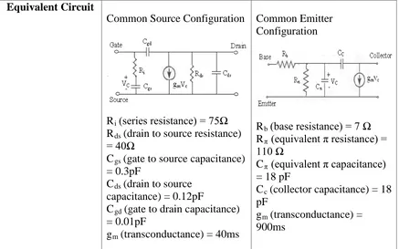
Over recent years, the interest in microwave techniques for communication systems has grown tremendously and also the development and the performance of microwave active and passive circuits for wireless technologies has become extremely advanced. Microwave amplifiers have become one of the most critical active circuits that employed in the system applications, [1]. Low Noise Amplifies (LNA’s) are found in many applications, especially, LNA’s are used to amplify the received low power signal and separate it from the noise floor, [2]
(a) (b)
Figure 1 Low Noise Amplifier signal a) Input of LNA b) Output of LNA
1.2 Problem Statement
In general, received signals at receiver of Wireless LAN antenna contain noise. The medium between transmitter and receiver of Wireless LAN antenna is air, so the possibility of having noise is high. The noises are due to attenuation, interference, crosstalk and power adjacent. Transmission line also contributes to produce noise in the signal. So, received signals at receiver’s antenna will have usable signal adding by noise which cannot be differentiate.
1.3 Objectives
The objectives of this Low Noise Amplifier design are to design and simulate Low Noise Amplifier circuit for WLAN application. The design, simulate and measure steps will considers stability, gain and noise figure parameters. While the design process will be done by calculates related parameters by using ideal microwave amplifier equations.
1.4 Scope of Work
The scope of work for this project can be divided into four parts which are:
• The first part is designing Low Noise Amplifier by using ATF 54143 – It involves selection of proper transistor, checking the transistor stability and calculates the gain and noise figure parameters by using maximum gain method. All the parameters will be calculated by using ideal microwave amplifier equations.
• The second part is simulation by using Advanced Design System (ADS2006) to make sure the results are close to the calculated design parameters.
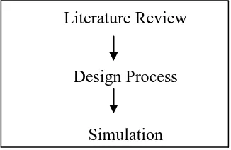
1.5 Methodology
The first step of this project is review the background of designing Low Noise Amplifier and the application in Wireless LAN system. Reviewing of LNA done by find all journals, articles, books, and website which are related. Most of the journals and articles are referring to Institute of Electrical and
Electronics Engineers (IEEE) website.
Then, the second step is design process which done by calculate stability, gain and noise figure of the ATF 54143 transistor at 2.4 GHz by using maximum gain method. The parameters calculation will refer to ideal microwave amplifier equations.
The third step is simulation process that done by using Advance Design System (ADS). Before start the simulation, the study of the ADS software is done. The simulation will consider stability, gain and noise figure of the ATF 54143 transistor at 2.4 GHz. All the simulation parameters will more less same to calculated parameters.
All the third steps will be used to design Single Stage Low Noise Amplifier with three different methods which are Design for Maximum Gain, Low Noise Amplifier Design and Design for Specified Gain
Literature Review
Design Process
[image:19.612.239.402.584.690.2]Simulation
CHAPTER 2
BACKGROUND STUDY
2.1 Introduction to WLAN Basics
New communication systems operate in the frequency range 1-100 GHz;
third generation mobile phone telephony utilizes the frequency band 1.9-2.2
GHz, wireless local area networks (WLAN’s) operate at the frequency band
2.4-5 GHz and automobile radar system work at 77 GHz. WLAN’s data
communication systems are implemented as an alternative to wired local area. It is the most convenient way to establish high speed Internet and Internet connections and distributes data throughout the area.
.
A Wireless LAN (WLAN) is Wireless Local Area Network which links
two or more devices by using Spread Spectrum or Orthogonal Frequency
Division Multiplexing (OFDM). This enables communications between devices
in a limited area. Users can move around within a broad coverage area and still
be connected to the network. The advantages of WLAN are easy installation and
2.2 Standard of WLAN
[image:21.612.151.539.383.553.2]The market of Wireless Local Area network (WLAN) is in constant explosion since its appearance in the 90’s. The constant demand on increased speed has pushed the early 802.11 standard. It is also known as WiFi with 2 Mb/s data rate to move 802.11b standard with 11 Mb/s data rate and finally to the 802.11g which reaches 54 Mb/s data rate. Both 802.11b and 802.11g standards are operates at 2.4 GHz. IEEE 802.11 is family of wireless standards [4].
Table 1 WLAN IEEE 802.11 Standard [5]
Protocol 802.11a 802.11b 802.11g
Release Date 1999 1999 2003
Frequency (GHz) 5.15-5.35 5.47-5.725 5.725-5.875
2.4-2.5 2.4-2.5
Max Bandwidth (Mbps) 54 11 54
Range Indoor (m) 25 35 25
Range Outdoor (m) 75 100 75
802.11b works on the frequency of 2.4 GHz with maximum bandwidth
of 11 Mbps. 802.11b uses DSSS (Direct-sequence spread spectrum) and CCK
(Complementary Code Keying) on the frequency 2.4 to 2.483 GHZ. DSSS is the
modulation technique in which transmitted signal takes up more bandwidth than
the information signal that is being modulated. Its range in the indoor
802.11g was released in June 2003. It works on frequency of 2.4 GHz,
but its maximum bandwidth is 54 Mbps. 802.11g uses Orthogonal
Frequency-Division Multiplexing (OFDM) for 54, 48, 36, 24, 18, 12, 9, 6 Mbps. For 11 and
5.5 Mbps it uses CCK and DSSS (like 802.11b). Its range in the indoor
environment is about 25 meters and 75 meters in outdoor environment.
2.3 Characteristics of Microwave Transistors
Microwave transistors are used as amplifiers, oscillators, switches, phase shifters, mixers and active filters. Most of these applications used either silicon bipolar transistors or GaAs field effect transistors (FETs). Silicon bipolar device technology is very mature and inexpensive compared to GaAs transistor technology. Bipolar transistors are capable of higher gain and power capacity at lower frequencies, but GaAs FETs generally have better noise figures and can operate at much higher frequencies.
Microwave Field Effect transistors can be used at frequencies well into the millimeter wave range with high gain and low noise figure, making them the device of choice for hybrid and monolothic integrated circuits at frequencies above 5 to 10 GHz [5]. In order to operate the transistor, positive Vds is supply to drain port. An input signal voltage on the gate then modulates
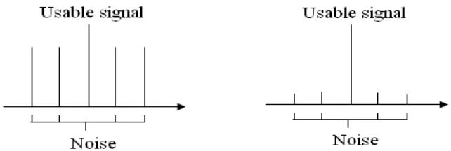
Microwave bipolar transistors are usually of the NPN type and are often preferred over GaAs FETs at frequencies below 2 to 4 GHz because of the higher gain and lower cost [5]. Noise figure of bipolar transistors is not good as FETs because bipolar transistors are subject to shot noise as well as thermal noise effects. Figure 3 summarizes the cross section, top view and equivalent circuit of transistors GaAs FETs and Silicon Bipolar.
Transistor GaAs FET Silicon Bipolar Transistor Cross
Section of Transistor
Equivalent Circuit
Common Source Configuration
Ri (series resistance) = 75Ω Rds (drain to source resistance) = 40Ω
Cgs (gate to source capacitance) = 0.3pF
Cds (drain to source capacitance) = 0.12pF
Cgd (gate to drain capacitance) = 0.01pF
gm (transconductance) = 40ms
Common Emitter Configuration
Rb (base resistance) = 7 Ω Rπ (equivalent π resistance) = 110 Ω
Cπ (equivalent π capacitance)
= 18 pF
Cc (collector capacitance) = 18 pF
[image:24.612.111.548.141.414.2]gm (transconductance) = 900ms
Figure 3 The cross section, top view and equivalent circuit of transistors GaAs FETs and Silicon Bipolar. [5]
2.4 Single Stage Transistor Amplifier
![Table 1 WLAN IEEE 802.11 Standard [5]](https://thumb-ap.123doks.com/thumbv2/123dok/643274.78264/21.612.151.539.383.553/table-wlan-ieee-standard.webp)