Volume 2010, Article ID 923409,8pages doi:10.1155/2010/923409
Research Article
Growth of AlGaSb Compound Semiconductors on GaAs Substrate
by Metalorganic Chemical Vapour Deposition
A. H. Ramelan,
1H. Harjana,
1and P. Arifin
21Physics Department, Research Centre for Smart Materials and Energy, Faculty of Mathematics and Natural Sciences (FMIPA),
Sebelas Maret University (UNS), Jl. Ir. Sutami no. 36A, Surakarta 57126, Indonesia
2Physics Department, Electronic Materials Laboratory, Faculty of Mathematics and Natural Sciences (FMIPA),
Bandung Institute of Technology (ITB), Jl. Ganesha no. 10, Bandung 40132, Indonesia
Correspondence should be addressed to A. H. Ramelan,aramelan [email protected]
Received 14 August 2010; Accepted 1 October 2010
Academic Editor: Maria Antonietta Loi
Copyright © 2010 A. H. Ramelan et al. This is an open access article distributed under the Creative Commons Attribution License, which permits unrestricted use, distribution, and reproduction in any medium, provided the original work is properly cited.
Epitaxial AlxGa1-xSb layers on GaAs substrate have been grown by atmospheric pressure metalorganic chemical vapour deposition using TMAl, TMGa, and TMSb. We report the effect of V/III flux ratio and growth temperature on growth rate, surface morphology, electrical properties, and composition analysis. A growth rate activation energy of 0.73 eV was found. For layers grown on GaAs at 580◦C and 600◦C with a V/III ratio of 3 a high quality surface morphology is typical, with a mirror-like
surface and good composition control. It was found that a suitable growth temperature and V/III flux ratio was beneficial for producing good AlGaSb layers. Undoped AlGaSb grown at 580◦C with a V/III flux ratio of 3 at the rate of 3.5µm/hour shows
p-type conductivity with smooth surface morphology and its hole mobility and carrier concentration are equal to 237 cm2/V.s and 4.6×1017cm-3, respectively, at 77 K. The net hole concentration of unintentionally doped AlGaSb was found to be significantly decreased with the increased of aluminium concentration. All samples investigated show oxide layers (Al2O3, Sb2O3, and Ga2O5) on their surfaces. In particular the percentage of aluminium-oxide was very high compared with a small percentage of AlSb. Carbon content on the surface was also very high.
1. Introduction
Because of the corresponding wavelengths of the alloys of gallium antimonide- (GaSb-) based compound semicon-ductors cover a wide spectral range from 1.24µm (AlGaSb or AlGaAsSb) to 4.3µm (InGaAsSb), they have received increasing attention recently. Consequently, they became promising candidates for applications in long wavelength lasers and photodetectors for fibre optic communication systems [1–3].
It is ideal to grow the AlGaSb films on lattice-matched GaSb substrates. However, due to the lack of semi-insulating GaSb, undoped substrates have a strong free carrier absorp-tion in the mid-IR wavelength region of interest, so that the substrate must be thinned for optimal device operation in the flip-chip mode. For this and commercial reasons, GaAs has been explored as a substrate for GaSb/AlGaSb devices. Unfortunately, a lattice mismatch of approximately 7% exists
between GaSb and GaAs. Strain energy can be accommo-dated by misfit dislocations at the GaAs/GaSb interface. This results in the propagation of threading dislocations through the epilayers [4]. Thus, the growth of undoped high-quality GaSb/AlGaSb layers on GaAs substrate becomes a necessary process for preparing thin layers.
major reasons: the vapour pressure of antimony over the growing surface, the lack of a stable group V hydride, the kinetically controlled nature of the growth, and the lack of an insulating antimonide substrate.
In this work, a series of undoped AlGaSb samples were grown on semi-insulating GaAs substrates by MOCVD technique. The growth rates, surface morphology and elec-trical properties of AlGaSb were studied as functions of growth temperatures and V/III flux ratio. The elemental microanalysis was also investigated.
2. Experimental Procedure
2.1. Growth Conditions. The growth was carried out in a
horizontal MOCVD reactor at atmospheric pressure. The precursors were trimethylaluminum (TMAl), trimethylgal-lium (TMGa), and trimethylantimony (TMSb) held at a temperature of 18◦C, −9◦C and 0◦C, respectively. Source materials were diluted in hydrogen to obtain a carrier gas velocity of 1 sccm in the reactor. The substrate was (100) oriented semi-insulating GaAs. GaAs substrates were prepared by degreasing in trichloroethylene (TCE), rinsing in acetone and methanol. The GaAs substrate was etched in a standard solution of H2SO4, H2O2, and H2O (5 : 1 : 1) for
30 s [11]. The substrates were further rinsed in DI water and rapidly dried under a nitrogen jet.
To minimize oxidation, the substrates were transferred immediately after preparation into a glove box having nitrogen ambient from which they were loaded into the reactor. Before the growth the reactor was evacuated and refilled with hydrogen several times. The GaAs substrate was baked under TMSb partial pressure at a temperature of 640◦C for 15 minutes to remove the residual oxide film. The growths were performed at temperatures of 580◦C and 600◦C measured by a thermocouple located inside the graphite susceptor. The actual temperature of the substrate surface is assumed to be lower due to the cooling effect of the cold carrier gas.
2.2. Characterisation. The surface morphologies of the
grown epilayers were observed using Nomarski contrast microscopy. Thicknesses were measured using a Tencor Alpha Step 500 surface profiler. A stylus profiler was routinely employed to record the surface profile of etched AlGaSb samples. The AlGaSb samples deposited on semi-insulating GaAs substrates were characterized by making Van der Pauw structures. Ohmic contacts were formed on the four corners of the square sample using TiAu and/or indium contacts annealed under a nitrogen flow at 250◦C. A CTI closed cycle refrigerator (Model 22C/350C) was used for Hall measurement for the temperature range of 10 K–300 K. A VG ESCALAB 220i-XL Analytical XPS system was employed to determine the presence of elements in the samples. Monochromatic AlKα (1486.6 eV) X-rays flood the sample, the generated photoelectrons are detected by a multidetector concentric hemispherical analyzer (CHA).
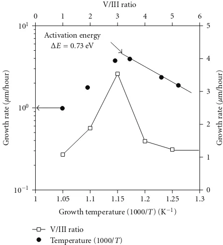
Figure 1: Temperature dependence of the Al0.05Ga0.95Sb growth
rates and the growth rate of Al0.05Ga0.95Sb epilayers grown at 580◦C as a function of V/III ratio.
3. Results and Discussion
3.1. Growth Rate. The two growth parameters that most
strongly affect the growth rates are the metalorganic sources partial pressure and the growth temperature. Growth rate is defined as the thickness of the epilayer deposited on a substrate during a certain period of growth. The effect of growth temperature, in the range 520◦C–680◦C, on the growth rate was investigated by keeping thers parameters constant. Constant flow rates of TMAl=5.6 sccm, TMGa=
19.1 sccm, and TMSb=83.6 sccm, or equivalent to V/III=3
were used.
Figure 1 shows the temperature dependence of growth rates for Al0.05Ga0.95Sb. In the low temperatures range up
to 540◦C, kinetic processes of alkyl decomposition at the substrate surface limit decomposition. This is known as the kinetically controlled regime, where the growth rate depends on temperature (degree of pyrolysis) and very little dependence of growth rate on pressure was observed. A typical exponential relationship between growth rate and growth temperature was observed and the activation energy of 0.73 eV was found. Ungermanns et al. [12] have found an activation energy of 0.80 eV for AlSb growth using dimethylethylaminealane (DMEAAl) as the aluminium source.
of the low vapour pressure. Since Ga and Al atoms tend to desorb from the excessively Sb absorbed surface, only a few Ga and Al species can contribute to the growth. This is known as the site-blocking effect. Therefore, a higher growth rate, for Sb-containing alloys, will be obtained for lower Sb surface coverage condition by selecting higher growth temperatures and/or lower V/III ratio. However, the low surface coverage of Sb may lead to the formation of Ga droplets. For higher temperatures, in the range of 580◦C to 600◦C the growth rate is constant. This region is a mass transport limited (i.e., the growth rate is controlled predominantly by the concentration of the precursors), because of the complete pyrolysis of the TMGa and TMSb molecules. Further increase in the growth temperatures, leads to a decrease of the growth rate due to desorption of gallium and antimony from the growth surface. The growth rate is not only a function of the availability of atomic species and the rate at which the precursor fragments combine at the surface, but also depends on the carrier gas velocity and the partial pressure of the metalorganic sources [14].
The V/III ratio is another key parameter because both a deficiency and excess of antimony (Sb) on the semiconductor surface lead to a strong degradation of the material quality.
Figure 1 shows also the growth rate for the Al0.05Ga0.95Sb
films as a function of the V/III ratio. The data indicate that the growth rate is significantly dependent on V/III ratios. At V/III ratios below about 2, the growth rate is low, under 1.87µm/hour. As the V/III ratio increases, the growth rate increases to reach value of 3.54µm/min near a V/III ratio of 3. In this region, the availability of Sb appears to be the key factor controlling the growth rate. At higher V/III ratios, the growth rate starts to decrease. The strong decrease of the growth rate with increasing TMSb (group V) is caused by excess antimony molecules (due to the low vapour pressure of TMSb) at the substrate surface which leads to a decrease to the number of surface sites available for Al and Ga adsorptions and a resulting absolute decrease in Al and Ga adatoms. This blocking of Al and Ga adatoms by excess Sb results in reduced growth rates. Similar behaviour was reported by Okuno et al. [15] for AlGaSb growth using TMAAl (trimethylaminealane), TMGa and TMSb.
The influence of the alloy composition on the growth rate of AlxGa1−xSb epilayers was also investigated while
keeping the other growth parameters (i.e., temperature, V/III ratio) constant. The result shows the growth rate as a function of alloy composition for two sequences of the AlxGa1−xSb epilayers grown at 580◦C and 600◦C. The growth
rate does not change significantly over the range of alloy compositions investigated. With respect to good surface morphology and high growth rate, the optimum V/III ratios of 3 for AlxGa1−xSb (15≤X≤20) in the growth temperature
range from 580◦C to 600◦C have been determined.
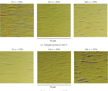
3.2. Surface Morphology. Figure 2 shows the surface
mor-phology of selected AlxGa1−xSb compositions for V/III ratio = 3 at 580◦C and 600◦C, respectively. The morphology
of AlxGa1−xSb on GaAs is mirror-like to the naked eye,
but the epilayers exhibit microscopic well-defined elongated
features. As the Al content increases, the surface texture changes and the elongated features disappear, to be replaced by featureless texture associated with the highest optical transmission. The interference fringe modulation depths of the epilayers obtained from transmission measurements confirm the high optical quality of the films grown at 580◦C. With further increase of Al content, several vessel-shaped structures appear on the epilayer surface. It has been found for this project that the AlxGa1−xSb layers grown
at 580◦C and 600◦C and V/III
= 3 with Al composition
in the range of 0.5% and 30% are highly regular and accompanied by excellent optical quality, with a very high optical transmission at energies below the bandgap.
3.3. Electrical Properties. For electrical characterisation of the
GaSb/AlGaSb layers, semi-insulating GaAs substrates (with lattice mismatch ∆a/a around 7.5%) were used because SI GaSb substrates are not available commercially. The dislocations created by this lattice-mismatch are expected to propagate through the AlGaSb epilayer, as previously shown for GaInAsSb epilayers grown on SI-GaAs with an 8% lattice mismatch [16]. However, for our lattice-mismatched layers, the layer thickness may influence the electrical properties, this is due to the reduction of dislocation density with sufficiently thick layers. In fact, Pascal et al. [17] reported that the mobility values for GaSb layers grown on GaAs are only slightly lower than in bulk samples indicating a small influence of the dislocations on the carrier diffusion process. In addition, the variation of the lattice constant for the AlxGa1−xSb being investigated is relatively small
(∆a/a = 0.65% for GaSb/AlSb). Therefore, the electrical
measurement of the AlxGa1−xSb epilayer growns on SI-GaAs
may also be relatively unaffected by the lattice mismatch. Unintentionally undoped AlGaSb is always p-type. The origin of p-type conduction of AlGaSb alloys was often attributed to native lattice defects (i.e., Sb vacancies), antisite defects (Ga atoms in Sb sites), and complex defects (VGaGaSb) [18, 19]. Another possible explanation for
p-type conduction might be that carbon atoms occupy group-V element sites as acceptor in the materials, as shown
by MOVPE-GaAs [20]. The strong Ga-C bond forces
carbon onto the group-V sublattice, and therefore carbon is an acceptor. In our studies, we achieved for undoped Al0.1Ga0.9Sb layers (thickness ∼3.5µm) grown under
opti-mum growth conditions, hole concentrations of 4.6 × 1017cm−3 (77 K), and mobilities of 237 cm2/V.s (77 K).
Meanwhile, the Al0.1Ga0.9Sb layer grown by Chidley et al.
[21] with the same metalorganic sources with our system has a hole concentration of 5×1017cm−3(77 K) and mobilities of 232 cm2/V.s (77 K). As shown inTable 1, the comparison
of the hole concentration and mobility in AlxGa1−xSb grown
by other groups. Therefore, the electrical quality of our AlGaSb layers is comparable to the best data AlGaSb films grown by other atmospheric pressure MOVPE. The undoped GaSb/AlGaSb with a thickness in the range of 2.3µm–5.6µm has been grown as well in our MOCVD system, and the hole concentration in the range of 1016–1019cm−3 were
50µm
(ii)x=20% (iii)x=25%
(i)x=10%
(a) Samples grown at 580◦C
50µm
(i)x=15% (ii)x=20% (iii)x=25%
(b) Samples grown at 600◦C
Figure2: Surface morphology of AlxGa1
−xSb epilayers grown on GaAs with a different Alcontent grown at 580◦C and 600◦C with a V/III ratio of 3.
Table1: Hole mobility and carrier concentration of AlxGa1−xSb.
Material Tg (◦C) V/III ratio Mobility (cm2/V.s) Concentration (cm−3) Source
Al0.22Ga0.78Sb 600 2.0 197 (300 K) 1.6×10¹⁸ Koljonen et al. [10]
Al0.32Ga0.68Sb 650 2.5 163 (300 K) 5.7×10¹⁸ Koljonen et al. [10]
Al0.76Ga0.24Sb 650 1.5 93 (300 K) 1.2×10¹⁹ Koljonen et al. [10]
Al0.1Ga0.9Sb 600 — 232 (77 K) 5×10¹⁷ Chidley et al. [21]
Al0.2Ga0.8Sb 600 — 97 (300 K) 5×10¹⁹ Chidley et al. [21]
Al0.1Ga0.9Sb 600 3 237 (77 K) 4.6×10¹⁷ This work
Al0.2Ga0.8Sb 600 3 176 (300 K) 4.0×10¹⁸ This work
Al0.2Ga0.8Sb 580 3 199 (300 K) 2.1×10¹⁸ This work
due to carbon and oxygen incorporation into the layers from the TMAl source.
To investigate the effect of growth temperature on the concentration and mobility, the growth was carried out at temperatures in the range between 520◦C and 680◦C, keeping TMAl, TMGa, and TMSb constant. As shown in
Figure 3, the carrier concentration increases as the growth temperature is increased in the higher growth temperatures from 600◦C up to 680◦C. However, the rapid increase of carrier concentration in the layer grown at 680◦C may be partially attributed to the increase in the defect density in the layer, since we also observed the surface degradation of the layer at this temperature. The increased carrier concentration with the growth temperature could also have been caused
by increased Sb vacancies or perhaps by high antisite defect concentrations. Figure 3 shows also the rapid drop in the mobility at this temperature which supports this conclusion. Similar reason in the low temperature region (below 580◦C), the carrier concentration increases and simultaneously the mobility declines as the growth temperature decreases. The surface layers degradate as the growth temperatures move away below 580◦C. The surface was covered with antimonide precipitates due to incomplete decomposition of the TMSb. Again, the surface degradation is responsible for decreasing the mobility and increasing the carrier concentration.
Growth temperature (◦C)
520 560 600 640 680
1017
Figure3: Dependence mobility and carrier concentration at 300 K
on the growth temperature for Al0.1Ga0.9Sb layers grown on GaAs substrates with a V/III ratio of 3.
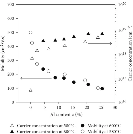
Al-contentx(%)
Carrier concentration at 580◦C
Carrier concentration at 600◦C
M
Figure 4: Mobilities and carrier concentration (300 K) for
AlxGa1−xSb layers grown at 580◦C and 600◦C as a function of Al-content (mol-% AlSb).
When Al is incorporated into GaSb in small quantities of 0 < x < 0.025, the mobility decreases and the carrier concentration increases sharply. Since the GaSb antisite defect is presumed responsible for the acceptors in GaSb, it is suggested that Al more readily occupies VSb sites and
the incorporation of carbon is enhanced by introducing Al into GaSb growth, this increases the acceptor concentration.
Binding energy (eV)
A similar sharp increase of carrier concentration by the incorporation of even a small amount of aluminium had been previously reported by Chidley et al. [21] and is attributed to carbon contamination in the MOCVD growth. The RT mobilities for the growth temperature of 580◦C and 600◦C are very similar, but the carrier concentration is higher for layers grown at 600◦C.
3.4. Elemental Microanalysis. Two main problems in the
application of metalorganic Al sources have been identified. Firstly, the aluminum-carbon bond in the precursor is very stable leading to an increase carbon contamination. Secondly, because of the high affinity of aluminum to oxygen, metalorganic organic aluminium sources react with O2and
form partially oxidized compounds, which often have a higher vapour pressure than their nonoxidized counterparts. Oxygen then incorporates into the material where it tends to form a deep level impurity in such compounds as AlGaSb [11]. Certainly, this unintentional impurity incorporation has a negative influence on the electrical and optical properties of the material. The O and C contents in our MOCVD-grown films were examined.
Figure 5is an XPS wide scan spectrum of Al0.05Ga0.95Sb
Binding energy (eV)
Figure7: XPS narrow scan of Ga3d at the as-received surface of
Al0.05Ga0.95Sb grown at 600◦C with a V/III ratio of 3.
Figure 6shows XPS narrow scan spectra of the Sb3d3/2
and Sb3d5/2peaks at the premilled and the 90 second milled
surfaces of Al0.05Ga0.95Sb layer grown on GaAs grown at
600◦C with a V/III ratio of 3. For the premilled surface, there are three peaks. The Sb3d3/2 peak is located at 537.43 eV
with a full width at half maximum (FWHM) of 1.01 eV, the Sb3d5/2peak is at 528.07 eV with a FWHM of 1.06 eV, and
Figure8: XPS narrow scan of Al(2p) region (a) premilled and (b)
90 second milling surface of Al0.05Ga0.95Sb grown at 600◦C with a V/III ratio of 3.
the other peak in between the Sb3d3/2 and Sb3d5/2 peaks
is the O1s peak located at 532.15 eV. When the sample was milled for 90 seconds, the O1s peak disappear for the layer. This is not surprising since the oxide layer is milled away. The disappearance of O1s causes an increase in intensity for the Sb3d3/2and Sb3d5/2peaks and both peaks shift to lower
energies.
For gallium, it is difficult to distinguish whether it exists as Ga2O3or GaSb, as the chemical shift between these two
states is negligibly small [22]. However, most of the antimony exists in the form of Sb2O5 at the outermost surface and
that gallium tends to react easily with oxygen upon exposure to atmosphere, it can be reasonably deduced that gallium is present mainly in the form of Ga2O3 at the original
surface.Figure 7shows the Ga 3d region XPS narrow scan of the premilled surface AlGaSb grown at 580◦C. There are two peaks located at 18.9 eV and 20.8 eV, corresponding to GaSb/Ga2O3 and elemental gallium, respectively. From the
area ratio, it is evident that at the near surface region gallium exists mainly in the forms of GaSb and Ga2O3, with a small
percentage of elemental gallium.
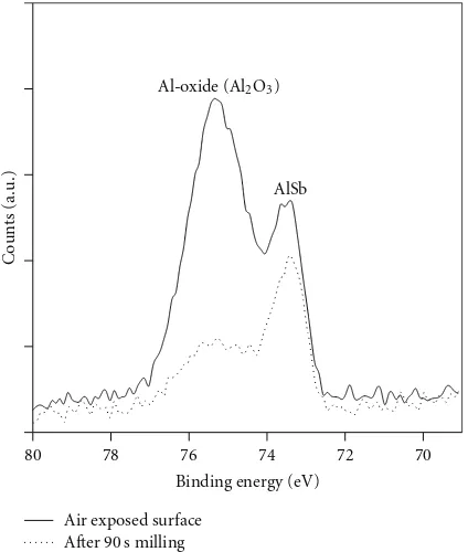
Figure 8shows the XPS Al(2p) spectra obtained from a Al0.05Ga0.95Sb surface before and after 90 seconds of argon
ion milling. For the premilled surface, the Al2O3 exhibits
a high intensity compared to that of the AlSb peak. The ratio of the area shows that at the surface region aluminium exists mainly in the forms of Al2O3, with a small percentage
of AlSb. This occurs because aluminium is very reactive to oxygen. After 90 seconds of milling, a drastic reduction of the Al2O3peak intensity was observed relatively to the AlSb
4. Conclusions
A range of AlxGa1−xSb has been grown by MOCVD with the
Al composition in the range 0 ≤ x ≤ 0.30 with mirror-like surface morphology and good composition control. We have found that the AlxGa1−xSb layers grown at 580◦C and
600◦C and at a V/III ratio of 3 with Al composition in the range of 0.5% and 25% have excellent optical quality with a very high optical transmission at energies below the bandgap. In the low temperature range up to 580◦C, the growth rate depends on temperature (degree of pyrolysis of precursors), and the growth rate of AlGaSb increases monotonically. At high temperatures in the range between 580◦C and 600◦C, the growth rate is constant. Further increasing the growth temperature leads to a decrease of the growth rate due to desorption of gallium and antimony from the growth surface. A growth rate activation energy of 0.73 eV was found. The carrier concentration increases as the growth temperature is increased in the higher growth temperatures from 600◦C up to 680◦C. The rapid increase of carrier concentration in the layer grown at 680◦C may be partially attributed to the increase in the defect density in the layer. The carrier concentration increases and mobility decreases very rapidly as the Al is introduced in small quantities of 0< x <0.025 into the composition. This is thought to be due to AlSb antisite defect and carbon contamination. Further degradation of electrical properties with Al incorporation is not that pronounced. The RT mobility is in the order of 100–426 cm2/V.s and carrier concentration 6.27×10¹⁷–4.48 ×1018cm−3 for compositions in the range of 0.025< x < 0.25. All the samples investigated showed oxide layers (Al2O3,
Sb2O3, and Ga2O5) on the surface layers, the percentage
of aluminium-oxide is especially high compared with a small percentage of AlSb. This indicates that aluminium is very reactive to oxygen from the environment. XPS analysis reveals that carbon and oxygen contents on the surface layers mainly originated from atmosphere exposure.
Acknowledgments
The financial support from the Directorate General of Higher Education (DIKTI), the Ministry of National Edu-cation (DIKNAS), and the Government of the Indonesia Republic is gratefully acknowledged.
References
[1] S. M. Kluth, J. D. Fitz Gerald, and M. C. Ridgway, “Ion-irradiation-induced porosity in GaSb,”Applied Physics Letters, vol. 86, no. 13, Article ID 131920, 3 pages, 2005.
[2] H. Shao, W. Li, A. Torfi, D. Moscicka, and W. I. Wang, “Room-temperature InAsSb photovoltaic detectors for mid-infrared applications,”IEEE Photonics Technology Letters, vol. 18, no. 16, pp. 1756–1758, 2006.
[3] Y. H. Kim, J. Y. Lee, Y. G. Noh, M. D. Kim, and J. E. Oh, “High-resolution transmission electron microscopy study on the growth modes of GaSb islands grown on a semi-insulating GaAs (001) substrate,”Applied Physics Letters, vol. 90, no. 24, Article ID 241915, 3 pages, 2007.
[4] R. Hao, Y. Xu, Z. Zhou et al., “Growth of GaSb layers on GaAs (0 0 1) substrate by molecular beam epitaxy,”Journal of Physics D, vol. 40, no. 4, pp. 1080–1084, 2007.
[5] P.-Y. Wang, J. F. Chen, and W. K. Chen, “Structural and elec-trical properties of GaSb, AlGaSb and their heterostructures grown on GaAs by metalorganic chemical vapor deposition,”
Journal of Crystal Growth, vol. 160, no. 3-4, pp. 241–249, 1996. [6] Y. C. Lin, H. Yamaguchi, E. Y. Chang et al., “Growth of very-high-mobility AlGaSb/InAs high-electron-mobility transistor structure on si substrate for high speed electronic applica-tions,”Applied Physics Letters, vol. 90, no. 2, Article ID 023509, 3 pages, 2007.
[7] C. A. Wang, “Organometallic vapor phase epitaxial growth of AlSb-based alloys,”Journal of Crystal Growth, vol. 170, no. 1–4, pp. 725–731, 1997.
[8] S. K. Haywood, R. W. Martin, N. J. Mason, R. J. Nicholas, and P. J. Walker, “GaSb/InAs heterojunctions grown by MOVPE,”
Journal of Crystal Growth, vol. 107, no. 1–4, pp. 422–427, 1991. [9] F. S. Juang, Y. K. Su, N. Y. Li, and K. J. Gan, “Effects of trimethylantimonide/triethylgallium ratios on epilayer prop-erties of gallium antimonide grown by low-pressure metalor-ganic chemical vapor deposition,”Journal of Applied Physics, vol. 68, no. 12, pp. 6383–6387, 1990.
[10] A. Aardvark, N. J. Mason, and P. J. Walker, “The growth of antimonides by MOVPE,”Progress in Crystal Growth and Characterization of Materials, vol. 35, no. 2–4, pp. 207–241, 1997.
[11] T. Koljonen, M. Sopanen, H. Lipsanen, and T. Tuomi, “Metalorganic vapor phase epitaxial growth of AlGaSb and AlGaAsSb using all-organometallic sources,”Journal of Crystal Growth, vol. 169, no. 3, pp. 417–423, 1996.
[12] Ch. Ungermanns, H. Hardtdegen, M. Matt et al., “MOMBE and characterization of InAs and (Al,Ga)Sb,”Journal of Crystal Growth, vol. 188, no. 1–4, pp. 32–38, 1998.
[13] H. Asahi, T. Kaneko, Y. Okuno, and S. Gonda, “Improved growth kinetic model for metalorganic molecular beam epitaxy using triethylgallium,” Japanese Journal of Applied Physics, Part 1, vol. 32, no. 6, pp. 2786–2793, 1993.
[14] T. Koljonen, M. Sopanen, H. Lipsanen, and T. Tuomi, “Growth of high-quality GaSb by metalorganic vapor phase epitaxy,”
Journal of Electronic Materials, vol. 24, no. 11, pp. 1691–1696, 1995.
[15] Y. Okuno, H. Asahi, T. Kaneko, Y. Itani, K. Asami, and S. Gonda, “MOMBE growth of AlGaSb,” Journal of Crystal Growth, vol. 115, no. 1–4, pp. 236–240, 1991.
[16] J. M. Kang, M. Nouaoura, L. Lassabat`ere, and A. Rocher, “Accommodation of lattice mismatch and threading of dislo-cations in GaSb films grown at different temperatures on GaAs (001),”Journal of Crystal Growth, vol. 143, no. 3-4, pp. 115– 123, 1994.
[17] F. Pascal, F. Delannoy, J. Bougnot et al., “Growth and characterization of undoped and N-type (Te) doped MOVPE grown gallium antimonide,”Journal of Electronic Materials, vol. 19, no. 2, pp. 187–195, 1990.
[18] S. C. Chen and Y. K. Su, “Photoluminescence study of gallium antimonide grown by liquid-phase epitaxy,”Journal of Applied Physics, vol. 66, no. 1, pp. 350–353, 1989.
[19] M.-C. Wu, C.-W. Chen, and C.-C. Chen, “Growth-tempera-ture dependence of electrical and luminescent properties of high-quality GaSb grown by liquid-phase epitaxy,”Journal of Applied Physics, vol. 72, no. 3, pp. 1101–1103, 1992.
[21] E. T. R. Chidley, S. K. Haywood, R. E. Mallard et al., “GaSb heterostructures grown by MOVPE,”Journal of Crystal Growth, vol. 93, no. 1–4, pp. 70–78, 1988.
[22] J. F. Moulder, W. F. Stickle, P. E. Sobol, and K. D. Bomben,