Faculty of Electrical Engineering
ANALYSIS AND SIMULATION OF THREE PHASES
Z SOURCE INVERTER
Nur Saiyidah Binti Anas
Bachelor of Electrical Engineering (Power Electronic & Drives)
ANALYSIS AND SIMULATION OF THREE PHASES Z SOURCE INVERTER
NUR SAIYIDAH BINTI ANAS
A report submitted in partial fulfillment of the requirements for the degree of Bachelor of Electrical Engineering (Power Electronic & Drives)
Faculty of Electrical Engineering
UNIVERSITI TEKNIKAL MALAYSIA MELAKA
ANALYSIS AND SIMULATION OF THREE PHASES Z SOURCE INVERTER
NUR SAIYIDAH BINTI ANAS
A report submitted in partial fulfillment of the requirements for the degree of Bachelor of Electrical Engineering (Power Electronic & Drives)
Faculty of Electrical Engineering
UNIVERSITI TEKNIKAL MALAYSIA MELAKA
DECLARATION
I declare that this report entitled “Analysis and Simulation of three phases Z Source Inverter” is the result of my own research except as cited in the references. The report has not been accepted for any degree and is not concurrently submitted in candidature of any other degree.
Signature : ...
Name : Nur Saiyidah binti Anas
APPROVAL
“ I hereby declare that I have read through this report entitle “Analysis and Simulation of
three phases Z Source Inverter” and found that it has comply the partial fulfillment for
awarding the degree of Bachelor of Electrical Engineering (Power Electronic & Drives)”
Signature : ...
Supervisor‟s Name : Puan Norhazilina binti Bahari
DEDICATION
Dedicated, in thankful appreciation for support, encouragement and understanding to:
My beloved father Anas bin Abd Kadir and mother Hanisah binti Hj Sobri;
my sisters;
and all my friends;
ACKNOWLEDGMENT
Thanks to Allah S.W.T because without His blessings and guidance for giving me inspiration and strengths to complete this project with good health until the last day of the project report has been submitted.
I express my gratitude and thanks to my supervisor, Pn. Norhazilina binti Bahari for
her consistent encouragement, advice and invaluable guidance throughout the entire course of
this research project. I also would like to thank my fellow friends who always helping me to figure out my mistake and give support during my project.
Not forgotten, I would like to express my gratitude to Dr Auzani bin Jidin for sharing his valuables ideas as well as his knowledge. Most importantly, I would like to thank my family for their love, sacrifice, motivation and continuous support during my graduate school experience.
iii
ABSTRACT
This project involves on the analysis and simulation of three phases Z Source Inverter (ZSI). The application of ZSI is widely used in industry such as photovoltaic, general motor drive and fuel cell. The new power inverter have been introduced to overcome the problem in conventional inverter which is has some limitation in term of boosting voltage. Inverter consists of two types of conventional inverter known as Voltage Source Inverter (VSI) and Current Source Inverter (CSI). However, both inverters are having some limitations. The limitation of the inverter is cannot fully utilize the available DC link voltage to enhance output voltage. The maximum output voltage at modulation index, 1.0 using Sinusoidal Pulse Width Modulation (SPWM) technique is limited at half of the DC link voltage. Besides that, the output voltage of conventional inverter is lower or equal than desired voltage. In other word, the voltage drop is higher compared with ZSI by using conventional inverter. The main purpose of this project is to analyze the performance of total harmonic distortion and maximum output voltage for various modulation indexes by using MATLAB software. This project is more focuses on Simple Boost technique and the sequence of this project begin with derive the equation. In order to control the output voltage is greater than input, boost factor had been implemented by varying modulation index. The simple boost switching circuit is designed to allow shoot through occur. The modulation index of simple boost is depending on upper voltage (Vp) and lower voltage (Vn). By comparing the modulation index, 0.8 between simple boost and SPWM, it shows that improvement about 67.24 %. Even though the modulation index of simple boost is low than SPWM, the capability of boosting output voltage by using simple boost is more effective.
ABSTRAK
v
2.2.2 Inverter problem 5
2.3 Current Source Inverter (CSI) 6
vii
4 RESULT AND DISCUSSION 34
4.1 Introduction 34
4.2 Parameter of ZSI Simulation Model 34
4.3 Simulation Result of Conventional Inverter 35
4.4 Simulation Result of Z Source Inverter 38
4.5 Mathematical Derivation 42
4.6 Performance Analysis of Maximum Voltage 45
4.7 Performance Analysis of Total Harmonic 50
Distortion of maximum voltage (THDv) by using SPWM and Simple boost 5 CONCLUSION & RECOMMENDATION 52
REFERENCES 54
LIST OF TABLES
TABLE TITLE PAGE
2.1 The Characteristic of CSI, VSI and ZSI 16
3.1 The switching patterns in a three-phase inverter, 25
xi
4.8 Line to neutral voltage waveform of ZSI 40
4.9 Inverter voltage waveform of ZSI 40
4.10 Phase current waveform of ZSI 41
4.11 Inverter voltage waveform in term of V inverter, 41
L1& L2 and C1 &C2 of ZSI 4.12 Graph of maximum voltage using SPWM and 47
Simple boost (Calculation) 4.13 Graph of maximum voltage using SPWM and 49
Simple boost (Simulation) 4.14 Graph of Total Harmonic Distortion (THDv) 51
based on simulation by using SPWM and
APPENDIX TITLE PAGE
A RESEARCH FRAMEWORK OT (RFOT)** 57
B TURNITIN REPORT 59
C GANTT CHART PSM 1 60
1
CHAPTER 1
INTRODUCTION
1.1 Project Background
Inverter is the device to convert power supply from input dc in the form of current or voltage to variable output ac voltage. There are two techniques to control the variable output ac voltage. The technique are either varying the gain of the inverter or varying the input dc power supply. In industry, the two types of inverter are familiar used for many applications namely Voltage Source Inverter (VSI) and Current Source Inverter (CSI).
The input source connected in parallel with a large dc capacitor in main circuit of VSI. The main function of dc capacitor is as the filtering element to block voltage ripple, provide temporary storage and sole energy storage. Battery or diode rectifier can be the input dc power supply of the circuit. Different with CSI circuit, the input source connected in series with a large inductor. DC inductor is the filtering component to block current ripple or sole energy storage and provide temporary storage. However, both of the inverters have the problems. The problems are both of the inverter cannot be a buck boost inverter, cannot be interchangeable and vulnerable to electromagnetic interface (EMI).
simulation will be model by using MATLAB Simulink. This project is more focuses on step up the voltage and analyzes the ZSI by using simple boost control techniques.
1.2 Project Motivation
In most of the industries, traditional Inverter is normally used in adjustable speed drives application. However, the inverter has some limitations and problem. For example in VSI, the upper and lower switch cannot be switched on at the same time. If the situation occurs, it may cause the shoot through and damage in the inverter circuit. The problem of the traditional inverter will be improved by using ZSI. Nowadays, the new power inverter is widely used such as in utility, domestic and traction applications. The new inverter not only used in adjustable speed drives application but can be used for other application. The most popular application used on this inverter is for fuel cell, general motor drive and photovoltaic applications.
1.3 Problem Statement
There are some problems of the traditional inverter which are both of the inverter cannot be a buck boost inverter. It is because the traditional inverter only has one function neither buck inverter nor boost inverter. The other problem is the main circuit of VSI and CSI cannot be interchangeable. For the example, the main circuit of VSI cannot be used in CSI circuit. Furthermore, the traditional inverter also exposed to Electromagnetic Interface (EMI) noise.
1.4 Objective
1) To analyze the performance of total harmonic distortion and power factor by
using MATLAB.
3
1.5 Project Scope
To prove the data from the theoretical, simulation from MATLAB is needed. After that, the results can be compared with the calculation or theoretical values. In this project, student should be able:
1. To analyze how the traditional inverter can be combined together.
2. To make sure either the power factor varies to be more efficient or not between
the traditional inverter and three phases of ZSI.
3. To identify the method of ZSI to control the shoot-through and switching
pattern.
4. To analyze the Total Harmonic Distortion (THD) either can reduce THD and
able to smooth the waveform of inverter.
5. To identify the limit range of the ZSI.
1.6 Report Outlines
The aim of this project is to analyze and simulate the three phases of ZSI.
Chapter 1 will represent about this project. This chapter include of the overview of project background, project motivation, problem statement, objective and the project scope.
Chapter 2 will focuses on the theoretical of traditional inverter and three phase of ZSI. This chapter also will discuss about the related previous work and make the comparison.
Chapter 3 will discusses about the methodology of the project. This chapter also will explain about the mathematical derivation and the flow or step to analyze the system work and circuit design.
Chapter 4 will explains and discusses all the results obtained and the analysis of the project. This topic also includes the comparisons of expected results and simulation results between traditional inverter and Z Source Inverter.
CHAPTER 2
LITERATURE REVIEW
2.1 Introduction
This chapter will discuss about the theoretical, mathematical derivation and all the information data related to the three phase ZSI. In order to solve the problem toward the traditional inverters, the characteristic of traditional inverter will be compared with ZSI. The theoretical will be the guidelines to complete and analyze the simulation of this project.
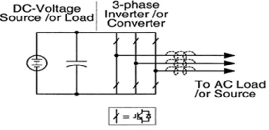
2.2 Voltage Source Inverter (VSI)
2.2.1 Construction circuit
5
Figure 2.1: Construction circuit (VSI)
2.2.2 Inverter problem
Although the voltage inverter circuit has been widely used, it still has some limitations [3]. The following are the problem of the inverter:
1. The circuit is only able to step down the voltage from DC to AC. In other
words, the output in form of alternative current (AC) is limited voltage and cannot exceed the DC input voltage [4].
2. Each phase leg of the inverter (upper and lower devices) cannot be gated on
at the same time. This limitation requires the circuit to have dead time where it will ensure that shoot-through does not occur and destroy the devices. Unfortunately, dead time contributes to waveform distortion [4].
3. An output low pass filter is required which causes control complexity and
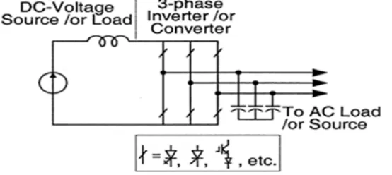
2.3.1 Construction circuit
The construction circuit of the three phase inverter is shown in figure 2.2. The circuit consists of six self commutated semiconductor switches with the anti parallel diode and a power transistor. The semiconductor switching devices would provide bidirectional voltage blocking and unidirectional current [1].
Figure 2.2: Construction circuit (CSI)
2.3.2 Inverter problem
The following are the theoretical and conceptual limitations of the inverter:
1. The inverter is a step down rectifier for AC to DC power conversion and
step up inverter for DC to AC power conversion. In other words, the DC voltage produced is always less than input voltage in form of AC. An additional DC to DC buck inverter is needed for applications where a wide voltage range is desirable. It will cause lowers efficiency and system cost increases [4].
2. The switch from upper and lower should at least maintained and have to be
7
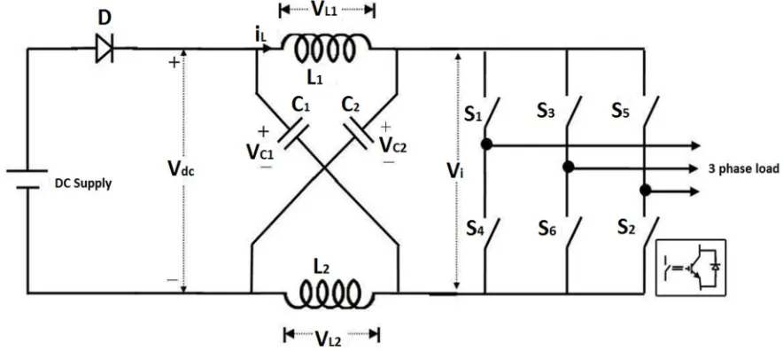
2.4 Z Source Inverter
2.4.1 Construction circuit
Based on the configuration circuit in figure 2.3, ZSI is connected between the inverter to DC supply and load. A two port network that consists of two
capacitor( , ) and two inductor( , ) connected in X shape [5]. DC supply or
load can be whether a current, voltage or load. DC power supply can be a battery, capacitor, thyristor, an inductor and so on [1]. The inverter that uses switches can be series combination and the anti-parallel combination. ZSI has a better characteristic if compared with the traditional inverter [6].