Design Minkowski Shaped Patch Antenna with
Rectangular Parasitic Patch Elements for 5.8 GHz
Applications
H. Nornikman, B. H. Ahmad, M. Z. A. Abd Aziz, A. R. Othman, M. A. Azlishah
Center for Telecommunication Research and Innovation (CeTRI), Faculty of Electronics and Computer Engineering Universiti Teknikal Malaysia Melaka (UTeM)
Durian Tunggal, Melaka, Malaysia
[email protected], [email protected], [email protected], [email protected], [email protected]
F. Malek
School of Electrical Systems Engineering Universiti Malaysia Perlis (UniMAP)
Pauh Putra, Perlis, Malaysia [email protected]
Abstract—This paper presents the parametric study on the Minkowski shaped antenna with the rectangular parasitic patch elements. This patch antenna consists four parts – patch, feed line, ground plane and parasitic elements. The rectangular parasitic patch elements are located at the bottom of the Minkowski shaped patch. The parametric study of different patch sizes (Design 2A, Design 2B, Design 2C, Design 2D and Design 2E) is presented in this paper. The antenna parameters studied in this paper are resonant frequencies, return loss at the resonant frequency, bandwidth and realized gain. The target frequency of this antenna is 5.80 GHz for Worldwide Interoperability for Microwave Access (WiMAX) application. It shows the return loss of – 24.477 dB, bandwidth of 254 MHz (5.676 GHz to 5.930 GHz) and a gain of 2.351 dB.
Index Terms—Minkowski; patch antenna; gain; return loss; bandwidth
I.INTRODUCTION
Wireless telecommunication system has become common needs in the nearly two decades. This system provides freedom in convenience and lifestyle to support faster data transfer, smaller in size and mobility devices. A quality of the antenna depends on the gain, radiation pattern, efficiency and the bandwidth result.
Worldwide Interoperability for Microwave Access (WiMAX) is a wireless communication standard had been established by the IEEE 802.16 (fixed WiMAX) and IEEE 802.16e (Mobile WiMAX). WiMAX is grouped in the three different frequency bands that is 2.300 GHz to 2.690 GHz for low frequency band, 3.200 GHz to 3.800 GHz for the middle frequency band, and lastly upper frequency band with 5.200 GHz to 5.800 GHz. Mobile WiMAX applications operate
efficiently at a frequency of 2.300 GHz (frequency range of 2.300 GHz to 2.400 GHz) [1]. WiMAX has potential to replace global system for mobile (GSM) communication in the current cellular technologies.
The microstrip patch antenna is the best selection for the researcher because it is a low cost material, lightweight and also easy to fabricate. Many investigators had been enhanced antenna's performance of gain, resonant frequency, return loss, directivity and also the bandwidth. This improvement work probably can use many types of several shapes of antennas, the added special structure into the patch antenna, put of RF components and added integrated circuit (IC) into the patch antenna [2]. The examples structures are split ring resonator (SRR), defected ground structure (DGS) [3], electromagnetic band gap (EBG) [4], parasitic element [5] and fractal geometry shapes [6].
Fractals geometry shape can be composed by applying multiple copies of the similarity structure with different size and scale. Fractal geometry like Minkowski, Sierpinski gasket [7], Tee fractal, Hilbert curve fractal [8], box meander-line, meander-line planer, Giuseppe Peano fractal [9] and Koch fractal [10], and other fractal elements potentially to miniaturize the antenna and increase the bandwidth of the patch antenna. Minkowski island [11] and Minkowski-like pre-fractal (MLPF) [12] is the hybrid design of the Minkowski shaped fractal.
Figure 1 shows the early stages of Minkowski shaped patch antenna that had been proposed in [13]. This Minkowski shaped antenna was designed using FR-4 substrates with permittivity, εr = 4.3. The finishing dimension after optimization work for the modified Minkowski patch antenna is 34.0 mm width and 45.0 mm length. The thickness of this
substrate is 1.6 mm. The copper thickness for both patch and ground layer is 0.035 mm.
Fig. 1. Schematic diagram of previous Minkowski shaped patch antenna design (Design 1) by [13]
Figure 2 and Table I show the return loss of the Minkowski shaped patch antenna for 2.400 GHz applications. The resonant frequency of this antenna is at 2.404 GHz with a return loss of – 47.990 dB. The return loss at 2.400 GHz is – 33.140 dB, lower that the result in resonant frequency point. The gain at the resonant frequency of 2.404 GHz is 2.445 dB while the gain at 2.400 GHz is 2.448 dB.
Return Loss of Minkowski Patch Antenna
Frequency, dB
2.2 2.3 2.4 2.5 2.6
Re
tur
n
l
o
ss
, dB
-50 -40 -30 -20 -10 0
Modified Minkowski
Fig. 2. Return loss of Minkowski shaped patch antenna design by [13]
TABLE I.DIMENSION OF THE MINKOWSKI SHAPED PATCH ANTENNA WITH PARASITIC PATCH ELEMENTS
Antenna Resonant frequency,
fr (GHz)
Return loss (dB) at
fr
Return loss (dB) at 2.400 GHz
Minkowski patch antenna [13]
2.402 - 47.990 - 33.140
The goal of this paper is to investigate the effect of the parasitic patch elements to the Minkowski shaped patch antenna design. The target frequency of this antenna is 5.800 GHz with a return loss must be better than – 10 dB.
II.ANTENNA DESIGN
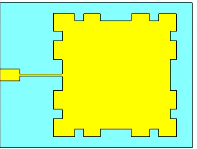
Figure 3 shows the schematic diagram of the modified Minkowski shaped patch antenna with rectangular parasitic patch elements. Table II shows the dimension of the modified Minkowski patch antenna. The dimension of the FR-4 substrate is 19.20 mm width x 25.80 mm length x 1.60 mm thickness. Compared with the previous work, this antenna had been miniaturized 67.62 % of the FR-4 substrate size.
Fig. 3. Schematic diagram of Minkowski shaped patch antenna with parasitic patch elements
TABLE II.DIMENSION OF THE MINKOWSKI SHAPED PATCH ANTENNA WITH PARASITIC PATCH ELEMENTS
Part Symbol Dimension (mm)
Antenna 1 [13]
Antenna 2
Substrate width WS 34.00 19.20
Substrate length LS 45.00 25.80
Patch width Wp 28.86 11.13
Patch length Lp 28.86 11.13
Feed width Wf 2.81 2.87
Feed length Lf 14.50 10.50
Combined parasitic width
Wc - 4.70
Combine parasitic length
Lc - 9.10
Parasitic width Wx - 0.50
Parasitic length Lx - 2.98
Parasitic gap Gx - 0.10
Ws Ls
Lp
Wp
Wf Lf
Lx
Parasitic patch elements that attach to the antenna are another technique to improve the patch antenna performance. The parasitic elements are designed to widen the bandwidth of the patch antennas [14]. The examples on the patch antenna using parasitic elements are L-band parasitic element [15], circular parasitic element [16] the spiral parasitic element [17] and inverted-L parasitic element [18].
This Minkowski shaped patch antenna consists four parts – patch, feed line, ground plane and rectangular parasitic elements. This patch antenna has the feeding structure of a 50 ohm microstrip line. The feed line is located between the rectangular parasitic patch elements and the bottom part of the patch antenna. This patch antenna is printed on the FR-4 substrate with dielectric constant, εr =4.3. The thickness of the substrates is 1.60 mm while the thickness of the copper is 0.035 mm, same with the previous design. The ground plane consists of the copper with same dimension of the patch antenna.
TABLE III.A PARAMETRIC STUDY ON THE DIFFERENT PATCH DIMENSION (WIDTH AND LENGTH) OF MINKOWSKI SHAPED ANTENNA WITH PARASITIC
PATCH ELEMENTS
Antenna design Patch width (mm) Patch length (mm)
2A 10.010 10.010
2B 10.570 10.570
2C 11.130 11.130
2D 11.690 11.690
2E 12.250 12.250
The square patch part dimension is 11.13 mm width x 11.13 mm length (85.13 % of the Minkowski shaped patch antenna size). This patch part is located at the top of the substrate, connected to the feed line. The feed line is 10.50 mm in length and also 2.870 mm width. These parasitic elements are located below than Minkowski patch antenna element. There are eight same size dimensions of a rectangular patch in the first row with 0.1 mm gap between each other. A single unit of the rectangular parasitic patch element dimension is 0.5 mm width x 2.975 mm long. Table III shows the parametric study on the different patch dimension of Minkowski shaped antenna with parasitic patch elements.
III.RESULT
This section is discussed on the resonant frequency, return loss, realized gain, and bandwidth performance of the Minkowski patch antenna with rectangular parasitic patch elements. The return loss of normal modified Minkowski patch antenna (without any patch dimension changes) had
been shown in Figure 4.
The resonant frequency of this design is 5.800 GHz with - 24.472 dB of return loss. The - 10 dB bandwidth of this design is 0.254 GHz at the frequency between 5.676 GHz and 5.930 GHz.
Return Loss of Modified Minkowski Patch Antenna with Rectangular Patch Antenna
Frequency, GHz
Fig. 4. Return loss of Minkowski shaped patch antenna with parasitic rectangular patch antenna
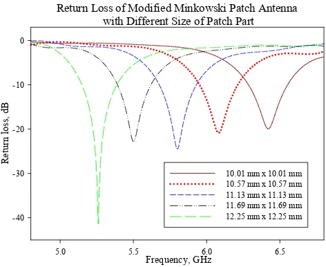
Figure 5 shows the return loss of modified Minkowski patch antenna with different size of patch part. From the graph, it shows that the additional of patch antenna dimension will decrease frequency resonant in the lower range while the reducing the size can effect higher range of resonant frequency.
Return Loss of Modified Minkowski Patch Antenna with Different Size of Patch Part
Frequency, GHz
Fig. 5. Return loss of Minkowski patch antenna with different size of patch antenna (width and length)
size, the frequency had been shifted from 5.80 GHz to 5.26 GHz. The decrement 1.12 mm width x 1.12 mm length of the patch size, the frequency had been shifted from 5.80 GHz to 6.42 GHz.
TABLE IV.RESONANT FREQUENCY AND RETURN LOSS OF THE MINKOWSKI SHAPED PATCH ANTENNA WITH PARASITIC PATCH ELEMENT
Antenna design
Resonant frequency,
fr (GHz)
Return loss (dB)
Bandwidth (MHz),
f1-f2 (GHz)
Return loss (dB)
2A 6.420 - 19.954 267 (6.285 – 6.552)
2.697
2B 6.082 - 20.830 260 (5.951 – 6.212)
2.331
2C 5.800 - 24.472 254 (5.676 – 5.930)
2.351
2D 5.502 - 22.874 229 (5.391 – 5.620)
2.170
2E 5.260 - 41.421 238 (5.148 – 5.387)
2.034
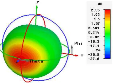
The best return loss shown by the antenna Design 2E with – 41.421 dB at resonant frequency of 5.260 GHz compare to the normal design (Design 2C) with only - 24.472 dB at resonant frequency of 5.80 GHz. The best gain had been shown by Design 2A with 2.697 dB, additional 0.346 dB compares to the normal design of Design 2C. Design 2A is a wider bandwidth result of compared with all design. The bandwidth for this design is 267 MHz. The normal design with only 254 MHz of bandwidth. Figure 6 shows the 3D radiation pattern of the Minkowski shaped patch antenna with parasitic rectangular patch antenna. This figure shows the signal is radiated frontside from the patch antenna.
This antenna can be improved its gain performance by adding the split ring resonator structure into the patch design. It also can reduce the size of the patch antenna significantly such as in [19-20].
Fig. 6. 3D radiation pattern of Minkowski shaped patch antenna with parasitic rectangular patch antenna (normal design with resonant frequency of 5.800 GHz)
Figure 7 represents the 3D radiation pattern for the Minkowski shaped patch antenna (Design 2C) that resonate at 5.800 GHz with gain performance of 2.351 dB. It shows that the current flow is focusing at the patch antenna, feed line and the parasitic elements. The strong current flow is located at the outer border of the patch antenna part.
Fig. 7. Surface current of Minkowski patch antenna with parasitic rectangular patch antenna
IV.FUTURE WORKS
The proposed Minkowski shaped antenna design will be integrated with RF transmitter [21] and RF receiver [22] to form a complete RF front-end transceiver system. In the transceiver system the antenna will be integrated with the other subcomponents such as filters [23], amplifiers [24], switch [25], mixer [26] and oscillator [27].
V.CONCLUSION
This Minkowski shaped patch antenna successfully operates in the frequency range of WiMAX application. From the simulation work in CST Microwave Studio simulation software, different dimension of patch effect the return loss, resonant frequency, bandwidth, and realized gain of the Minkowski patch antenna with the rectangular parasitic elements.
REFERENCES
[1] M. Jusoh, M. F. Jamlos, H. A. Rahim, M. F. A. Malek, M. R. Kamarudin, and M. R. Hamid, “Reconfigurable Beam Steer Antenna (RBSA) Design for WiMAX Application,” 2012 Loughborough Antennas and Propagation Conference (LAPC), pp. 1 - 4, 2012.
[3] Z. Zakaria, N. A. Shairi, R. Sulaiman, and W. Y. Sam, “Design Of Reconfigurable Defected Ground Structure (DGS) for UWB Application,” 2012 IEEE Asia-Pacific Conference on Applied Electromagnetics (APACE), pp. 195-198, 2012.
[4] O. Ayop, M. K. A. Rahim, T. Masri, M. N. A. Karim, and M. Z. A. A. Aziz, “Modified Slotted Patch Electromagnetic Band Gap for Antenna Array Application,” Asia-Pacific Microwave Conference (APMC 2007), pp. 1 - 4, 2007
[5] S. M. Kayat, M. T. Ali, M. K. M. Salleh, N. Ramli, M. H M. Rusli, “Reconfigurable Truncated Rhombus-like Microstrip Slotted Antenna with Parasitic Elements,” 2013 7th European Conference on Antennas and Propagation (EuCAP), pp. 898-902, 2013.
[6] N. A. Saidatul, A. A. H. Azremi, R. B. Ahmad, P. J. Soh, and F. Malek, “Multiband Fractal Planar Inverted F antenna (F-PIFA) for Mobile Phone Application,” Progress In Electromagnetics Research B (PIER B), vol. 14, pp. 127 - 148, 2009
[7] K. Ismail, S. . Ishak, “Sierpinski Gasket Fractal Antenna with Defected Ground Structure (DGS),” 2012 International Conference on ICT Convergence (ICTC), pp. 441-446, 2012.
[8] S. Suganthi, S. Raghavan, D. Kumar, and S. Hosimin Thilagar, “A Compact Hilbert Curve Fractal Antenna On Metamaterial Using CSRR”, Progress in Electromagnetics Research Symposium (PIERS), pp. 136-140, 2012.
[9] H. Oraizi and S. Hedayati, “Miniaturization of Microstrip Antennas By The Novel Application of the Giuseppe Peano Fractal Geometries”, IEEE Transactions on Antennas and Propagation, vol. 60, issue 8, pp. 3559 - 3567, 2012
[10] A. Ismahayati, P. J. Soh, R. Hadibah, and G. A. E. Vandenbosch, “Design and Analysis Of a Multiband Koch Fractal Monopole Antenna,” 2011 IEEE International RF and Microwave Conference (RFM), pp. 58-62, 2011.
[11] Q. Luo, H. M. Salgado, and J. R. Pereira, “Fractal Monopole Antenna Design Using Minkowski Island Geometry,” IEEE Antennas and Propagation Society International Symposium, (APSURSI '09), pp. 1-4, 2009
[12] E. C. Lee, P. J. Soh, N. B. M. Hashim, and G. A. E. Vandenbosch, H. Mirza, I. Adam, S. L. Ooi, “Design of a Flexible Minlowski-Like Pre Fractal (MLPF) Antenna with Different Ground Planes for VHF LMR,” 2011 International Workshop on Antenna Technology, pp. 298-301, 2011.
[13] F. Malek, M. S. Zulkifli, N. A. M. Affendi, N. Saudin, H. Nornikman, H. M Mat, L. Mohamed, A. A. Ali, “Complementary Structure of Quadruple P-Spiral Split Ring Resonator (QPS-S) on Modified Minkowski Patch Antenna Design,” 2012 IEEE Asia-Pacific Conference on Applied Electromagnetics (APACE 2012), pp. 142 -147, 2012.
[14] F. Fezai, C. Menudier, M. Thevenot, and T. Monediere, “Compact Directive Parasitic Element Antenna for Wireless Communications Systems,” 2012 15th International Symposium on Antenna Technology and Applied Electromagnetics (ANTEM), pp. 1 - 4, 2012.
[15] L. Akhoondzadeh-Asl, and J. Laurin, “Dual-Mode L-Band Switched Parasitic Element Antenna for Avionics Applications,”
2012 IEEE Antennas and Propagation Society International Symposium (APSURSI), pp. 1 - 2, 2012.
[16] O. Ayop, M. K. A. Rahim, and T. Masri, “Planar Dipole Antenna with and without Circular Parasitic Element,” Asia-Pacific Conference on Applied Electromagnetics (APACE 2007), pp. 1 - 4, 2007
[17] T. Tsukiji and Y. Kumon, “A Simple Circularly Polarized Wave Antenna using a Modified Transmission Line Antenna and Spiral Parasitic Element,” 16th IST Mobile and Wireless Communications Summit, pp. 1 - 5, 2007.
[18] K.-B. Kim, H.-K. Ryu, and J.-M. Woo, “Compact Wideband Folded Monopole Antenna Coupled with Parasitic Inverted-L Element for Laptop Computer Applications,” Electronics Letters, vol. 47, issue 5, pp. 301 - 303, 2011
[19] S. S. Karthikeyan and R S.. Kshetrimayum, “Performance Enhancement of Microstrip Bandpass Filter Using CSSRR,” International Conference on Advances in Computing, Control, & Telecommunication Technologies, (ACT '09), pp. 67 - 70, 2009.
[20] H. A. Majid, M. K. A. Rahim, and T. Masri, “Microstrip Antenna's Gain Enhancement Using Left-Handed Metamaterial Structure,” Progress In Electromagnetics Research M (PIER M), vol. 8, 235 - 247, 2009.
[21] N. A. Shairi, T. A. Rahman, M. Z. A. Abd Aziz, "RF Transmitter System Design for Wireless Local Area Network bridge at 5725 to 5825 MHz," International Conference on Computer and Communication Engineering (ICCCE 2008), pp. 109 - 112, 2008.
[22] N. A. Shairi, T. A. Rahman, M. Z. A. Aziz, "RF Receiver System Design for Wireless Local Area Network Bridge at 5725 to 5825 MHz," Asia-Pacific Conference on Applied Electromagnetics (APACE 2007), pp.1 - 6, 2007.
[23] Z. Zakaria, W. Y. Sam, M. Z. A. Abd Aziz, M. A. Meor Said, M "Microwave Filter and Antenna for Wireless Communication Systems," 2012 IEEE Symposium on Wireless Technology and Applications (ISWTA), pp. 75 - 80, 2012.
[24] M. H. Misran, M. A. Meor Said, K. G. Cheng, M. A. Othman, M. M. Ismail, H. A. Sulaiman, "Design of Gaas E-phemt Low Noise Amplifier for WLAN Application," 2012 International Conference on Green and Ubiquitous Technology (GUT), pp. 106 - 109, 2012.
[25] N. A. Shairi, B. H. Ahmad, A. C. Z. Khang, "Design and Analysis of Broadband High Isolation of Discrete Packaged PIN Diode SPDT Switch for Wireless Data Communication," 2011 IEEE International RF and Microwave Conference (RFM), pp. 91 - 94, 2011.
[26] C.- H. Chen, P.- Y. Chiang, C. F. Jou, "A Low Voltage Mixer With Improved Noise Figure," IEEE Microwave and Wireless Components Letters, vol. 19, no.2, pp. 92 - 94, 2009.