DESIGN OF MICROSTRIP ANTENNA WITH PARASITIC ELEMENT
MUHAMMAD HAKIM BIN HARUN
This report is submitted in partial fulfillment of the requirements for the award of the Bachelor of Electronic Engineering (Electronic Telecommunication) With
Honors
Faculty of Electronic and Computer Engineering Universiti Teknikal Malaysia Melaka
ii
UNIVERSTI TEKNIKAL MALAYSIA MELAKA
FAKULTI KEJURUTERAAN ELEKTRONIK DAN KEJURUTERAAN KOMPUTER
BORANG PENGESAHAN STATUS LAPORAN PROJEK SARJANA MUDA II
Tajuk Projek : ………
Sesi
Pengajian : 2009/2010
Saya
……….. (HURUF BESAR)
mengaku membenarkan Laporan Projek Sarjana Muda ini disimpan di Perpustakaan dengan syarat-syarat kegunaan seperti berikut:
1. Laporan adalah hakmilik Universiti Teknikal Malaysia Melaka.
2. Perpustakaan dibenarkan membuat salinan untuk tujuan pengajian sahaja.
3. Perpustakaan dibenarkan membuat salinan laporan ini sebagai bahan pertukaran antara institusi pengajian tinggi.
4. Sila tandakan ( √ ) :
SULIT*
*(Mengandungi maklumat yang berdarjah keselamatan atau kepentingan Malaysia seperti yang termaktub di dalam AKTA RAHSIA RASMI 1972)
TERHAD** **(Mengandungi maklumat terhad yang telah ditentukan oleh organisasi/badan di mana penyelidikan dijalankan)
TIDAK TERHAD
Disahkan oleh:
__________________________ ___________________________________
(TANDATANGAN PENULIS) (COP DAN TANDATANGAN PENYELIA)
Alamat Tetap: LOT 520, KG. BKT PAYUNG,
06400 ALOR STAR, KEDAH DARUL AMAN.
Tarikh: ……….. Tarikh: ………..
DESIGN OF MICROSTRIP ANTENNA WITH PARASITIC ELEMENT
MUHAMMAD HAKIM BIN HARUN
iii
“I hereby declare that this report is the result of my own except for quotes as cited in the references”
Signature :
Author : Muhammad Hakim Bin Harun
iv
“I hereby declare that I have read this report and in my opinionthis report is sufficient in terms of the scope and quality for the award of Bachelor of Electronic Engineering
(Telecommunication Electronics) With Honours.”
Signature :
Supervisor’s Name : Mr. Mohamad Zoinol Abidin Abd Aziz
v
vi
ACKNOWLEDGMENTS
First of all, I am most grateful to Almighty ALLAH s.w.t. for blessing me with good health and ideas in completing this research successfully. I would like to thank Allah for HIS firm hands in guiding me in the course of completing this thesis writing. Alhamdulillah.
I would like to show my highest gratitude to my supervisor, Mr Mohamad Zoinol Abidin Abd Aziz for his invaluable support, patient, assistance and especially his encouragement to this project. I truly have learnt a lot and all this would not be without his guidance.
I also would like to thank all my fellow friends for their contribution in giving me a moral support throughout my project development period. Last but not least, to all my beloved family members who were always, stand by my side to encourage, advice, comfort, cherish, and support me during this entire project.
vii
ABSTRACT
viii
ABSTRAK
ix
TABLE OF CONTENTS
CHAPTER TITLE PAGE
TITLE OF THE PROJECT i
DISCLAIMER ii
DECLARATION iii
SUPERVISOR’S CONFIRMATION iv
DEDICATION v
ACKNOWLEDGMENT vi
ABSTRACT vii
ABSTRAK viii
TABLE OF CONTENTS ix
LIST OF TABLE xiii
LIST OF FIGURE xv
LIST OF ABBREVIATIONS xvii
I INTRODUCTION
1.1 Project Background 1
1.2 Project Objective 2
1.3 Problem Statement 2
1.4 Scope of Work 2
1.5 Project Methodology 3
II LITERATURE REVIEW
2.1 Project Flow 4
2.2 Introduction of Antenna 6
2.3 Antenna Parameters 6
x
2.3.2 Quality Factor 8
2.3.3 Bandwidth 8
2.3.4 Resonant Frequency 9
2.3.5 Input Impedance 9
2.3.6 Return Loss 10
2.3.7 Polarization 10
2.3.7.1 Linear Polarization 10
2.3.7.2 Circular Polarization 11
2.4 Microstrip Patch Antenna 11
2.4.1Fundamental Specifications Of Patch Antennas 13
2.4.1.1Radiation Pattern 13
2.4.1.2Antenna Gain 14
2.4.1.3Polarization 15
2.4.1.4Bandwidth 16
2.4.1.5Alternative Feed Type 17
2.5 Microstrip Rectangular Patch Antenna 20 2.6 Microstrip Rectangular Patch Antenna 22
2.7 Parasitic Element 24
III METHODOLOGY
3.1 Design Consideration 27
3.1.1The Dielectric Constant 27
3.1.2Feed Line 28
3.1.3Substrate Thickness 28
3.2 Design Of Microstrip Parasitic Antenna 29
3.2.1Design 1 29
3.2.2Design 2 31
3.2.3Design 3 32
3.2.3.1 Rectangular Patch With Rectangular
Parasitic Element 1 33
3.2.3.2Rectangular Patch With Rectangular
xi
3.2.3.3 Rectangular Patch With Rectangular
Parasitic Element 3 35
3.2.3.4 Rectangular Patch With Rectangular
Parasitic Element 4 36
3.2.4 Design 4 37
3.2.4.1Circular Patch With Circular
Parasitic Element 1 37
3.2.4.2 Circular Patch With Circular
Parasitic Element 2 38
3.2.4.3 Circular Patch With Circular
Parasitic Element 3 39
3.2.4.4 Circular Patch With Circular
Parasitic Element 4 40
3.2.5 Design 5 41
3.2.5.1Circular Patch With Blade Curve
Parasitic Element 1 41
3.2.5.2 Circular Patch With Blade Curve
Parasitic Element 2 42
3.2.5.3 Circular Patch With Blade Curve
Parasitic Element 3 43
3.2.5.4 Circular Patch With Blade Curve
Parasitic Element 4 44
3.2.6 Design 6 45
3.2.6.1Circular Patch With Ring
Parasitic Element 1 45
3.2.6.2 Circular Patch With Ring
Parasitic Element 2 46
3.3 Simulation 47
3.4 Fabrication Process 48
3.4.1 Ultra Violet (UV) 49
3.4.2 Etching 49
3.4.4 Soldering 49
xii
IV RESULT AND DISCUSSION
4.1 Overall Result for All Design 51
4.2 Microstrip Circular With Ring Parasitic 53 4.3 Microstrip Antenna With Curve Blade Parasitic 55 4.4 Microstrip Antenna With 3 Rectangular
Parasitic Elements 57
V CONCLUSSION AND RECOMMENDATION
5.1 Conclusion 59
5.2 Recommendation 60
REFFERENCES 62
APPENDIX A 66
APPENDIX B 67
APPENDIX C 69
xiii
LIST OF TABLE
TABLES TITLE PAGE
3.1 Parametric analysis of yo for single rectangular patch 30 3.2 Parametric analysis of yo for single circular patch 32 3.3 Parametric analysis of d for rectangular patch
with rectangular parasitic element 1 33
3.4 Parametric analysis of d for rectangular patch
with rectangular parasitic element 2 34
3.5 Parametric analysis of d for rectangular patch
with rectangular parasitic element 3 35
3.6 Parametric analysis of d for rectangular patch
with rectangular parasitic element 4 36
3.7 Parametric analysis of d for circular patch
with circular parasitic element 1 38
3.8 Parametric analysis of d for circular patch
with circular parasitic element 2 39
3.9 Parametric analysis of d for circular patch
with circular parasitic element 3 40
3.10 Parametric analysis of d for circular patch
with blade curve parasitic element 1 42
3.11 Parametric analysis of d for circular patch
with blade curve parasitic element 2 43
3.12 Parametric analysis of d for circular patch
with blade curve parasitic element 3 44
3.13 Parametric analysis of d for circular patch
xiv
3.14 Parametric analysis of d for circular patch
with ring parasitic element 1 47
xv
LIST OF FIGURES
NO TITLE PAGE
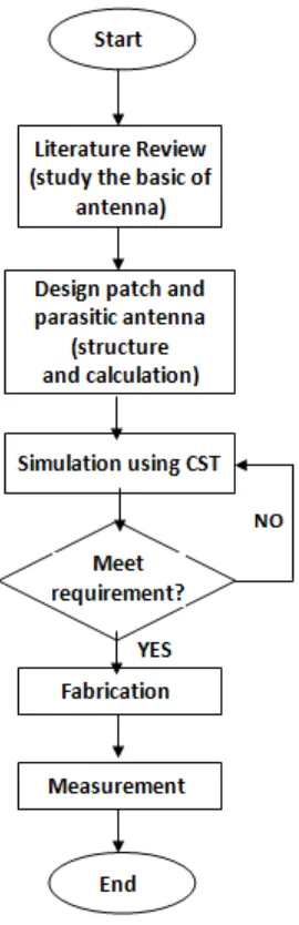
2.1 Flow Chart of Methodology 5
2.2 Radiation Pattern 7
2.3 Microstrip Patch Antenna 12
2.4 Typical Radiation Pattern of Rectagular Patch Antenna 14
2.5 Impedance Bandwidth Definition 16
2.6 Probe Feed Patch 18
2.7 Microstrip Line Feed Patch Antenna 18
2.8 Inset Line Microstrip Feed Patch Antenna 19
2.9 Aperture Coupled Patch Antenna 19
2.10 Cross Section of Aperture Coupled Patch Antenna 20 2.11 Microstrip Rectangular Patch Antenna Dimension 21 2.12 Microstrip Circular Patch Antenna Dimension 23 2.13 Rectangular Patch with the addition of parasitic ring 24 2.14 Broadband using rectangular patches parasitic elements 25
3.1 Parameters of Single Rectangular Patch Design 29
3.2 Parameters of Single Circular Patch Design 31
xvi
3.12 Circular Patch With Blade Curve Parasitic Element 2 42 3.13 Circular Patch with Blade Curve Parasitic Element 3 43 3.14 Circular Patch with Blade Curve Parasitic Element 4 44 3.15 Circular Patch with Ring Parasitic Element 1 45 3.16 Circular Patch with Ring Parasitic Element 2 46
3.17 CST Studio Suite 2009 48
3.18 The FR4 board that use in fabrication process. 48
3.19 Ultra Violet Ray Exposed Double Layer 49
3.20 Prototype of microstrip circular antenna 50
4.1 Microstrip circular with parasitic ring 53
4.2 simulated result of return loss for microstrip circular
with parasitic ring 53
4.3 Radiation pattern for for microstrip circular with parasitic ring 54 4.4 measured result of return loss for microstrip circular
with parasitic ring 54
4.5 Microstrip antenna with two blade curve parasitic elements 55 4.6 Simulation result of return loss for microstrip
antenna with two blade curve parasitic elements 55 4.7 Radiation pattern for microstrip antenna
with two blade curve parasitic elements 56
4.8 Measured result of return loss for microstrip antenna
with two blade curve parasitic elements 56
4.9 Microstrip antenna with 3 rectangular parasitic elements 57 4.10 Simulation result of return loss for microstrip
antenna with 3 rectangular parasitic elements 57 4.11 Radiation pattern for microstrip antenna with
3 rectangular parasitic elements 58
4.12 Measured result of return loss for microstrip
xvii
LIST OF ABBREVIATIONS
εr - Dielectric Constant ADS - Advance Design system
BW - Bandwidth
CST - Computer Software Technology
dB - Decibel
FNBW - First Null Beam Width
g2 - Height of the Ground
GPS - Global Positional System
h - Thickness of Substrate
HPBW - Half Power Beam Width
IEEE - Institute of Electrical and Electronics Engineers
RF - Radio Frequency
tan δ - Tangent Loss
CHAPTER 1
INTRODUCTION
This chapters covers the introduction of the project, background study regarding the project topic, project objective, the problem statement involves, the scope of work and the methodology of this project
1.1 Project Background
2
1.2 Project Objective
The objective of this project is to design a microstrip antenna with parasitic elements which can operate at frequency of 2.4 GHz and suitable gain.
1.3 Problem Statement
Microstrip antenna has a narrow bandwidth. Using only single antenna in the multi signal band is better than using the each antenna element in the separate way. Microstrip patch antennas are widely used because of there are many merits such as the low profile, light weight, low cast and planar also.
Microstrip antenna also has spurious feed radiation, poor polarization purity, limited power capacity, and tolerance problems.
However patch antenna have a disadvantage of narrow bandwidth typically 1-5 % impedance bandwidth, dielectric and conductor losses can be large for thin patches resulting in poor antenna efficiency and sensitivity to environmental factors such as temperature and humidity.
1.3 Scope of Work
3
1.4 Outlines of Thesis
CHAPTER 2
LITERATURE REVIEW
This chapter is discusses precisely about the information and theory relates to this project also the overview of major component involved. Factors that should be consider while developing this project also will be covered.
2.1 Project Flow
Following the project flow from the chapter 1, this project is start with studying the literature review about parameters of antenna such as matched impedance, VSWR, gain, frequency, bandwidth, return loss, amplitude of radiation pattern and polarization. These parameters determine the performance of the antenna designed.
Then the structure and dimension of the design is calculated to get the actual value in design part. For this project, there is a method that call parametric study or parametric sweep to get the value of the dimension.
5
Figure 2.1 : flow chart of methodology
It is followed by simulation running by Computer Simulation Technology (CST) Software to simulate the results of radiation pattern, return loss, directivity, gain, HPBW and FNBW.
6
The process of fabrication will take place where the actual dimension of the antenna is fabricated on the FR4 microstrip board. Etching process is done to perform the fabrication on the FR4 microstrip board.
The process of antenna measurement is where the experiment determines all the parameters above. Comparison and analysis of the fabricated and simulated design is made in order to verify the performance. The parameters of the antenna such as S-parameter, bandwidth and frequency can be tested by using network analyzer.
2.2 Introduction of Antenna
An antenna or aerial is a transducer designed to transmit or receive electromagnetic waves. In other words, antennas convert electromagnetic radiation into electrical current, or vice versa. Antennas generally deal in the transmission and reception of radio waves, and are a necessary part of all radio equipment. Antennas are used in systems such as radio and television broadcasting, point-to-point radio communication, wireless LAN, cell phones, radar, and spacecraft communication. Antennas are most commonly employed in air or outer space, but can also be operated under water or even through soil and rock at certain frequencies for short distances [1].
2.3 Antenna Parameters
2.3.1 Radiation Patterns
7
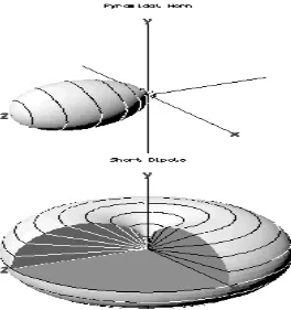
[image:24.595.183.447.238.519.2]In most cases, radiation pattern can be said as representation of the radiation properties of the antenna as a function of angular position. In term of angular position, there is power pattern which is the trace of angular variation of the received or radiated power at the constant radius from antenna. Amplitude field pattern is the trace of a spatial variation of the magnitude of magnetic field at a constant radius from the antenna. Often the field and power pattern are normalized with respect to their maximum value, yielding normalized field and power patterns.
Figure 2.2: Radiation Pattern