Australian Journal of Basic and Applied Sciences
ISSN:1991-8178Journal home page: www.ajbasweb.com
Corresponding Author: M. Idzdihar Idris, Faculty of Electronics and Computer Engineering, Universiti Teknikal Malaysia Melaka.
Thickness Dependence of The Surface Roughness of Micro Contact Deposited By Dc
Magnetron Sputtering Technique
1M. Idzdihar Idris, 2Nowshad Amin, 3Puvaneswaran Chelvanathan and 1Faiz Arith
1Faculty of Electronics and Computer Engineering, Universiti Teknikal Malaysia Melaka.
2Solar Energy Research Institute, Universiti Kebangsaan Malaysia, UKM, Bangi 43600, Selangor, Malaysia. 3
Department of Electrical, Electronic & System Engineering, Faculty of Engineering and Built Environment, Universiti Kebangsaan Malaysia, Bangi 43600, Selangor, Malaysia.
Background: Integrated circuits are tested in final step of IC packaging to verify that required electrical connections are working properly. At present, Pogo Pins are used as electrical connection between IC lead and load board. Pogo pins caused different problems including indentation marks, blur marks, tilting, spring malfunction, high maintenance cost and etc. The present miniaturization trends towards higher performance, smaller and lighter product have resulted in an increasing demand for smaller pitch size and increase the issues of testing process with pogo pins. Pogo pins induced reliability problems when dealing with fine-pitch (< 0.5 mm) packages. New electrical conductive cell was designed in previous works. It was based on micro-structures instead of pogo pins and consists of three different parts including polymer, metallic micro contactors and liquid metal. New Model was designed for QFP packages with 0.5 mm pitch size using simulation in previous years. Novel test socket mechanical design and analysis were successfully done by previous study. New models with new materials in different shapes were designed and the best one was achieved. background about topic of paper. Objective: This paper presents the influence of thickness on structural and surface roughness of micro contact probe cell for IC testing deposited by dc sputtering technique on a glass substrate.the main objective for your paper. Results: Micro contact with thickness of 2800-7000nm were deposited from Cu target at sputtering power of 125W in argon ambient gas at a room temperature on a base layer of copper using mask. The deposition conditions such as deposition rate, temperature and base pressure were fixed while, the deposition parameters (deposition times) were varied to obtain 4 different samples. The structural and surface roughness of micro contacts were investigated by using profilometer, scanning electron microscopy (SEM) and Atomic Force Microscopy (AFM). Conclusion: Results show that the micro contacts were successfully growth on a base layer of copper and the root mean square (RMS) roughness of micro contact was less than 25nm, 80nm and 100nm for window area of 1 x 1um2,, 5 x 5um2 and 10 x 10um2 respectively.. The interrelationship of grain growth and micro contact thickness are discussed in this paper.
© 2014 AENSI Publisher All rights reserved. To Cite This Article: M. Idzdihar Idris, Nowshad Amin, Puvaneswaran Chelvanathan and Faiz Arith., Thickness Dependence of The Surface Roughness of Micro Contact Deposited By Dc Magnetron Sputtering Technique. Aust. J. Basic & Appl. Sci., 8(6): 91-95, 2014
INTRODUCTION
IC testing is the final stage of semiconductor manufacturing process. It is so crucial and to ensure components delivered to customers can perform with excellent performance. In order to do IC testing, the device under test (DUT) is connected to a DUT board using a contactor and the DUT board is coupled to a testing machine. In these past few years, the spring- loaded probes, also known as pogo pins, are used as electrical connection between IC leads and load board. Pogo pins are housed in sockets and formed in an array to simultaneously provide contact between the DUT and the DUT board. Pogo pin is a conductive material that provides an electrical connection between the DUT and DUT board.
Therefore, a new design that induces no puncture marks on the DUT contact leads is required. Design and
development of a test fixture for semiconductor final testing was introduced byusing ANSYS as Finite Element
Analysis (FEA) software (N. Amin, 2009). Proposed electrical conductive cells utilize a combination of three different kinds of materials such as polymer, metallic and liquid metal. Liquid metal is used to absorb the
pressure and prevent damaging to the IC leads (Z. Ehtiatkha, 2011). From the simulation result, the best
parameters of micro contact were obtained. In the previous research work, the deposition of the micro contact by DC magnetron sputtering technique was analyzed and micro contact columns were successfully formed (M. Idzdihar, 2014).
This paper presents the relation of surface roughness and thickness of micro contacts fabricated by DC Magnetron Sputtering technique.
MATERIALS AND METHODS
All micro contacts were deposited with a dc magnetron sputtering system using a circular 5.08cm diameter
Cu target of 99.995% purity. The target to substrate distance was 9 cm. The substrates for the deposition were soda lime glass and were cleaned follow standard cleaning procedure. The base pressure was around 13 to 15
miliTorr, achieved with a cryo pump coupled with a rotary pump. The sputtering deposition was carried in high
purity argon (Ar) gas (99.999%) with dc sputtering power of 150 W, which led to a deposition rate of approximately 3 (A/sec). In order to study the influences of the film thickness, 4 samples of micro contact with
thicknesses controlled at around 130–1050 nm were fabricated at room temperature. The thicknesses of these Cu
films were checked with a quartz crystal monitor located near the substrate during the sputtering process, and was quantified with the surface profilometer after the deposition process by measuring the step height between masked and unmasked regions on the substrate. The surface morphology and microstructure of the films were examined by means of surface electron microscopy (SEM) and atomic force microscopy (AFM). In particular,
the root mean square (RMS) roughness was evaluated by using AFM image area of 1 um2. The deposition
conditions of the micro contact column on base layer of copper presented in this work are summarized in Table 1. The variable parameter for the micro contact deposition is the deposition time for each sample where sample A1 was deposited in 1 hour, sample A2 in 2 hours, sample A3 for 3 hours and sample A4 for 4 hours.
Table 1: Deposition parameters for the micro contact column.
Target Cu
Surface structure and roughness of micro contact column (circle area):
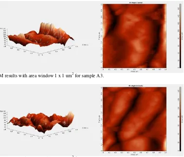
The most common application of Atomic Force Microscopy (AFM) is to get the surface structure or morphology of deposited sample in high resolution image and characterize its surface roughness. It is important to know the surface feature as it imply the quality of the deposited samples. Since all the parameters for each sample are the same except for the deposition time, the variation of the surface characteristic might response to the thickness of micro contact. The AFM results illustrating the 3-D and 2-D surface structure of micro contact column (circle area) in window area of 1 um x 1 um is shown in Figure 1 to Figure 1 for sample A1, A2, A3 and A4, respectively. In these micrographs, grain features protruding from the film surface develop in the copper films. It was observed that the grains have agglomerated together and formed smaller number of big grains.
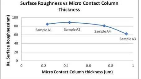
Based on data from profilometer (M. Idzdihar, 2014) and result from AFM, the surface roughness of micro contact column for sample A1, A2, A3 and A4 are correlated with the micro contact column thickness as in
Figure 5, Figure 6, and Figure 7 for window area of 1 x 1um2,, 5 x 5um2 and 10 x 10um2 respectively. As a
whole, the surface roughnesses of the micro contact columns are not exceeding 100 nm which is showing that the samples have a good quality. In window area of 1 x 1um2, the surface roughness of each micro contact column is below than 25 nm. While in window area of 5 x 5um2and 10 x 10um2,it showed that sample A3 (micro contact height = 0.94um) has the lowest surface roughness. This may happen because sample A3 has a very low shadow effect and longtime of deposition where the atoms bombarded have more time to rearrange themselves and settle down at the opening circle to form a well shape column of micro contact. It can be concluded that to get a good quality of micro contact in term of surface roughness, the shadow effect and micro
Fig. 1: AFM results with area window 1 x 1 um2 for sample A1.
Fig. 2: AFM results with area window 1 x 1 um2 for sample A2.
Fig. 3: AFM results with area window 1 x 1 um2 for sample A3.
Fig. 5: Correlation between surface roughness and micro contact column thickness with area window 1 x 1 um2
Fig. 6: Correlation between surface roughness and micro contact column thickness with area window 5 x 5 um2
Fig. 7: Correlation between surface roughness and micro contact column thickness with area window 10 x 10 um2
Conclusion:
The thickness dependence of the structural and surface roughness of the micro contact deposited by DC magnetron sputtering technique has been presented in this paper. The surface morphological study with SEM generally shows the growth of micro contact on base layer, while the AFM results reveal that the surface
roughness’s of the micro contact columns are not exceeding 25 nm which show that the samples have a good
quality All the obtained results show the potential viability to solve the limitation of the pogo pin based testing tools by replacing them with the new novel IC test fixture as demonstrated in this study.
REFERENCES
Amin, N., H.W. Koay, Z.Y. Lam, 2009. "Semiconductor final test fixture design with microstructure alloy contacts using Finite Element Analysis," in Electronics Packaging Technology Conference, 2009. EPTC '09. 11th, pp: 834-837.
Amin, N., Z.Y. Lam, 2008. “A Practical Investigation on the Root Causes of the Mechanical Damages of
Ehtiatkha, Z., S. Basiri, N. Amin, 2011. “Mechanical Design and Analysis of Innovative Integrated Circuit
Test Socket”, RSMC 2011 Proc., pp: 65-69.
Idzdihar Idris, M., Nowshad Amin, Faiz Arith, S.A.M. Chachuli, 2014. “Deposition of micro Contact Based
Probe Cell for IC Testing by DC Magnetron Sputtering Technique”, Res. J. Appl. Sci. Eng. & Tech., 7(13):
2040-7459.
Teng, H.C., M.K. Chen, C.H. Yeh, Y.J. Huang, S.L. Fu, 2007. “Study of Contact Degradation in Final