STAND-ALONE DATA LOGGER SYSTEM
OOI KIN YEW
This report is submitted in partial fulfillment of the requirements for the award of Bachelor of Electronic Engineering (Computer Engineering) With Honours
Faculty of Electronic and Computer Engineering Universiti Teknikal Malaysia Melaka
UNIVERSTI TEKNIKAL MALAYSIA MELAKA
FAKULTI KEJURUTERAAN ELEKTRONIK DAN KEJURUTERAAN KOMPUTER
BORANG PENGESAHAN STATUS LAPORAN PROJEK SARJANA MUDA II
Tajuk Projek : Stand-Alone Data Logger System
Sesi
Pengajian : 2 / 2008/2009
Saya ………OOI KIN YEW @ WONG KIN YEW………
(HURUF BESAR)
mengaku membenarkan Laporan Projek Sarjana Muda ini disimpan di Perpustakaan dengan syarat-syarat kegunaan seperti berikut:
1. Laporan adalah hakmilik Universiti Teknikal Malaysia Melaka.
2. Perpustakaan dibenarkan membuat salinan untuk tujuan pengajian sahaja.
3. Perpustakaan dibenarkan membuat salinan laporan ini sebagai bahan pertukaran antara
institusi pengajian tinggi.
4. Sila tandakan ( √ ) :
SULIT*
(Mengandungi maklumat yang berdarjah keselamatan atau kepentingan Malaysia seperti yang termaktub di dalam AKTA RAHSIA RASMI 1972)
TERHAD* (Mengandungi maklumat terhad yang telah ditentukan oleh
organisasi/badan di mana penyelidikan dijalankan)
TIDAK TERHAD
Disahkan oleh:
__________________________ ___________________________________
(TANDATANGAN PENULIS) (COP DAN TANDATANGAN PENYELIA)
Alamat Tetap: 12, REGAT TASEK TIMUR 20,
TAMAN RIA, 31400 IPOH, PERAK.
DECLARATIONS
“I hereby declare that this report is the result of my own work except for quotes as cited in the references.”
“I hereby declare that I have read this report and in my opinion this report is sufficient in terms of the scope and quality for the award of Bachelor of Electronic
Engineering (Computer Engineering) With Honours”.
Signature : ………..
Supervisor’s Name : ………..
ACKNOWLEDGEMENT
First and foremost, I would like to extend my appreciation to all who contributed time, concern and efforts to lend a helping hand and thus allow me to gain invaluable knowledge. On top of that, I would like to reserve a special thank to my supervisor, Mr. David Yap for his excellent mentoring and guidance. All his comments and constructive criticism played a pivotal role throughout my project development.
ABSTRACT
ABSTRAK
TABLE OF CONTENTS
CHAPTER CONTENT PAGE
PROJECT TITLE i
DECLARATIONS iii
DEDICATION v
ACKNOWLEDGEMENT vi
ABSTRACT vii
ABSTRAK viii
TABLE OF CONTENTS ix
LIST OF TABLES xi
LIST OF FIGURES xii
LIST OF ABBREVIATIONS xiv
LIST OF APPENDIX xv
I INTRODUCTION
1.1 Overview 1
1.2 Objectives 2
1.3 Problem Statement 2
1.4 Scope 3
1.5 Project Methodology 3
1.6 Report Structure 4
II LITERATURE REVIEW
2.1 Theory
2.1.2 Microcontroller PIC16F877A 7 2.1.3 Microcontroller PIC18F452 13
2.1.4 RS232 Serial Port 15
2.1.5 SD/MMC Card 18
2.1.6 MikroC Compiler 23
2.2 Case Study
2.5.1 Case Study 1
Microcontroller Based Data Logger System 25 2.5.2 Case Study 2
HWS Data Logger System 26
III PROJECT METHODOLOGY
3.1 Project Methodology 28
3.1.1 Hardware Development 30
3.1.2 Software Development 37
3.1.2.1 LED Blinking Simulation 39
IV RESULT
4.1 Result
4.1.1 ADC Converter 41
4.1.2 SD/MMC Initialization and Data Writing 43 4.1.3 Hardware Fabrication and Circuit Testing 45
4.1.4 Discussion 48
V CONCLUSION
5.1 Conclusion 49
5.2 Future Work 49
LIST OF TABLES
NO TITLE PAGE
2.1 PIC16877A Key Features 8
2.2 Operation of each PIC16F877A pin 10
2.3 PIC18F452 Key Features 13
2.4 Function of connector 1 & 2 handshaking 17
2.5 SD Memory card pad/pin assignments 22
2.6 SD Memory card registers 23
LIST OF FIGURES
NO TITLE PAGE
1.1 A general flowchart of the project 3
2.1 Datasheet of PIC16F877A 7
2.2 PIC16F877 Block Diagram 9
2.3 PIC16F877A Special Function Register 12
2.4 PIC18F452 Block Diagram 14
2.5 PIC18F452 Special Function Register 15
2.6 RS232 DB9 to DB25 converter 16
2.7 RS232 DB9 Pinout 16
2.8 DB9 Mating Connection 17
2.9 SD Mode Communication 19
2.10 SPI Mode Communication 20
2.11 Slave Select (SS) SPI Interface 21
2.12 Full Duplex Slave Select (SS) SPI Interface 21
2.13 Memory card shape and interface 22
2.14 General layout of a mikroC window 24
2.15 Architecture of the Microcontroller based Data Logger System 25 2.16 HWS Data Logger System hardware (Logger and Reader) 26 2.17 The software flowchart and handshaking of HWS Host Software 27
3.1 General Block Diagram of Project 28
3.2 Flowchart of Literature Review 29
3.3 Flowchart of Hardware Development 30
3.4 ISKIM PIC Kit 31
3.5 The circuit diagram of the ISKIM PIC kit 31
3.7 Input Interface Circuit 33
3.8 LCD to ISKIM PIC kit 33
3.9 SD/MMC Prototype Board 34
3.10 The circuit diagram of the SD/MMC Prototype Board 34
3.11 SD/MMC Interface Circuit 35
3.12 Complete circuitry 36
3.13 Circuit to casing installation 36
3.14 Exterior outlook 37
3.15 Flowchart Software Development 38
3.16 PIC Bootloader 40
3.17 The LED Blinking Result 40
4.1 ADC circuit simulation 42
4.2 The output after ADC conversion 42
4.3 Proteus Simulation 44
4.4 Data written in file “SIGNALA.txt” 44
4.5 LCD start-up display 45
4.6 MMC/SD Detection/Initialized 46
LIST OF ABBREVIATIONS
SD - Secure Digital
MMC - MultiMediaCard
PIC - Peripheral Interface Controller CPU - Central Processing Unit DIP - Dual Inline Package
IC - Integrated Chip
EEPROM - Electrically Erasable Programmable Read-Only Memory
PWM - Pulse Width Modulation
USART - Universal Asynchronous Receiver/Transmitter MSSP - Master Synchronous Serial Port
I/O - Input/output
SPI - System Packet Interface
CLK - Clock
SCLK/SCK - Serial Clock
CMD - Command
CS - Chip Select
MOSI - Master Out Slave In MISO - Master In Slave Out
ANSI - American National Standards Institute IDE - Integrated Drive Electronics
LIST OF APPENDIX
NO TITLE PAGE
A1 Adc converter source code 52
A2 Data storage source code 53
B1 Datasheet PIC16F877 (ADC Converter) 54
CHAPTER I
INTRODUCTION
This project is mainly centered on a design of a stand-alone data logger system which is capable to acquire, record and store data / input signal from the function generator for monitoring purposes. This design utilizes both the PIC and memory card capabilities. The data stored will then be monitored using computer. The whole concept would indefinitely simplify the convenience of data logging.
1.1 OVERVIEW
Memory Card to a computer through the computer interface. The computer then analyzes the data.
Data loggers are employed in many industries to ascertain various environmental parameters. Generally, this project is intended to provide a suitable interfacing system between the signals from the function generator to the PIC microcontroller and subsequently stores the data into a memory card for future analysis.
1.2 OBJECTIVES
The objective of this project is to develop a stand-alone data logger system for voltage signals obtained from the function generator. The objectives can be summarized as below:
a) To use PIC to acquire and record the data
b) To transmit the acquired data to a SD/MMC card via Serial Peripheral Interface (SPI mode)
c) To store the PIC data using a memory card
1.3 PROBLEM STATEMENT
1.4 SCOPE
a) Research study on the on the Programmable Intelligence Computer, PIC18F452 microcontroller and the control system of the circuit.
b) To acquire the function generator signal for data logging. c) To develop a PIC to memory card interface.
d) To design an ideal circuit simulation using suitable computer language and software to enable data transmission to the memory card and test its efficiency.
e) To construct and develop the model of the circuit designed (hardware)
1.5 PROJECT METHODOLOGY
a) Project Planning b) Literature Review c) Data Collection
d) Software Design & Circuit Construction for the acquisition of data e) PIC interfacing to transfer signal to memory card
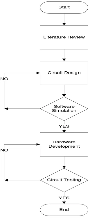
Start
Literature Review
Circuit Design
Software Simulation
Hardware Development
Circuit Testing
End YES
YES NO
[image:19.595.264.419.69.445.2]NO
Figure 1.1: A general flowchart of the project
1.6 REPORT STRUCTURE
Chapter I briefly introduces the general overview of the Stand-alone Data Logger project. The introduction consists of overview, objective, problem statement, scope of work, methodology and report structure.
Chapter III explains about the project methodology. Project methodology gives comprehensive details about the method used to solve problem to complete the project. This chapter touches on the methods used for data collection, software and circuit design, PIC interfacing, SD/MMC memory card interfacing and performance analysis with the aid of block diagrams and flowcharts.
Chapter IV consists of result and discussion to overall result, finding and analysis throughout the research and project development. It inevitably shows how precise the hypothesis could be to realization.
CHAPTER II
LITERATURE REVIEW
2.1 THEORY
In this chapter, the focus is on the literature review conducted on a wide range of correlated studies necessary to complete this project. This includes the Peripheral Interface Controller (PIC) microcontroller or precisely the PIC16F877A and PIC18F452 microcontrollers, RS232 Serial Port, SD/MMC Card and its interface and mikroC, the software chosen to be applied in this project.
2.1.1 PERIPHERAL INTERFACE CONTROLLER (PIC)
PIC (Peripheral Interface Controller) is a family of Harvard architecture microcontrollers. It is an IC developed to control peripheral devices, to ease the load from the main CPU. The PIC, akin to the CPU, has calculation functions and memory, and is controlled by the software. It has separate code and data spaces in accordance to Harvard architecture [1].
The characteristics of a general PIC architecture are: f) A small number of fixed length instructions.
h) A single accumulator (W), the use of which (as source operand) is implied.
i) All RAM locations function as registers as both source and/or destination of math and other functions.
j) A hardware stack for storing return addresses.
k) A fairly small amount of addressable data space (typically 256 bytes), extended through banking.
l) Data space mapped CPU, port, and peripheral registers.
m) The program counter is also mapped into the data space and writable (this is used to synthesize indirect jumps).
[image:22.595.211.431.359.604.2]2.1.2 MICROCONTROLLER PIC16F877A
Figure 2.1: Datasheet of PIC16F877A [3]
Table 2.1: PIC16877A Key Features [3]
Key Features PIC16F877A
Operating Frequency DC - 20 MHz
RESET (and Delays) POR, BOR
(PWRT, OST)
FLASH Program Memory (14-bit words)
8K
Data Memory (bytes) 368
EEPROM Data Memory 256
Interrupts 14
I/O Ports Ports A,B,C,D,E
Timers 3
Capture/Compare/PWM Modules 2
Serial Communications MSSP, USART
Parallel Communications PSP
10-bit Digital-to-Analog Module 8 input channels
![Figure 2.1: Datasheet of PIC16F877A [3]](https://thumb-ap.123doks.com/thumbv2/123dok/640868.77898/22.595.211.431.359.604/figure-datasheet-of-pic-f-a.webp)
![Table 2.1: PIC16877A Key Features [3]](https://thumb-ap.123doks.com/thumbv2/123dok/640868.77898/23.595.170.470.107.600/table-pic-a-key-features.webp)
![Figure 2.2: PIC16F877 Block Diagram [3]](https://thumb-ap.123doks.com/thumbv2/123dok/640868.77898/24.595.121.520.69.555/figure-pic-f-block-diagram.webp)
