IEEE ELECTRON DEVICE LETTERS, VOL. 30, NO. 10, OCTOBER 2009 1039
Pentacene-Based Thin-Film Transistors With a
Solution-Process Hafnium Oxide Insulator
Chia-Yu Wei, Feri Adriyanto, Yu-Ju Lin, Yu-Chang Li, Tong-Jyun Huang,
Dei-Wei Chou, and Yeong-Her Wang,
Member, IEEE
Abstract—Pentacene-based organic thin-film transistors with solution-process hafnium oxide (HfOx) as gate insulating layer
have been demonstrated. The solution-process HfOx could not
only exhibit a high-permittivity(κ=11)dielectric constant but also has good dielectric strength. Moreover, the root-mean-square surface roughness and surface energy(γs)on the surface of the
HfOx layer were 1.304 nm and 34.24 mJ/cm2, respectively. The
smooth, as well as hydrophobic, surface of HfOx could facilitate
the direct deposition of the pentacene film without an additional polymer treatment layer, leading to a high field-effect mobility of 3.8 cm2/(V
·s).
Index Terms—Hafnium oxide, high permittivity, organic thin-film transistor (OTFT), solution process, surface energy.
I. INTRODUCTION
O
RGANIC thin-film transistors (OTFTs) have drawn ex-tensive attention for their applications in radio-frequency rectifiers, chemical sensors, and integrated circuits. The char-acteristics of pentacene-based thin-film transistors with a mo-bility of 1.5 cm2/(V·s) have been reported [1]. They were found to approach the level of hydrogenated amorphous silicon (a-Si:H) TFTs [2]. However, a reduction of operating voltage for OTFTs can be achieved through increasing capacitance density by using a high-permittivity inorganic metal–oxide gate insulator or by reducing the thickness of the gate insulator. In addition, typical high-κinorganic metal–oxide gate insulators cannot only be thick to prevent serious gate leakage current but also maintain the same level of capacitance density.
A number of high-permittivity inorganic metal–oxide materi-als, such as tantalum oxide [3], titanium oxide [4], magnesium
Manuscript received June 22, 2009; revised July 25, 2009. First published September 1, 2009; current version published September 29, 2009. This work was supported in part by the National Science Council of Taiwan under Contract NSC 95-2221-E-006-428-MY3. The review of this letter was arranged by Editor A. Nathan.
C.-Y. Wei is with the Institute of Electro-Optical Science and Engineering, National Cheng Kung University, Tainan 701, Taiwan (e-mail: l7896118@mail. ncku.edu.tw).
F. Adriyanto, Y.-J. Lin, Y.-C. Li, and T.-J. Huang are with the Institute of Microelectronics, Department of Electrical Engineering, National Cheng Kung University, Tainan 701, Taiwan (e-mail: [email protected]; yjlin@ mail.ncku.edu.tw; [email protected]; [email protected]). D.-W. Chou is with the Department of Aviation and Communica-tion, Air Force Institute of Technology, Kaohsiung 820, Taiwan (e-mail: [email protected]).
Y.-H. Wang is with the Institute of Microelectronics, Department of Electri-cal Engineering, National Cheng Kung University, Tainan 701, Taiwan, and also with the National Applied Research Laboratory, Taipei 106, Taiwan (e-mail: [email protected]).
Color versions of one or more of the figures in this letter are available online at http://ieeexplore.ieee.org.
Digital Object Identifier 10.1109/LED.2009.2029876
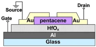
Fig. 1. Cross-sectional schematics of the pentacene-based TFTs. The thick-ness of HfOxwas 190 nm, which was measured by the Alpha step.
oxide [5], and hafnium oxide [6], have been widely studied. Among these different materials, hafnium oxide is a promising candidate due to its larger bandgap than other high-permittivity competitors [7]. However, most high-permittivity inorganic metal–oxide films have been deposited by sputtering [3], [4] or electron-beam evaporation [6] under a vacuum system. In addition, most high-κmaterials are based on ceramics, which are fragile and are not suitable for flexible and large-area elec-tronics [8]. In this letter, the solution-processed HfOxfilm will be demonstrated by spin coating under a low-cost deposition system. The simple transistor structure, good performance, and the absence of any surface treatments would be applicable for large-area or ink-jet electronic technology. The corresponding physical and electrical properties of the HfOx as the gate insulating layer of OTFTs will be investigated.
II. DEVICESTRUCTURE ANDFABRICATION
The cross-sectional schematic of top contact pentacene-based TFTs is shown in Fig. 1. Aluminum (Al) was deposited by RF sputtering through a shadow mask to form the gate elec-trode on the Corning glass Eagle2000substrate. Hafnium oxide solution was prepared by mixing 4.96-g hafnium dichloride oxide octahydrate, 98+%(40 wt% from Alfa Aesar) with 1-g glycine (8 wt%), and 3.6 ml of deionized (DI) water; then, it was boiled to dissolve the solutes under the airtight space. Subsequently, the limpid solution at room temperature was done by adding 2.95-ml DI water and then spin coated onto the Al/glass substrate to form a transparent insulating layer. Finally, the sample was baked on a hot plate at 200 ◦C for 30 min under ambient air condition, and the thickness of the gate insulating layer was 190 nm, as determined by an Alpha-step surface profiler. Pentacene was thermally evaporated on the insulating layer at a deposition rate of 0.08 nm/s. The gold electrode patterns were finally deposited by RF sputtering as the source and drain, and the channel length(L)and width(W)
were 150 and 1500µm, respectively.
1040 IEEE ELECTRON DEVICE LETTERS, VOL. 30, NO. 10, OCTOBER 2009
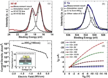
Fig. 2. XPS core level spectra of (a) Hf 4fand (b) O 1semissions from the HfOxthin film cured at 200◦C for 30 min under ambient air condition. (c) Leakage
current density versus applied electric field (J–E) and capacitance density versus applied voltage (C–V) characteristics were plotted from the metal–oxide–metal
(Al−HfOx−Au)structure. (d) Current–voltage characteristics (ID–VD) for a pentacene-based OTFT with a 190-nm-thick HfOxinsulator.
The electrical characteristics of the transistor were measured by the semiconductor parameter analyzer HP 4156B under atmospheric condition at room temperature. The chemical com-position and binding energy of the HfOxfilm were analyzed by X-ray photoelectron spectroscopy (XPS).
III. IMPLEMENTATION ANDPERFORMANCE
Fig. 2 shows the Hf4f and O1semission spectra from the spin-coated HfOxlayer. Fig. 2(a) shows the doublet feature in the range between 16 and 20 eV, which is spin splitting of 16.87 and 18.6 eV. Such phenomena may be due to the splitting of Hf
4f 7/2 and 5/2 spin states and indicates the formation of energy of the Hf–O bonds. In addition, the theoretical value of the O1speak binding energy from HfO2is 530.4 eV [9]. The other chemical state of O1sat 531.8 eV from our sample, as shown in Fig. 2(b), is probably due to the moisture and hydroxyl groups under the atmosphere environment [10]. A good agreement between the simulation results composed of two different O1s
states with the measurement data can be observed. By using the XPS data, the ratio between O and Hf with a value ofx=4.58 can be obtained.
Fig. 2(c) shows the leakage current density(JL)as a function of the applied electrical field of the metal–insulator–metal
(Al−HfOx−Au)structure. The capacitance of the HfOxlayer was measured through HP 4280A measurement under 1 MHz, as shown in the inset of Fig. 2(c). According to the capacitance data, the dielectric constantκwas estimated to be about 11.16. As compared to other processes, the lower value of the dielec-tric constant may be attributed to the loose structure that has a lot of moisture during the solution process. However, the leak-age current density of the spun HfOxwith a dielectric strength
of 4.36×10⁻⁶ A/cm2 at an electric field of−2 MV/cm can be seen. The leakage current density is still high and needs further improvement. The integrity of looser solution-processed dielectrics can be improved by annealing at higher temperature to make the device reliable.
Fig. 2(d) shows the current–voltage characteristics at differ-ent gate–source voltages(VG)from 0 to−15 V for pentacene-based OTFTs with a HfOx single-layer gate insulator. When the VG is biased at−12.5 V, an output drain current (ID)of −15 µA can be obtained. In addition, the threshold voltage
(VT) is−7.46 V. The on/off current ratio is about 102 from −15 and 0 V of gate bias at VDS=−10 V [11]. This low value may partly be attributed to the loose dielectric structure by the solution process. A subthreshold slope swing (SS) of 2.6 V/dec is obtained. The linear field-effect mobility is about 0.6 cm2/(V
·s). According to a published paper [12], the field-effect mobility could be calculated at the saturation region with a capacitance of 52 nF/cm2. A saturation field-effect mobility of 3.8 cm2/(V
·s)is obtained when theVGis biased at−10 V in the saturation region. Several published reports [5], [13] have indicated that the saturation mobility of pentacene film could be improved by the smoother surface roughness or the more hydrophobic surface of the insulator through treatment modification. In this letter, the smooth root-mean-square (rms) surface roughness and matching surface free energy of the HfOx layer could contribute to the superior saturation mo-bility without an additional treatment process, as discussed hereinafter.
WEIet al.: THIN-FILM TRANSISTORS WITH A SOLUTION-PROCESS HAFNIUM OXIDE INSULATOR 1041
TABLE I
COMPARISON OF THEPUBLISHEDHIGH-κMATERIALSWITHTHAT OFTHISLETTER
Owens and Wendt [14], the surface energy of the HfOx layer can be written as
l are the dispersion and polar terms of the liq-uid surface energy, which are 21.8 and 51.8 mJ/m2for DI water while 50.8 and 0 mJ/m2for di-iodomethane, respectively.γ
lis the total surface energy of the liquid, which can be obtained by adding the dispersion and polar terms. The surface energy of the HfOx layer can be solved from (1) through the linear equation in two variables. Finally, the total surface energy of the inorganic HfOxlayer is 34.24 mJ/m2. According to the work of Drummy and Martin [15], the surface energy theoretical value derived for the orthorhombic-phase pentacene grown was 38 mJ/m2. This result is compatible with the polymer ad-ditional treatment layers, such as 39.7 mJ/m2 of poly(imide siloxane) [16] or 38.2 mJ/m2 of photosensitive polyimide [17]. Table I shows a comparison of the published high-κ
materials with that of this letter. According to the definition of on/off ratio [11], the OFF current state was extracted at
VGS=0 for comparison. The large threshold voltage and sub-threshold SS need further improvements. As to the surface roughness, effective saturation mobility, and dielectric strength, the proposed transistors are much better than those of the reported data.
IV. CONCLUSION
In summary, pentacene-based OTFTs with the solution-processed HfOx dielectric have been demonstrated. The solution-processed HfOxcould not only provide a high dielec-tric constant (κ=11) but also has good dielectric strength. Moreover, the rms surface roughness and surface energy(γs) on the surface of the HfOxlayer are 1.304 nm and 34.24 mJ/ cm2, respectively, which are compatible to those with additional treatments. The smooth and hydrophobic surface of HfOxcould facilitate the direct deposition of the pentacene film, leading to a high field-effect mobility of 3.8 cm2/(V
·s). Finally, this letter has shown the low-cost solution process for inorganic material insulators, making them applicable for pentacene-based TFTs.
REFERENCES
[1] C. D. Dimitrakopoulos and P. R. L. Malenfant, “Organic thin film tran-sistors for large area electronics,”Adv. Mater., vol. 14, no. 2, pp. 99–117, Jan. 2002.
[2] T. N. Jackson, Y. Y. Lin, D. J. Gundlach, and H. Klauk, “Organic thin-film transistors for organic light-emitting flat-panel display backplanes,”
IEEE J. Sel. Topics Quantum Electron., vol. 4, no. 1, pp. 100–104, Jan./Feb. 1998.
[3] Y. Zhao, G. Dong, L. Wang, and Y. Qiu, “Improved photostability of organic thin film transistors with tantalum oxide–poly(4-vinylphenol) double gate insulators,”Appl. Phys. Lett., vol. 90, no. 25, p. 252 110, Jun. 2007.
[4] K. Choi, D. K. Hwang, K. Lee, J. H. Kim, and S. Im, “Pentacene thin-film transistors with polymer/TiOxdouble-layer dielectrics operating at 3 V,” Electrochem. Solid-State Lett., vol. 10, no. 3, pp. H114–H116, Jan. 2007. [5] S. S. Cheng, C. Y. Yang, C. W. Ou, Y. C. Chuang, M. C. Wu, and C. W. Chu, “Pentacene thin-film transistor with PVP-capped high-kMgO dielectric grown by reactive evaporation,”Electrochem. Solid-State Lett., vol. 11, no. 5, pp. H118–H120, Feb. 2008.
[6] P. T. Liu, Y. M. Chou, and P. Y. Yang, “Dielectric hafnium oxide improved by supercritical carbon dioxide fluid treatment for pentacene thin-film transistors,” Electrochem. Solid-State Lett., vol. 11, no. 7, pp. H165– H168, Apr. 2008.
[7] G. D. Wilk, R. M. Wallace, and J. M. Anthony, “High-κgate dielectrics: Current status and materials properties considerations,”J. Appl. Phys., vol. 89, no. 10, pp. 5243–5275, May 2001.
[8] F. C. Chen, C. W. Chu, J. He, Y. Yang, and J. L. Lin, “Organic thin-film transistors with nanocomposite dielectric gate insulator,”Appl. Phys. Lett., vol. 85, no. 15, pp. 3295–3297, Oct. 2004.
[9] P. D. Kirsch, C. S. Kang, J. Lozano, J. C. Lee, and J. G. Ekerdt, “Electrical and spectroscopic comparison of HfO2/Si interfaces on nitrided and un-nitrided Si(100),”J. Appl. Phys., vol. 91, no. 7, pp. 4353–4363, Apr. 2002. [10] T. L. Barr, “ESCA studies of naturally passivated metal foils,”J. Vac. Sci.
Technol., vol. 14, no. 1, pp. 660–665, Jan./Feb. 1977.
[11] D. R. Gamota, P. Brazis, K. Kalyanasundaram, and J. Zhang,Printed Organic and Molecular Electronics. Norwell, MA: Kluwer, 2004, ch. 4, sec. 1, pp. 364–365.
[12] Y. J. Lin, Y. C. Li, C. C. Yeh, S. F. Chung, L. M. Huang, T. C. Wen, and Y. H. Wang, “Organic thin film transistor by using polymer electrolyte to modulate the conductivity of conjugated polymer,”Appl. Phys. Lett., vol. 89, no. 22, p. 223 518, Dec. 2006.
[13] P. Kim, X. H. Zhang, B. Domercq, S. C. Jones, P. J. Hotchkiss, S. R. Marder, B. Kippelen, and J. W. Perry, “Solution-processible high-permittivity nanocomposite gate insulators for organic field-effect transis-tors,”Appl. Phys. Lett., vol. 93, no. 1, p. 013 302, Jul. 2008.
[14] D. K. Owens and R. C. Wendt, “Estimation of the surface free energy of polymers,”J. Appl. Polym. Sci., vol. 13, no. 8, pp. 1741–1747, Aug. 1969. [15] L. F. Drummy and D. C. Martin, “Thickness-driven orthorhombic to tri-clinic phase transformation in pentacene thin films,”Adv. Mater., vol. 17, no. 7, pp. 903–907, Apr. 2005.
[16] S. Y. Yang, K. Shin, and C. E. Park, “The effect of gate-dielectric sur-face energy on pentacene morphology and organic field-effect transis-tor characteristics,”Adv. Funct. Mater., vol. 15, no. 11, pp. 1806–1814, Nov. 2005.