UNIVERSITI TEKNIKAL MALAYSIA MELAKA FACULTY OF ELECTRICAL ENGINEERING
PROJEK SARJANA MUDA II
BEKU 4983
WIRELESS POWER TRANSFER FOR CELL PHONE CHARGING APPLICATION
Soo Eng Kuan
Bachelor of Electrical Engineering (Control, Instrumentation and Automation)
“I hereby declare that I have read through this report entitle “Wireless Power Transfer For Cell Phone Charging Application” and found that it has comply the partial fulfilment for awarding the degree of Bachelor of Electrical Engineering (Control, Instrumentation & Automation)”
Signature :
Supervisor’s Name : MR. LIM WEE TECK
WIRELESS POWER TRANSFER FOR CELL PHONE CHARGING APPLICATION
SOO ENG KUAN
A report submitted in partial fulfilment of the requirements for the degree of Electrical Engineering (Control, Instrumentation & Automation)
Faculty of Electrical Engineering
UNIVERSITY TEKNIKAL MALAYSIA MELAKA
iii
I declare that this report entitle “Wireless Power Transfer for Cell Phone Charging Application” is the result of my own research except as cited in the references. The report
has not been accepted for any degree and is not concurrently submitted in candidature of any other degree.
Signature :
Name : SOO ENG KUAN
iv
DEDICATION
I dedicate this study to my family, especially…
to Father and Mother for instilling the importance of hard work and higher education;
to late grandmother, late grandfather for encouragement; to my sisters—may you also be motivated
v
ACKNOWLEDGEMENT
I would never have been able to finish my project without the guidance of my lecturers, help from friends, and support from my family members.
I would like to express my earnest gratitude to my supervisor, Mr. Lim Wee Teck for his tremendous guidance, patience, caring, and patiently corrected my writing; without his knowledge and assistance, this research would not have been successful.
I would like to thank Leong Yoke Theng, who provided me with some study material. Many thanks to Liew Phek Chia for sharing her research information throughout my preparation of this project.
vi
ABSTRACT
vii
ABSTRAK
viii
TABLE OF CONTENTS
CHAPTER TITLE PAGE
ACKNOWLEDGEMENT v
ABSTRACT vi
TABLE OF CONTENTS viii
LIST OF TABLES x
LIST OF FIGURES xi
LIST OF ABBRIVIATIONS AND SYMBOLS xiv
LIST OF APPENDIXES xv
1 INTRODUCTION 1
1.1. Introduction 1
1.2. Project Statement 1
1.3. Objectives 1
1.4. Scopes 2
2 LITERATUREREVIEW 3
2.1. Introduction 3
2.2. Theoretical Background 3
2.2.1. Rectifiers 6
2.2.2. Inverters 9
2.2.3. Faraday’s Law of Induction 12
2.2.4. Resonant Inductive Coupling 13
2.2.5. Multivibrators 15
2.2.6. Diode Rectifiers 18
2.3. Previous Works 20
ix
CHAPTER TITLE PAGE
3 METHODOLOGY 23
3.1. Introduction 23
3.2. Project Flow 23
3.3. Data Collection 25
3.4. Simulations 26
3.4.1. AC-DC Converter with Transformer 26 3.4.2. Transformerless AC-DC Converter 28
3.4.3. 555 Timer in Astable Operation 30
3.4.4. Diode Rectifiers 31
3.5. Hardware and Testing 34
3.5.1. Instruments 34
3.5.2. Construction of Hardware 35
3.5.3. Small Scale Testing 40
3.5.4. Testing of Prototype 53
4 RESULTS AND ANALYSIS 58
4.1. Experimentation Results 56
4.2. Analysis 57
4.3. Discussion 58
5 CONCLUSION AND RECOMMENDATION 62
5.1. Conclusion 64
5.2. Recommendations 63
5.3. Commercialization Potential and Application 63
REFERENCES 64
x
LIST OF TABLES
TABLE TITLE PAGE
1 Comparison of performance parameters between half-wave rectifier
and full-wave bridge rectifier with resistive loads. 8
2 Switch states for a full-bridge inverter. 10
3 PF and THDi of the 4 methods. 20
4 Inductances of Hand-Wound Flat Coils. 36
5 Comparison of 555 timer parameters in simulation and hardware. 41
6 The voltage tranmitted with different coils. 43
7 The voltage transmitted with different resonant configuration. 47 8 The voltage transmitted with different receiving frequencies. 50
9 Tabulated readings from prototype testing. 56
xi
LIST OF FIGURES
FIGURES TITLE PAGE
1 Block Diagram of Mobile Phone Charger 4
2 Block Diagram of Wireless Mobile Phone Charger 4
3 Half-Wave Rectifier with resistive load. 5
4 Voltage and current waveforms of the half-wave rectifier with
resistive load. 6
5 Full-Wave Bridge Rectifier with resistive load. 6 6 Voltage and current waveforms of full-wave bridge rectifier. 7
7 Full-Bridge Inverter 9
8
The full-bridge Inverter. Ideal waveforms for the unipolar SPWM (ma = 0:8, mf = 8): (a) carrier and modulating signals; (b) switch S1+ state; (c) switch S2+ state; (d) ac output voltage; (e) ac output voltage spectrum; (f) ac output current; (g) dc current; (h) dc current spectrum; (i) switch S1+ current; (j) diode D1+ current.
11
9 Ideal Transformer. 12
10 Resonant Inductive Coil. 13
11 Typical 555 Timer. 16
12 555 Timer Astable Configuration. 17
13 555 Timer Astable operation output. 17
14 Defining the reverse recovery time, trr. 18
xii
FIGURES TITLE PAGE
18 The flowchart of Research Methodology 24
19 Front and rear view of a deconstructed Nokia charger. 25 20 Captured signal image from oscilloscope during transition of
charging and not charging. 26
21 Design of AC-DC converter with transformer. 27
22 Voltage Waveforms of AC-DC converter with transformer. 27 23 Circuit design of transformerless AC-DC power converter. 28 24 Voltage waveforms of transformerless AC-DC conveter. 29 25 Designed configuration of 555 Timer for Astable Operation. 30 26 Output waveform of 555 Timer in Astable Operation. 31
27 Bridge rectifier using P-N Diodes. 32
28 Bridge rectifier using Schottky Diodes. 32
29 Output form P-N diode bridge rectifier. 33
30 Output from Schottky diode bridge rectifiers. 33
31 Assembled 555 timer on a donut board. 35
32 Various Hand-wound Coils. 36
33 Pairs of Inductors and Capacitors. 37
34 Air-Core Coils with different circumference and inductance. 37
35 Prototype Circuitry. 38
36 Front view of the transmitter station. 39
37 Rear view of the transmitter station. 39
38 Waveform of 555 Timer from Oscilloscope. 40
39 Coil inductance test set up. 42
xiii
FIGURES TITLE PAGE
41 Experimentation set up for different configuration. 46
42 Different resonant configurations. 46
43 Graphical Representation of Table 6. 48
44 Graphical Representation of Table 7. 51
45 Parts of the prototype system. 53
46 Oscilloscope image of switching input and receiver side open
circuit voltage. 54
47 Measuring short circuit current on receiver side. 54
48 Measurement of total system power. 55
xiv
LIST OF ABBREVIATIONS AND SYMBOLS
AC Alternating Current
DC Direct Current
PWM Pulse-Width-Modulation
SPWM Sinusoidal Pulse-Width-Modulation
PF Power Factor
xv
LIST OF APPENDIXES
APPENDIX TITLE PAGE
A LM555 Timer Datasheet 65
B IRF640 Power Mosfet Datasheet 77
CHAPTER 1
INTRODUCTION
1.1. Introduction
Wireless power transfer has been studied over years since Nikola Tesla demonstrated wireless illumination of phosphorescent lamp in 1893AD.Since then, magnetic induction has been studied and hence produced wireless chargers for devices these days. Nonetheless, the efficiency of the transmission has always been an issue for wireless applications.
1.2. Project Statement
Technological advancement has led to a scenario where most individuals own multiple portable devices. However, charging these devices at the same time has turned into an annoyance, as all these will require multiple power outlets with plenty of wires entangling each other; besides, travelling with plenty of different chargers for multiple devices proof to be troublesome. Wireless power transfer studies have devised chargers capable of charging portable devices wirelessly. The wireless transmission is done by applying the concept of power transformers while removing its iron core; we aimed to replicate the transmission efficiency as compared to conventional chargers.
1.3. Objectives
1.3.1. To study the current cell phone charger and come out with a similar charging signal.
2
1.4. Scopes
This research will discuss the wireless power transfer application in cell phone charging inclusive of:
1.4.1. The study on Nokia phone chargers. 1.4.2. The method of wireless transmission.
CHAPTER 2
LITERATURE REVIEW
2.1. Introduction
There are several methods of wireless power transmission known to human, however without proper configuration, immense loss of energy as other form is susceptible to occur. In order to improve efficiency of wireless power transfer, studies are to be performed on different configurations of power converters.
Oxford Dictionaries defines the term ‘converter’ as a person or a thing that converts something; hence power converters are devices that converts power. In terms of electrical engineering, power comes in basic form as alternating current (AC). It is then converted to meet the requirements of loads in terms of current and voltage, frequencies and duty cycle. The process of power conversion does not necessarily be a single step process. A multistep application such as AC-DC-AC conversion will require multiple converters [1].
2.2. Theoretical Background
Converters are mainly classified in 4 categories which can be easily distinguished through the relationship between input and output [2]:
AC Input DC Output
An ac-dc converter, also named as rectifier is used to yield dc output from an ac input.
DC Input AC Output
4 DC Input DC Output
When a load requires regulated DC voltage or current, dc-dc converter is used to optimise unregulated DC source
AC Input AC Output
The ac-ac converter is used to alter the amplitude and the frequency (whichever is needed) of the source ac signal.
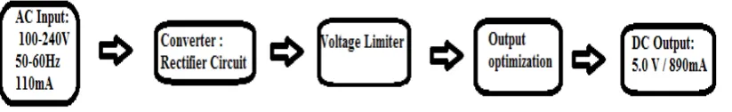
Conventional cell phone chargers available in the market operate at AC input ranging from 100 Volts to 240 Volts and 110 miliampere at 50-60 Hertz producing DC output of 5 Volts and 890 miliampere. Figure 1 illustrates the process of conversion to yield the required output. AC input is rectified; then, voltage limiter is employed to clamp voltage. Finally, rectified output is then feed into filter to minimize ripple from the resultant output.
Figure 1 : Block Diagram of Mobile Phone Charger
5
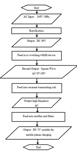
Figure 2 : Block Diagram of Wireless Mobile Phone Charger Start
Rectification
Feed in to switching 43kHz device. AC Input : 240V 50Hz
Output : DC 30V
Desired Output : Square-Wave AC 0V-30V
End
Feed into resonant transmitting coil.
Output high frequency AC
Feed into rectifier and filters
6 Generally, the requirement of load will determine the yield of converters. Thus, a study on the output of required converter is reviewed.
2.2.1. Rectifiers
[3] stated, in general, there are 2 main types of rectifiers, namely the Half-Wave Rectifiers and the Full-Wave Rectifiers.
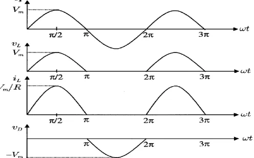
A half-wave rectifier circuit is depicted in Figure 3. Circuit consists of 1 diode fed with transformer secondary voltage. During positive half of power cycle, diode D conducts. Diode D blocks away the negative half of the power cycle.
Figure 3 : Half-Wave Rectifier with resistive load. [3]
Figure 4 depicts the voltage and current waveforms of the half-wave rectifier with resistive loads. It is noticeable the half of a power cycle is lost in the rectification process. Thus, the resultant output will greatly reduce the efficiency of the rectifier.
7
A full-wave bridge rectifier is illustrated in Figure 5. Full-wave bridge rectifier employed four diodes in the rectification process. The positive half cycle of the transformer secondary voltage, diodes D1 and D2 conduct, whereas the negative half cycle, current flows through D3 and D4. Figure 6 illustrates the voltage and current waveforms of full-wave bridge rectifiers.
Figure 5 : Full-Wave Bridge Rectifier with resistive load. [3]
Figure 6 : Voltage and current waveforms of full-wave bridge rectifier. [3]
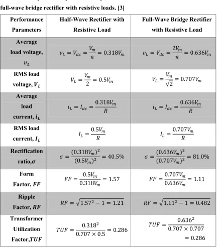
8 Table 1 shows the comparison of performance parameters between half-wave rectifier and full-wave bridge rectifier with resistive loads. Judging from these parameters, full-wave bridge rectifier provides higher power efficiency throughout the rectification process.
Table 1 : Comparison of performance parameters between half-wave rectifier and full-wave bridge rectifier with resistive loads. [3]
Performance Parameters
Half-Wave Rectifier with Resistive Load
Full-Wave Bridge Rectifier with Resistive Load Average load voltage, RMS load
voltage, √
Average load current, RMS load current, Rectification ratio, Form Factor, Ripple
![Figure 5 : Full-Wave Bridge Rectifier with resistive load. [3]](https://thumb-ap.123doks.com/thumbv2/123dok/573379.67925/23.595.166.448.396.643/figure-wave-bridge-rectifier-resistive-load.webp)