FINAL YEAR PROJECT REPORT
DESIGN THE LOW PASS PASSIVE FILTER FOR GRID CONNECTED SINGLE-PHASE VOLTAGE SOURCE INVERTER SYSTEM
STUDENT’S NAME : MUHAMMAD FAID BIN MUSTAFFA
MATRIC NO : B011010246
COURSE : POWER ELECTRONICS AND DRIVES (BEKE)
SUPERVISOR’S NAME : PUAN MAASPALIZA BINTI AZRI
“I hereby declare that I have read through this report entitle “Design The Low Pass Passive Filter for Grid Connected Single-Phase Voltage Source Inverter System” and found that it has comply the partial fulfillment for awarding the degree of Bachelor of Electrical Engineering (Power Electronics and Drives)”
Signature : ………
Supervisor’s Name : Maaspaliza Binti Azri
DESIGN THE LOW PASS PASSIVE FILTER FOR GRID CONNECTED SINGLE-PHASE VOLTAGE SOURCE INVERTER SYSTEM
MUHAMMAD FAID BIN MUSTAFFA
A report submitted in partial fulfillment of the requirement for the degree of Bachelor in Electrical Engineering
(Power Electronics and Drives)
Faculty of Electrical Engineering
UNIVERSITI TEKNIKAL MALAYSIA MELAKA
I declare that this report entitle “Design The Low Pass Passive Filter for Grid Connected Single-Phase Voltage Source Inverter System" is the result of my own research except as cited in the reference. The report has not been accepted for any degree and is not concurrently submitted in candidature of any other degree.
Signature : ………
Name : Muhammad Faid Bin Mustaffa
DEDICATION
This report is dedicated to my parents
ACKNOWLEDGEMENT
I would like to gratitude to Allah S.W.T for His generous blessing and undying strength bestowed upon me during the completion of this project.
I would like to express my special gratitude and thanks towards Puan Maaspaliza Binti Azri as my supervisor for giving me such attention and time. I have taken efforts in this project. However, it would be impossible for me to complete this project without her guidance and constant supervision as well as providing necessary information regarding the project.
ABSTRACT
ABSTRAK
TABLE OF CONTENT
ACKNOWLEDGEMENT ii
ABSTRACT iii
TABLE OF CONTENTS v
LIST OF TABLES ix
LIST OF FIGURES x
CHAPTER 1: INTRODUCTION 1.1 Project Background 1
1.2 Problem Statement 2
1.3 Objectives 3 1.4 Scope 3
1.5 Report Outlines 4
CHAPTER 2: LITERATURE REVIEW 2.1 Introduction 5
2.2 Theory 5 2.2.1 Electrical Grid System 5 2.2.2 Voltage Source Inverter (VSI) 6
2.2.4 Pulse Width Modulation (PWM) & Total Harmonic Distortion (THD) 13
2.2.5 MATLAB Software 13
2.3 Related Previous Works 14
2.4 Summary of Review 14
CHAPTER 3: DESIGN METHODOLOGY 3.1 Introduction 15
3.2 Project Methodology 16
3.3 Simulation Approach 18
3.4 Designing L Filter using Calculation Method 18
3.5 Designing LC Filter using Calculation Method 21
3.6 Designing LCL Filter using Calculation Method 22
3.7 Analysis Based on Switching Frequency 26
3.8 Analysis Based on Modulation Index 27
3.9 Analysis Based on Ripple Current 27
3.10 Analysis Based on Transfer Function and Bode Plot 28
3.11 Summary of Project Methodology 28
CHAPTER 4: RESULT & DISCUSSION 4.1 Introduction 29
4.2 Simulation Result of Circuit Designed Without Filter 30
4.3 Simulation Result of Filter Circuit Designed by using Calculation Method 30
4.3.1 L Filter 31
4.4 Filter Circuit Design Analysis based on Switching Frequency 34
4.4.1 L Filter 34
4.4.1.1 Switching Frequency, fsw 1 kHz 34
4.4.1.2 Switching Frequency, fsw 5 kHz 35
4.4.1.3 Switching Frequency, fsw 10 kHz 35
4.4.1.4 Switching Frequency, fsw 14 kHz 36
4.4.1.5 Switching Frequency, fsw 20 kHz 36
4.4.1.6 Discussion on Switching Frequency Analysis of L Filter 37
4.4.2 LC Filter 39
4.4.2.1 Switching Frequency, fsw 1 kHz 39
4.4.2.2 Switching Frequency, fsw 5 kHz 40
4.4.2.3 Switching Frequency, fsw 10 kHz 40
4.4.2.4 Switching Frequency, fsw 14 kHz 41
4.4.2.5 Switching Frequency, fsw 20 kHz 41
4.4.2.6 Discussion on Switching Frequency Analysis of LC Filter 42
4.4.3 LCL Filter 44
4.4.3.1 Switching Frequency, fsw 1 kHz 44
4.4.3.2 Switching Frequency, fsw 5 kHz 45
4.4.3.3 Switching Frequency, fsw 10 kHz 45
4.4.3.4 Switching Frequency, fsw 14 kHz 46
4.4.3.5 Switching Frequency, fsw 20 kHz 46
4.4.3.6 Discussion on Switching Frequency Analysis of LCL Filter 47
4.5 Filter Circuit Design Analysis based on Modulation Index 49
4.5.1 L Filter 49
4.5.2 LC Filter 51
4.5.3 LCL Filter 52
4.5.4 Discussion on Modulation Index Analysis 53
4.6 Filter Circuit Design Analysis based on Ripple Current 54
4.6.1 L Filter 54
4.6.2 LC Filter 55
4.6.3 LCL Filter 56
4.6.4 Discussion on Ripple Current Analysis 57
4.7 Filter Circuit Design Analysis by using Transfer Function & Bode Plot 57
4.7.1 L Filter 57
4.7.2 LC Filter 60
4.7.3 LCL Filter 63
4.7.4 Discussion based on Transfer Function and Bode Plot 68
CHAPTER 5: CONCLUSION & RECOMMENDATION 5.1 Report Conclusion and Recommendation 69
LIST OF TABLES
2.0 Output Voltage, vobased on Switches Condition 9
3.0 Parameters Values 20
4.0 Percentage of THDi for Different Switching Frequency, fsw for L Filter 37
4.1 Percentage of THDi for Different Switching Frequency, fsw for LC Filter 42
4.2 Percentage of THDi for Different Switching Frequency, fsw for LCL Filter 47
4.3 Percentage of THDi for Different Modulation Index, ma for L Filter 50
4.4 Percentage of THDi for Different Modulation Index, ma for LC Filter 51
4.5 Percentage of THDi for Different Modulation Index, ma for LCL Filter 52
LIST OF FIGURES
2.0 Schematic Diagram of Half-Bridge VSI 7
2.1 Sine-Triangle Comparison 8 2.2 Switching Pulses after Comparison 8 2.3 Schematic Diagram of Full-Bridge VSI 8
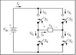
2.4 (a) Equivalent Circuit when Switches S1 and S2 are ON 9
2.4 (b) Equivalent Circuit when Switches S3 and S4 are ON 9
2.4 (c) Equivalent Circuit when Switches S1 and S3 are ON 9
2.4 (d) Equivalent Circuit when Switches S2 and S4 are ON 9
2.5 Circuit Configuration of a Three Element Filter 11
2.6 Circuit with L Filter 11
2.7 Circuit with LC Filter 12
2.8 Circuit with LCL Filter 12
3.0 Block Diagram for Basic Idea of This Project 15
3.1 Flowchart of Project Methodology 16
3.2 Designed Circuit of L Filter 21
3.3 Designed Circuit of LC Filter 22
4.1 Simulation Result for Circuit Design with L Filter 31
4.2 Simulation Result for Circuit Design with LC Filter 32
4.3 Simulation Result for Circuit Design with LCL Filter 33
4.4 Simulation Result for L Filter with 1 kHz 34
4.5 Simulation Result for L Filter with 5 kHz 35
4.6 Simulation Result for L Filter with 10 kHz 35
4.7 Simulation Result for L Filter with 14 kHz 36
4.8 Simulation Result for L Filter with 20 kHz 36
4.9 Graph of Switching Frequency, fsw Vs Total Harmonic Distortion Current (THDi) 38
for L Filter 4.10 Simulation Result for LC Filter with 1 kHz 39
4.11 Simulation Result for LC Filter with 5 kHz 40
4.12 Simulation Result for LC Filter with 10 kHz 40
4.13 Simulation Result for LC Filter with 14 kHz 41
4.14 Simulation Result for LC Filter with 20 kHz 41
4.15 Graph of Switching Frequency, fsw Vs Total Harmonic Distortion Current (THDi) 43
for LC Filter 4.16 Simulation Result for LCL Filter with 1 kHz 44
4.17 Simulation Result for LCL Filter with 5 kHz 45
4.18 Simulation Result for LCL Filter with 10 kHz 45
4.19 Simulation Result for LCL Filter with 14 kHz 46
4.20 Simulation Result for LCL Filter with 20 kHz 46
(THDi) for LCL Filter
4.22 Graph of Modulation Index, ma Vs Total Harmonic Distortion Current 50
(THDi) for L Filter 4.23 Graph of Modulation Index, ma Vs Total Harmonic Distortion Current 51
(THDi) for LC Filter 4.24 Graph of Modulation Index, ma Vs Total Harmonic Distortion Current 53
(THDi) for LCL Filter 4.25 Ripple Current of L Filter 54
4.26 Ripple Current of LC Filter 55
4.27 Ripple Current of LCL Filter 56
4.28 Representative Circuit of L Filter 58
4.29 Transfer Function of L Filter in MATLAB Command Window 59
4.30 Bode Plot of L Filter 59
4.31 Representative Circuit of LC Filter 62
4.32 Transfer Function of LC Filter in MATLAB Command Window 62
4.33 Bode Plot of LC Filter 62
4.34 Representative Circuit of LCL Filter 63
4.35 Transfer Function of LCL Filter in MATLAB Command Window 66
4.36 Bode Plot of LCL Filter 66
4.37 Bode Plot of LCL Filter with R3 = 20 Ω 67
4.38 Bode Plot of LCL Filter with R3 = 1 Ω 67
CHAPTER 1
INTRODUCTION
1.1 Project Background.
An electrical grid is a system that consists of electricity generation, transmission, distribution and control networks. This interconnected network is very important to deliver electricity from suppliers to consumers. In this network system, there are power stations that generate electrical power, transmission lines that transmit power from the power stations to the housing area and industrial area, and distribution lines that supply electrical source to the consumers. The acquisition of the electrical energy from renewable sources is very popular these days and the applications for renewable energy generation undergo rapid development. The using of renewable energy can help reduce the greenhouse gases in atmosphere. These benefits of using renewable energy has make Distribution Resources (DR) rapidly growing in modern distribution network. Many of these resources provide electrical energy in the form of Direct Current (DC) voltage source.
minimizing install time, eliminating interconnected power cabling costs, and reducing building floor space [1].
The filter is very important to be added at the output of VSI in order to limit the current harmonics supplied to the grid system. This makes filtering of non-sinusoidal nature voltage output of VSI is crucial. Basically, filters are used to improve the output waveform of VSI and make it a sinusoidal waveform. A passive ac low pass filter is the most suitable type of filter for this purpose. Basically, to design a good low pass filter, the best filter must produce a total harmonic distortion (THDi) current which satisfies the power quality standard IEEE-519.
Based on standard of IEEE-519, the THD current is limited to 5 % [2].
The method used to design ac low pass filter is very important criteria in order to get the best design by using the easiest technique. There are many method can be used in designing the ac low pass filter such as transfer function method, calculation method and bode plot method. Each method used must fulfil the recommended THDi requirement based on
IEEE-519 standard.
1.2 Problem Statement.
The technology advancements in industrial control processes have increased the demanding requirements on the power quality from the industrial power consumers. Among the arising power quality problems, harmonics is one of the problems that need to be control in electrical power systems. In designing an ac low pass filter, harmonics is one of the important power quality problems which needed to be considered. In designing ac low pass filters, it is difficult to propose a design that can meet the THD current requirement of IEEE-519 (THDi <
The objectives of this project are:
To design the L, LC and LCL low pass filters by using calculation method.
To design low pass passive filters that can satisfy the requirement of THD current based on IEEE-519 which stated that total harmonic current and voltage THDi and
THDv must be less than 5%.
To analyse the performance of L, LC and LCL low pass filter using the MATLAB/Simulink software and also by using transfer function and bode plot in MATLAB M-files.
1.4 Scope.
1.5 Report Outlines. Chapter 1: Introduction.
This chapter presents the background of electrical grid system, voltage source inverter (VSI), passive low pass ac filter, and the various methods to design low pass filter. Moreover, problem statement, objectives, report outlines are been explained in this chapter.
Chapter 2: Literature Review.
In this chapter, theory about electrical grid system, VSI, ac low pass filter, and method of designing low pass filter is been discussed. Related previous works that has been done by others over the past few years also been reviewed and the summary of that review is created.
Chapter 3: Design Methodology.
Project methodology is described in this chapter. The circuits design of ac low pass filter such as L, LC and LCL are presented. The method used to design low pass filter that is the calculation method are analysed. MATLAB software is used for the simulation approach of low pass filter circuits design.
Chapter 4: Result and Discussion.
Chapter 4 shows the output result of from MATLAB simulation and discussions on which type of circuit design ac low pass filter can give THD current that satisfy IEEE-519 standard (THDi < 5%). Besides that, the analyses of L, LC and LCL filter are made by using the circuit
designed in MATLAB and the performances of each filter circuit are examined by using transfer function and bode plot.
Chapter 5: Conclusions.
CHAPTER 2
LITERATURE REVIEW
2.1 Introduction.
This chapter reviews all the theory that related to this project. The systems or components that involve in this project such as electrical grid connected system, VSI, and low pass filer topology are explained in this chapter. Furthermore, the MATLAB software which is used to simulate the circuit design of low pass filter is been exposed in this chapter. In this chapter, the previous works or researches that related to this project are also been presented. Finally, all the important information gathered from theory and previous related works are summarised in ‘Summary of Review’ section.
2.2 Theory.
This section discuss about the components or systems which involve in this project such as electrical grid system, voltage source inverter (VSI), low pass filter, pulse width modulation (PWM), total harmonic distortion (THD), and MATLAB software.
2.2.1 Electrical Grid System.
line, and distribution line. Generating stations are the place where electrical power is produce. Transmission line is the high voltage line that carries power from distant sources to demand centres, while distribution line is the line that distributes electricity to many types of consumers.
Normally, the electricity is generates by fossil fuels which produce ac voltage source. Considering the high consumption of fossil fuels in recent years and this will make this type of source quickly finish. Since fossil fuels consumption increases emission of carbon dioxide, this will results in global warming. Energy crisis and increasing of greenhouse gases have caused the renewable energy resources to be the better power source for modern distribution network [3]. These renewable sources of energy such as water, wind and solar should be used. The dispersed nature of these resources, sometimes called Distribution Resources (DR). Most of DRs produce electrical energy in the form of dc voltage source [3].
2.2.2 Voltage Source Inverter (VSI).
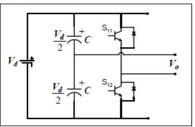
speed ac drives, induction heating, standby aircraft power supplies, uninterruptible power supplies (UPS) for computers and others. The inverter is used to control the fundamental voltage magnitude and the frequency of the AC output voltage. AC loads such as induction motor is required constant or adjustable voltage at their input terminals. This requirement can be fulfilled when such loads are fed by inverter. The schematic diagram for half-bridge circuit for single-phase VSI is shown in Figure 2.0 [4].
Figure 2.0: Schematic Diagram of Half-Bridge VSI.
The pulse width modulation (PWM) scheme is illustrated in Figure 2.1 [4], in which vc is the
peak value of triangular carrier wave and vr is the reference or modulating signal. The
switches S11 and S12 are controlled based on the comparison of sinusoidal signal and the triangular wave which mixed in a comparator. When sinusoidal wave has magnitude higher than the triangular wave the comparator output is high, otherwise it is low. The switching pulse after comparison is shown in Figure 2.2 [4].
v v is on, v (2.0)
and
Figure 2.1: Sine-Triangle Comparison.
Figure 2.2: Switching Pulses after Comparison.