UNIVERS FACULTY O
IMPLEMENTATION OF (SVPWM) FOR THREE
Mu Bachelor of E
VERSITI TEKNIKAL MALAYSIA MELAKA Y OF ELECTRICAL ENGINEERING (FKE)
FINAL YEAR PROJECT TECHNICAL REPORT
N OF SPACE VECTOR PULSE WIDTH MODUL REE PHASE VOLTAGE SOURCE INVERTER US
MATLAB/SIMULINK
Muhammad Asyraf Bin Zulkepple
of Electrical Engineering Industrial Power July 2012
i
)
ii
SUPERVISOR'S DECLARATION
I hereby declare that I have checked this project and in my opinion, this project is adequate in terms of scope and quality for the awards of the Degree of Bachelor of Electrical
Engineering Industrial Power
Signature :
Name : Ir. ROSLI BIN OMAR
Position : Senior Lecturer
iii
IMPLEMENTATION OF SPACE VECTOR PULSE WIDTH MODULATION (SVPWM) FOR THREE PHASE VOLTAGE SOURCE INVERTER USING
MATLAB/SIMULINK
MUHAMMAD ASYRAF BIN ZULKEPPLE
This Technical Report for Final Year Project is submitted to Faculty of Electrical Engineering,
Universiti Teknikal Malaysia Melaka
In partial to fulfilment Bachelor of Electrical Engineering Industrial Power.
Faculty of Electrical Engineering (FKE)
UNIVERSITI TEKNIKAL MALAYSIA MELAKA (UTeM)
iv
STUDENT'S DECLARATION
I hereby declare that this thesis entitled“ImplementationOf Space Vector Pulse Width Modulation (Svpwm) For Three Phase Voltage Source Inverter Using Matlab/Simulink" is the result of my own research except as cited in the references. This is project is adequate
in terms of scope and quality for the award of the degree Bachelor of Electrical Engineering Industrial Power.
Signature :
Name : MUHAMMAD ASYRAF BIN ZULKEPPLE
ID Number : B010910185
v
ACKNOWLEDGEMENT
vi
ABSTRACT
vii
ABSTRAK
viii
1 CHAPTER 1–INTRODUCTION 1.1 Project Background
2 CHAPTER 2–LITERATURE REVIEW 2.1 Pulse Width Modulation
2.2 Sinusoidal Pulse Width Modulation 2.3 Space Vector Pulse Width Modulation
4 7 9
3 CHAPTER 3–METHODOLOGY 3.1 Introduction
4 CHAPTER 4–PROJECT DEVELOPMENT 4.1 Build SIMULINK Model
4.1.1 Time Duration
4.1.2 Calculation Vd, Vq, Vrefand angle 4.1.3 Calculation Time Duration T1, T2, T3
ix
5 CHAPTER 5–SIMULATION RESULT 5.1 Subsystem Making Switching Time 5.2 Subsystem Space Vector PWM Generator 5.3 SIMULINK Model for Overall System
22 24 27 5.4 SIMULINK Model for Sinusoidal Pulse Width Modulation
5.5Analysis Impulse Of Switching
5.6 Analysis Total Harmonics Distortion (THD) 5.7 Analysis Data Total Harmonics Distortion (THD)
30 32 33 34
6 CHAPTER 6–CONCLUSION
x
LIST OF TABLE/ CHART
TABLE/CHART TITLE PAGES
3.3.1 Research Methodology Flow Chart 16
xi
LIST OF FIGURE
FIGURE TITLE PAGES
2.1.1 PWM Inverter 5
2.1.2 PWM Signal Produce and influence command signal to the wider of pulse
5
2.1.3 Pulse Width Modulation 6
2.2 Principle of three phases SPWM 8
2.3.1 Three phase voltage source PWM inverter 9
2.3.2 Eight switching state of inverter voltage vector 10
2.3.3 Representation of topology 1 on plane α -β 11
2.3.4 Non-zero voltage vector onplane α -β 11
2.3.5 Zero voltage vectors on plane α -β 12
2.3.6 output voltage vector on plane α -β and time domain 12
3.2.1 MATLAB logo 14
4.1.1 The relationship between abc frame and dq frame. 19 4.1.3 reference vector as a combination of adjacent vector at sector 1 20
5.1 Making Switching 22
5.1.1 Making Switching at Ta 23
5.1.2 Making Switching at Tb 23
5.1.3 Making Switching at Tc 24
5.2 Space Vector Pulse Width Modulation Generator 24
5.2.1 Inverter output line-to line voltage,VLAB 25
5.2.2 Inverter output line-to line voltage,VLBC 25
5.2.3 Inverter output line-to line voltage,VLCA 26
5.3 5.3.1
SIMULINK Model for overall system Load voltage Line-to-Line
26 27
xii
5.3.3 Inverter output Line-to-Line current 28
5.3.4 Inverter output Phase current. 28
5.3.5
Circuit model of three phase Sinusoidal Pulse Width Modulation Voltage Output at Phase A
Voltage Output at Phase B Voltage Output at Phase C
29
5.6 Effect impulse of switching between SPWM and SVPWM 32
5.7 SPWM THD data 33
xiii
LIST OF APPENDIX
LIST TITLE PAGES
A The Switching Time of Each Transistor 37
B Summarized Switching Time Calculation at Each
Factor. 39
C Gantt chart Final Year Project (FYP) Progress 40
1
CHAPTER 1
INTRODUCTION
Section below focuses on what is expected to be done during the project period. It will also outline the general background, activities done and project goals. Furthermore, in order to give a more deeply concern, it will list out the key reasons for launch and what is the primary concerns that cause this project compulsory to be launched.
1.1 Project Background
Nowadays, the demands for the electronic products are getting higher due to the rapid advances in technology. The usage of electronic appliances now is a part of our lives, where it covers 80% of the performance in our daily activities. For example, we require a computer to find the latest information on recent developments, mobile phones are used to communicate, machines and motors AC / DC are used by both small and large-scale industries to lift or move objects. Most of the electronic equipment is called distortion current also known as non-linear load. This non-linear load might be a single phase or three phase load. For example for the variable speed drives, the current production is called Harmonic distortion [14].
2
1.2 Problem Statement
As stated above, the largest problem in power quality is harmonic distortion. Harmonic distortion is divided into two of the harmonic which are voltage and current harmonics. Harmonic currents produced by the harmonics contained in the supply voltage depending on the types of loads such as resistive load, capacitive load and inductive load. These harmonics can be generated from the source side or load side. Harmonic at the load side is due to the nonlinear operation of electronic devices they include. This can cause magnetic core transformer and motor overheat thus, reduce the efficiency and lifetime of the equipment.
Induction motor drives are widely used in high performance drive system. It is due to the good power factor, high efficiency, extremely rugged and do not require starting motor. This function is to allow the adjustment of speed motor by using the frequency and amplitude of the stator voltage. However, the ratio of stator voltage to frequency should be kept constant [3].
3
1.3 Project Objective
There are several objectives to be accomplished in this project including:
i. To study and do analysis about the concept of inverter, sinusoidal pulse width modulation (SPWM) and space vector pulse width modulation (SVPWM).
ii. To study and investigate model of a three phase voltage source inverter (VSI) based on space vector concept.
iii. To design the suitable model SVPWM.
iv. To develop step by step and do simulation model of SVPWM.
1.4 Project Scope
There are several types modulating technique that controls the amount of time and the sequence that uses to switch on and off. The most modulating techniques used are the carrier-based technique. For example the sinusoidal pulse width modulation (SPWM), the space-vector (SV) technique, and the selective-harmonic-elimination (SHE) technique. The scope of this project is focused on the implementation of SVPWM for three phase voltage source inverter using the software MATLAB/SIMULINK this includes:
i. Focus on development of MATLAB/SIMULINK model of SVPWM step by step. ii. Investigated model of a three phase voltage source inverter (VSI) based on space
vector.
4
CHAPTER 2
LITERATURE REVIEW
This chapter will discuss about the review done on several related article which includes the previous project and the method that use to solve the problem. The review will contain the theory that had been carried out by each article. The review is conducted among three (3) major articles which are:
i. Project space vector PWM inverter [2].
ii. Control of voltage source inverter using PWM/SVPWM for adjustable speed drive applications [1].
iii. MATLAB/SIMULINK model of space vector PWM for three phase voltage source inverter [12].
2.1 Pulse Width Modulation
PWM modulation is a technique developed by a combination of electronic components circuit to generate a variable analogue signal. It uses a simple concept where they open and close the switch at different intervals.
Based on the Figure 2.1. while switch S3 and S4 are O now are ON and switch S1 and S
Figure 2.1.2: PWM S
Figure 2.1.1: PWM Inverter [8].
2.1.1 above, on the positive cycle switch S1 and S OFF. Different on the negative cycle where swit 1 and S2 will OFF. It will produce a full wave output
Signal Produce and influence command signal of pulse [9].
5
nd S2 will be ON witch S3 and S4
put.
6
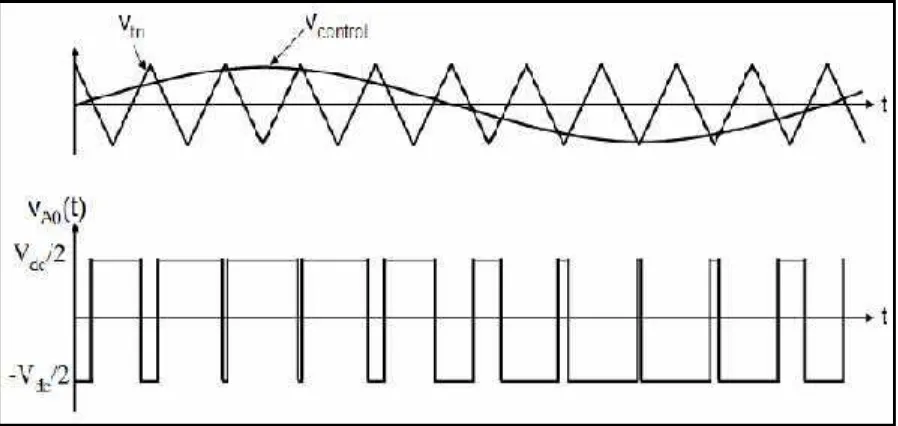
The output of PWM signal is produce from the comparison between two different signal which are modulating signal (sinusoidal wave) and carrier signal (saw tooth wave). This comparison process is done by the comparator. The frequency size of PWM output signal is varying based on the size of intersection between carriers and modulating signal as Figure 2.1.2. Below will show the derivation of inverter output voltage:
Figure 2.1.3: Pulse Width Modulation [8].
When > , = /2
When < , = − /2
Modulation index (m) defined as:
=VcontrolVtri =
7
The major advantages of Pulse Width Modulation Inverter:
i. Will make efficiency up to 90%. PWM will developed higher torque inside the motor in which use to overcome the internal motor resistance in simplest way. ii. Lower order harmonics can be eliminate or minimized along with its output voltage.
Efficient when used to convert voltages or to dim light bulbs.
iii. Low power consumption. PWM will reduce the harmonic distortion means that stabilize the frequency and current, so it will save the power.
The disadvantages of Pulse Width Modulation Inverter:
i. Increase of switching losses due to high PWM frequency.
ii. Electromagnetic interface problems due to high order harmonics.
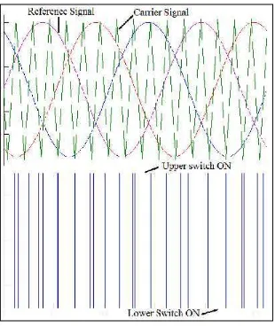
2.2 Sinusoidal Pulse Width Modulation
8
Figure 2.2: Principle of three phases SPWM.
The frequency of reference signal is used to determine the inverter output frequency, and it peak amplitude control the modulation index, M1 and then in turn the output voltage. By varying the modulation indexM1, the output voltage can be varied [8].
, 1 = ℎ ℎ
= ( − 1)
Where:
9
Output voltage, Vout= M1Vin
Modulation ratio, Mr
=
2.3 Space Vector Pulse Width Modulation
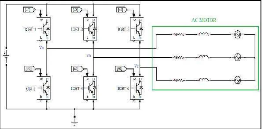
Space Vector PWM refers to a special switching sequence of the upper three power transistor of a three phase power inverter. It used to generate less harmonic distortion in the output voltages and current applied to the phases of an AC motor and to provide more efficient use of supply voltage compared with sinusoidal modulation technique [2]. The SVPWM circuit can be modelling by three phase voltage source PWM inverter as shown Figure 2.3.1.
Figure 2.3.1: Three phase voltage source PWM inverter
10
topologies. This topology is happen because of the switch controller at IGBT gate, which is switch, is ON and OFF condition during the certain time interval. Figure 2.3.2 show switching state of inverter.
Figure 2.3.2: Eight switching state of inverter voltage vector. [2]
Zero switching state occurs at V0and V7, which the upper three switches (S1, S3, S5) are operate together or the three switch lower side (S2, S4, and S6) are operate at the same time. For non-zero switching state the upper side switch and lower side switch must move by alternate operate or interval to obtain the continuous output circuit (only one switch may be closed per phase leg in order to prevent a short circuit) [2].
From Figure 2.3.2 space vector modulation can be represent at plane α -β . For
example from topology V1the line voltages and are given: Vab= Vg
11
Figure 2.3.3: Representation of topology 1 on plane α -β [2].
From figure 2.3.3thevalue of three line voltage vector plotted on plane α -β and the
vector produce represented as, V1. Proceeding on the similar plane the six non-zero voltages vector can be shown to assume the position of vector in regular hexagon (dotted line) as Figure 2.3.4 [1].
Figure 2.3.4: Non-zero voltage vector on plane α -β [2].
For zero voltage vectors, the vector represented as zero magnitude, it refer to the zero switching state. For example:
![Figure 2.1.1: PWM Inverter [8].](https://thumb-ap.123doks.com/thumbv2/123dok/567290.67058/18.612.132.481.383.671/figure-pwm-inverter.webp)
![Figure 2.3.2: Eight switching state of inverter voltage vector. [2]](https://thumb-ap.123doks.com/thumbv2/123dok/567290.67058/23.612.152.493.137.445/figure-switching-state-inverter-voltage-vector.webp)
![Figure 2.3.3: Representation of topology 1 on plane α-β [2].](https://thumb-ap.123doks.com/thumbv2/123dok/567290.67058/24.612.184.468.363.576/figure-representation-of-topology-on-plane-a-b.webp)
