MATLAB/SIMULINK BASED ANALYSIS OF
VOLTAGE SOURCE INVERTER WITH SPACE VECTOR
MODULATION
Auzani Jidin1, Tole Sutikno2
1
Department of Power Electronics and Drives, Faculty of Electrical Engineering Universiti Teknikal Melaka Malaysia (UTeM), 75450 Ayer Keroh, Melaka, Malaysia
2
Department of Electrical Engineering, Faculty of Industrial Technology Universitas Ahmad Dahlan (UAD), Yogyakarta 55164, Indonesia
e-mail: [email protected]1, [email protected]2
Abstrak
Modulasi vector ruang (space vector modulation, SVM) adalah teknik modulasi terbaik untuk kemudi beban tiga fasa seperti motor induksi 3 fasa. Pada paper ini, strategi modulasi lebar pulsa dengan SVM dianalisis secara detail. Strategi modulasi ini menggunakan kalkulasi waktu switching untuk menghitung waktu tegangan vektor yang diterapkan pada beban tiga fasa seimbang. Prinsip strategi modulasi vektor ruang ini disimulasikan dengan perangkat lunak Matlab/Simulink. Hasil simulasi menunjukkan bahwa algoritma ini adalah fleksibel dan cocok digunakan untuk kendali vector lanjut. Strategi switching ini meminimalkan distorsi beban sebaik meminimalkan kerugian akibat jumlah komutasi pada inverter.
Kata kunci: distorsi harmonik, inverter, komutasi vetor, modulasi vector ruang
Abstract
Space vector modulation (SVM) is the best modulation technique to drive 3-phase load such as 3-phase induction motor. In this paper, the pulse width modulation strategy with SVM is analyzed in detail. The modulation strategy uses switching time calculator to calculate the timing of voltage vector applied to the three-phase balanced-load. The principle of the space vector modulation strategy is performed using Matlab/Simulink. The simulation result indicates that this algorithm is flexible and suitable to use for advance vector control. The strategy of the switching minimizes the distortion of load current as well as loss due to minimize number of commutations in the inverter.
Keywords: harmonics distortion, inverter, space vector modulation, vector commutations.
1. INTRODUCTION
Due to the growing of fast processor, many researches today show great interest to develop new or to modify PWM control algorithm to obtain good performances of ac drives. The conventional PWM method known as sinusoidal pulse-width modulation (SPWM) is one of the simple technique in voltage source inverter (VSI). This technique applies simple control strategy by comparing the three-phase modulated signals (known as reference signal) with carrier signal. In this technique the switching frequency is depends on the carrier switching. The amplitude output voltage can be varied by controlling the modulation index defines as in [1].
step six , 1
1 −
=
V
V
M
i(1) Traditionally the SPWM technique is widely used in variable speed drive of induction
even with simple analogue ICs circuits. However, this algorithm has the following drawbacks. This technique is unable to fully utilize the available DC bus supply voltage to the VSI. This technique gives more total harmonic distortion (THD), this algorithm does not smooth the progress of future development of vector control implementation of ac drive. These drawbacks lead to development of a sophisticated PWM algorithm which is Space Vector Modulation (SVM). This algorithm gives 15% more voltage output compare to the sinusoidal PWM algorithm, thereby increasing the DC bus utilization. Furthermore, it minimizes the THD as well as loss due to minimize number of commutations in the inverter. This algorithm has been modified to improve the ac drive performances by many researchers as in [2-6] and [7]. For instance, the SVM has wide prospect of research that need to explore especially to improve dynamic performance in overmodulation range and for matrix converter applications.
2. SPACE VECTOR MODULATION
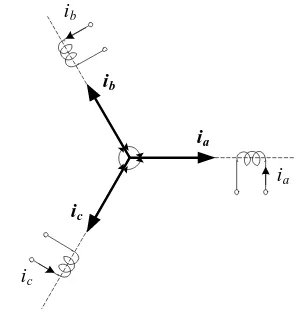
The three-phase line to neutral sine waves required for 3-phase load can be represented as 1200 phase-shifted vectors (va, vb and vc) in space as shown in Figure 1. For a balanced load, 3-phase connected system, these vectors sum to zero. At any time instant the three-phase load voltages can be expressed by a single space reference vector v* as shown in figure 1. In space vector modulation strategy, the motor frequency and the motor voltage can be controlled by controlling the amplitude and the frequency of v*. This PWM control strategy of the inverter can be applied to the various technique of ac motor drive such as scalar control, field oriented control and direct torque control.
Figure 1. Three-phase voltage vectors and the resultant space reference vector
Figure 2 The vector of three-phase stator currents
In this section the manipulation of space vector is discussed. To understand easily the manipulation of space vector, the three-phase stator current of the induction motor are used as shown in Figure 2. The induction motor is considered Y connection and ia, ib and ic are the phase stator current. Each coil of the stator produces a sinusoidally distributed mmf. These phase stator currents vector can be added vectorially and gives equation 2.
(
a b c)
s
i
i
i
i
=
+
+
3
2
(2) where is is an instantaneous quantity and it is not a phasor quantity. The is can be written as a
complex number,
=
s
i
i
se
jθ(3) ia
ib
ic
ia ib
ic va
vb
vc
1200
and in steady state, the is is expressed as
=
s
i
i
se
j tω
(4) By using Euler theorem the three-phase stator phase currents are expressed as
a
i
aj a
e
i
i
=
=
00b
i
j bb
e
ai
i
=
=
1200c
i
j cc
e
a
i
i
2400=
2=
(5)By substituting equation (4) into equation (1), the following equation is obtained
s
i
(
i
aai
ba
i
c)
2
3
2
+
+
=
(6) To determine the resultant vector or space reference vector of the three-phase voltages
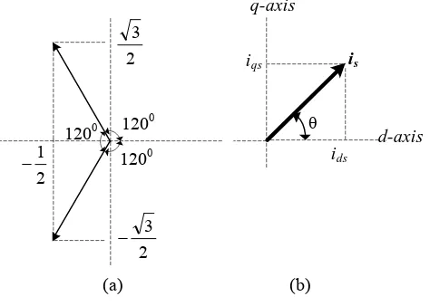
and currents, it is important to transform the three-phase vectors to d-q axis. This process is popularly known as Park Transformation. The rectangular coordinate in Figure 3 (a) shows how the complex vectors can be transformed into real and imaginary components.
Figure 3. The complex vector, (a) in rectangular coordinates, (b) space reference vector
From equation (4), by applying the Euler Theorem, the real and imaginary components can be obtained as
2
3
2
1
0 120
j
e
a
=
j=
−
+
and
2
3
2
1
0 240 2
j
e
a
=
=
−
−
(7) Separate into real and imaginary terms and hence the expressions for the two axis currents in
terms of the three-phase currents can be determined as
(a) (b)
ids
d-axis q-axis
θ
iqs is
2 3
2 3
−
2 1
−
1200
s
i ia ib ic⎟⎠+ j
(
ib−ic)
=ids+ jiqs ⎞ ⎜ ⎝ ⎛ − − = 3 1 3 1 3 1 3 2 (8)Therefore, the space reference vector can be obtained using Pythagoras Theorem as depicted in Figure 3(b).
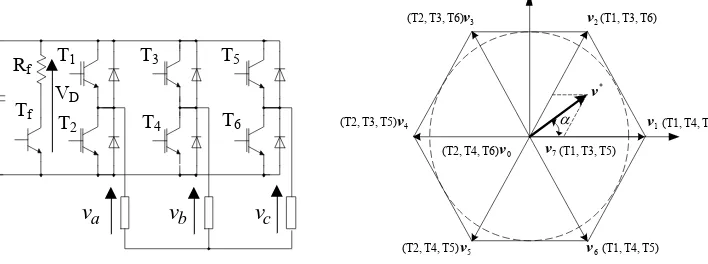
The power circuit of the inverter consists of six-IGBT T1, T2, T3, T4, T5, T6 with their
anti parallel diodes as shown in Figure 4. The circuit also included the braking resistance Rf and the braking transistor Tf. These elements dissipate the energy regenerated by the inverter. The load is considered as Y-connected in order to make clear understanding about principle of modulation technique.
Figure 4. Power Circuit of the Inverter
Figure 5. Space Vector hexagon
Similarly, the voltage vector of the load voltages (va, vb and vc), for the three-phase balanced load is
(
va avb a vc)
2 3 2 + + = v (9) with 0 240 0 120 , j j e a e
a= =
The inverter bridge shown in Figure 4, uses six IGBTs switches. For safe operation of the VSI, whenever one switch of a half bridge is turn on, the other switch of the same half bridge must be off and vice versa. That is mean three independent PWMs are generated for the three half bridge. This gives rises to eight distinct switching states of VSI, where states 1 through 6 are called the active states and states 0 and 7 are called the inactive states. The inverter does not generate purely sinusoidal voltages to the load, but depending on switching states of the transistors it generates voltage vectors v0, v1,….,v7 which are shown in space vector hexagon in Figure 5. As seen in Figure 5, the zero voltage vectors have zero voltage amplitude and located at the origin of the hexagon. The space vector hexagon has six sectors which are divided into six equal sized sectors of 600. Each sector is bounded by two active vectors. The locus of the circle is projected by the space vector v* depends on v0, v1,….,v7 . Mathematically, it can be represented by equation 10.
* v =
∑
=⎜⎜⎝
⎛
⎟⎟⎠
⎞
= 7 7 ... 2 , 1 n n s nT
t
(10) where Ts is the sampling time.1
v (T1,T4,T6) T6) T3, (T1, T6) T3, (T2, T5) T3, (T2, T5) T4,
(T2, (T1,T4,T5) T5) T3, (T1, T6) T4, (T2, 2 v 3 v 4 v 5
v v6
7 v 0 v * v α
x vn
240V
T1 T3
T4 T5 T6 Rf Tf Cf VD a
v vb vc
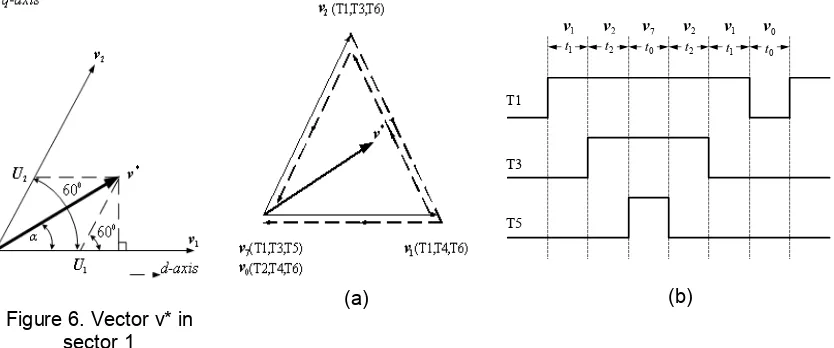
The reference space vector rotates and moves through the different sectors of the complex plane as shown in figure 5 as time t increases. In each PWM cycle, modulation vector v* is sampled at the fixed input sampling frequency 2fs. During this time, the sector is determined and the modulation vector v* is mapped onto two adjacent vectors. Figure 6 shows the reference vector v* in sector 1, with the adjacent vectors v1 and v2. In general the two adjacent vectors in all sectors can be expressed as
vk and vk+1 (11)
where k is which sector that the modulation vector v* lies.
In the vector modulation it is considered that the reference vector v* is constant and stationary in the complex plane, during the sampling interval Ts. As depicted in equation 9, the reference voltage vectors v* is equal to the time average of the voltage vectors applied to the load during the sampling interval Ts (Ts=2fs, where fs is the switching frequency). For example, consider the v* is stationary in sector 1 at a vector angle α as illustrated in figure 6. Using equation 9, the v* can be determined as
0 0 2 1 *
v
T
T
v
T
T
v
T
T
v
s s b sa
+
+
=
(12) where t1, t2 and t0 are the respective on-times to generate voltage vectors v1, v2 and vo.
The times above must fulfill the following equation:
s
c T
t t
t1+ 2+ = (13)
Considering that v0=0, equation (12) gives,
2 1 * v T T v T T v s b s a + = (14)
The equation (13) is verified as seen in figure 6 that
2 1 *
U U
v = + (15)
From figure 6, the amplitude of voltage vectors Ua and Ub is obtained by applying the trigonometric relations α α sin 3 1 cos * *
1 v v
U = −
(16) α sin 3 2 * 2 v U = (17) These component vectors U1 and U2 are used to calculate the amount of time that v1 and v2
vectors are applied during PWM cycle. Considering that
D V v v 3 2 2 1 = =
(18)
using equations (12) to (17), the on-times t1, t2 and to are obtained
s D
a T
V v t
⎟⎟⎠ ⎞ ⎜⎜⎝
⎛ −
= α sinα
3 1 cos 2
3 *
(19)
(
)
s Db T
V v t 3 sinα
*
=
(20)
2 1 0 T t t
t = s− − (21)
It can be clearly seen from equations (18) to (20), that the on-times t1, t2 and to depend on the magnitude and angle of the reference vector v* and on the sampling time Ts.
In [1], the optimization of the switching sequences is proposed by locating the zero voltage vector v7 as the last vector in the switching sequence within a sampling interval and by locating vo as the last vector in the reversion of switching sequence with respect to the sequence of the previous sampling interval. The optimal vector commutation and switching sequences is illustrated in Figure 7.
(a) (b)
Figure 6. Vector v* in sector 1
Figure 7. Optimal vector (a) Optimal vector commutation. (b) Optimal switching sequences.
From figure 7, it can be seen that the change from one vector to another is obtained by switching the transistor in one phase. In this way, the number of commutations and the switching losses in the power semiconductors can be minimized.
3. THE SPACE VECTOR MODULATOR
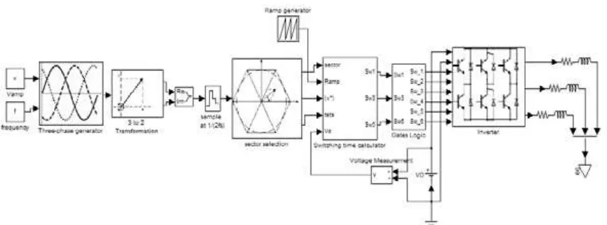
In this section, the description of the space vector modulator is discussed. The space vector modulator is constructed using Matlab/Simulink. The space vector modulator (SVM) contains six blocks, shown in the following figure. These blocks are described below.
The three-phase generator is used to produce three sine waves with variable frequency and amplitude. The three signals are out of phase with each other by 120 degrees. The inverter demanded frequency and voltage are two of the block inputs. The dc voltage to the inverter is measured from the DC bus voltage measurement. This measure is used to compute the voltage vector applied to the motor. The three to two transformations converts voltages from the three-phase to the two-three-phase system using Park’s Transformation Theorem.
The block of vector selection is used to find the sector of the two-axis plane in which the voltage vector lies. The two-axis plane is divided into six different sectors spaced by 60 degrees.
1
v v2 v7 v2 v1 v0 1
t t2 t0 t2 t1 t0
T1
T3
T5
=
1
t
=
2Figure 8. Block diagram of space vector modulator
The ramp generator is used to produce a unitary ramp at the PWM switching frequency. This ramp is used as a time base for the switching sequence. The switching time calculator is used to calculate the timing of the voltage vector applied to the motor (the three-phase resistive-inductive load is represented as three-phase induction motor). The block input is the sector in which the voltage vector lies. The logic gates receive the timing sequence from the switching time calculator and the ramp from the ramp generator. This block compares the ramp and the gate timing signals to activate the inverter switches at the proper time.
4. SIMULATION RESULTS
Simulation results were performed using Simulink block as shown in Figure 8. The dc bus VD is equal to 220V, is connected to the input of the inverter. For the linear operating range the v* must not exceeds the boundary of the hexagon. Therefore the maximum amplitude of the desired v* is calculated as
2 2
max *
6
2
3
2
⎟
⎠
⎞
⎜
⎝
⎛
−
⎟
⎠
⎞
⎜
⎝
⎛
=
V
DV
Dv
(22)
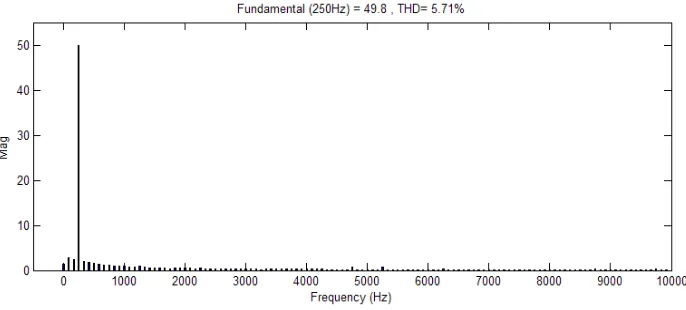
distortion due to switching frequency of 5 kHz. In addition, Figure 11 shows the spectrum of phase current harmonics and gives the THD 5.71%.
Figure 11 Spectrum of phase current harmonics
5. CONCLUSION
Space Vector Modulation only requires one reference space vector to generate three-phase sine waves. The amplitude and frequency of load voltage can be varied by controlling the reference space vector. This algorithm is popularly used in ac drive applications. Furthermore, this algorithm is flexible and suitable to use for advance vector control. The strategy of the switching minimizes the distortion of load current as well as loss due to minimize number of commutations in the inverter.
REFERENCES
[1]. J. Holtz, “Pulse Width Modulation - A Survey”, IEEE Transactions on Industrial Electronics, vol. 38, no. 5, pp. 410-420, 1992.
[2]. A.M. Hava, R.J. Kerkman, and T.A. Lipo, “Simple Analytical and Graphical Tools for Carrier Based PWM Methods”, in IEEE-PESC Conf. Records, St. Louis, Missouri, pp. 1462-1471, 1997.
[3]. S. Ogawawar, H. Akagi, and A. Nabae, “A Novel PWM Scheme of Voltage Source Inverter Based on Space Vector Theory”, in European Power Electronics Conf., Aacheen, Germany, pp. 1197-1202, 1989.
[4]. J. Holtz, W. Lotzkat, and A.M. Khambadkone, “On Continuous Control of PWM Inverters in Overmodulation Range Including The Six-Step”, IEEE Transaction on Power Electronics, vol.8, no.4, pp.546-553, 1993.
[5]. T.G. Habetler, F. Profumo, M. Pastorelli, and M. Tolbert, “Direct Torque Control of Induction Machines Using Space Vector Modulation”, IEEE Trans. On Industry Applications, vol.28, no.5, pp.1045-1053, Sept/Oct, 1992.
[6]. A.M. Khambadkone and J. Holtz, “Current Control in Overmodulation Range for Space Vector Modulation Based Vector Controlled Induction Motor Drives”, in IEEE International Conference on Industrial Electronics, Control, Instrumentation and Automation (IECON 2000), pp.1334-1339, Oct 2000.