MODELING AND SIMULATION OF SPACE VECTOR PULSE WIDTH
MODULATION FOR THREE PHASE VOLTAGE SOURCE INVERTER
NUR SHUHADA BINTI GHAZALI
Bachelor of Electrical Engineering
(Power Electronic And Drives)
" I hereby declare that I have read through this report entitle "Modeling and Simulation of Space Vector Pulse Width Modulation for Three Phase Voltage Source Inverter" and found that it has comply the partial fulfillment for awarding the degree of Bachelor of Electrical Engineering (Power Electronic and Drive) "
Signature : ……….
Supervisor's Name : Dr.Auzani Bin Jidin
MODELING AND SIMULATION OF SPACE VECTOR PULSE WIDTH
MODULATION FOR THREE PHASE VOLTAGE SOURCE INVERTER
NUR SHUHADA BINTI GHAZALI
A report submitted in partial fulfillment of the requirement for the degree
of Bachelor in Electrical Engineering
(Power Electronic and Drive)
Faculty of Electrical Engineering
UNIVERSITI TEKNIKAL MALAYSIA MELAKA
I declare that this report entitle "Modeling and Simulation of Space Vector Pulse Width Modulation for Three Phase Voltage Source Inverter " is the result of my own research except as cited I the reference. The report has not been accepted for any degree and is not concurrently submitted in candidature of any other degree.
Signature : ………
Name : Miss Nur Shuhada Binti Ghazali
ACKNOWLEDGEMENT
ii ABSTRACT
ABSTRAK
iv TABLE OF CONTENTS
CHAPTER TITLE PAGE
ACKNOWLEDGEMENT i
ABSTRACT ii
ABSTRAK iii
LIST OF TABLES vii
LIST OF FIGURES viii
LIST OF ABBREVIATIONS x
LIST OF APPENDICES xi
1 INTRODUCTION 1
1.1 Research Overview 1
1.2 Research Motivation 2
1.3 Problem Statement 2
1.4 Objective 3
1.5. Scope of Research 3
1.6 Report Outline 4
2 LITERITURE REVIEW 5
2.1 Introduction 5
2.2 Voltage Source Inverter 5
2.2.1 Three-Phase Voltage Source Inverter 7
2.3 Pulse Width Modulation 12
3 METHODOLODY 21
3.1 Introduction 21
3.2 Research Methodology 20 3.3 Analytical Approach 25
3.3.1 Implementation Procedure of SVPWM and DSVPWM 25
3.4 Simulation Approach 33
3.4.1 MATLAB/Simulink Model for SVPWM and DSVPWM 33
4 RESULT AND DISCUSSION 43 4.1 Introduction 43
4.2 Simulation Resluts 43
4.2.1 Voltage Vector Plane 43
4.2.2 Switching Pattern 44
4.2.3 Phase Voltage and Phase Current 46
4.2.4 Total Harmonic Distortion 47
4.2.5 Comparison of Efficiency and THD for SVPWM and DSVPWM 50
4.2.7 Switching Frequency 52
5 CONCLUSION AND RECOMMENDATIONS 54
5.1 Conclusion 54 REFERENCES 56
LIST OF TABLE
TABLE TITLE PAGE
Table 2.1 Leg voltage of three-phase VSI during six step mode operation 9
Table 3.1 SVPWM Mapping Vector 32
Table 3.2 DSVPWM Mapping Vector 33
Table 4.1 Comparison of Efficiency and THD for SVPWM and DSVPWM 50
viii LIST OF FIGURE
Figure TITLE PAGE
Figure 2.1 Block diagram of adjustable frequency drive (AFD) 6 Figure 2.2 Power circuit topology of a three-phase voltage source inverter 7 Figure 2.3 Driving switching signal of a three-phase VSI in
six-step mode operation 8
Figure 2.4 Phase-to-Neutral Load Voltage of three-phase VSI 10
Figure 2.5 Phase voltage of three-phase VSI 11
Figure 2.6 Line-to-line Voltage of three-phase VSI 12 Figure 2.7 Three-phase voltage vectors and resultant space voltage vector [5] 13 Figure 2.8 The vector of three-phase stator current [5] 14 Figure 2.9 the complex vector, (a) in rectangular coordinate 15
(b) space reference vector.
Figure 2.10 Space Vector Hexagon 17
Figure 2.11 Voltage V* at sector 1 18
Figure 2.12 the optimization of switching sequence 20
Figure 3.1 Flow chart of overall process 24
Figure 3.2(a) Flow diagram for Space Vector Modulator Implementation 25
Figure 3.2(b) Flow diagram for Space Vector Modulator Implementation 26
Figure 3.3(a) Sector Identification 28
Figure 3.3(b) Alpha Beta Voltage Vector 28
Figure 3.9(a) Flow Chart of Sector Identification and Alpha Beta Voltage Vectors 37 Figure 3.9(b) Flow Chart of Sector Identification and Alpha Beta Voltage Vectors 38 Figure 3.9(c) Flow Chart of Sector Identification and Alpha Beta Voltage Vectors 39 Figure 3.10(a) Duty Ratios Calculation is detail of Subsystem3 for SVPWM 40 Figure 3.10(a) Duty Ratios Calculation is detail of Subsystem3 forD SVPWM 40 Figure 3.11(a) PWM Generation is detail of Subsystem4 for SVPWM 41 Figure 3.11(b) PWM Generation is detail of Subsystem4 for DSVPWM 41 Figure 3.12 Simulation model of comparison performance between SVPWM and 42
DSVPWM based-2-level VSI
Figure 4.1 Voltage Vector Plane 44
Figure 4.2(a) Switching Pattern for Sector 1 of SVPWM 45 Figure 4.2(b) Switching Pattern for Sector 1 of DSVPWM 45
Figure 4.3 Phase voltage for SVPWM and DSVPWM 46
Figure 4.4 Phase current for SVPWM and DSVPWM 47
Figure 4.5 Spectrum of Phase Voltage Harmonic for SVPWM at MI=1 48 Figure 4.6 Spectrum of Phase Voltage Harmonic for DSVPWM at MI=1 48 Figure 4.7 Spectrum of Phase Current Harmonic for SVPWM at MI=1 48 Figure 4.8 Spectrum of Phase Current Harmonic for DSVPWM at MI=1 49 Figure 4.9 Graph of Efficiency Versus Modulation Index for
SVPWM and DSVPWM 51
Figure 4.10 Graph of THD of Voltage versus Modulation Index for
SVPWM and DSVPWM 51
Figure 4.11 Graph of THD of Current versus Modulation Index for
SVPWM and DSVPWM 52
x LIST OF ABBREVIATIONS
MI Modulation Index
SVPWM Space Vector Pulse Width Modulation
DSVPWM Discontinuous Space Vector Pulse Width Modulation VSI Voltage Source Inverter
CSI Current Source Inverter
DC Direct Current
LIST OF APPENDICES
CHAPTER 1
INTRODUCTION
1.1 Research Overview
In the age of globalization era, the great demand in high efficiency industrial applications lead to development of high performance drives technology. The demand urged the researchers to undertake research extensively. The researches discover a technique to improve efficiency of voltage source inverter. Conventionally, space vector pulse width modulation (SVPWM) is the best technique used to control voltage source inverter. A new technique known as discontinuous pulse width modulation (DSVPWM) propose to improve SVPWM technique. The propose technique also famous as two-phase SVPWM. The analysis of these two techniques is focus on efficiency improvement and total harmonic distortion.
1.3 Problem Statement
1.4Objectives
i. To simulate and explain space vector pulse width modulation (SVPWM) and discontinuous space vector pulse width modulation (DSVPWM) technique for three phase voltage source inverter by using MATLAB/SIMULINK.
ii. To analyses the improvement in efficiency of discontinuous space vector pulse width modulation (DSVPWM) over space vector pulse width modulation (SVPWM).
iii. To analyses the Total Harmonic Distortion (THD) for both space vector pulse width modulation (SVPWM) and discontinuous space vector pulse width modulation.
1.4 Scope of Research
There are two approaches in implementation of DSVPWM which is zero voltage (000) eliminated and zero voltage (111) eliminated. Only zero voltage (000) eliminated approach enclosed in this research project. This research project also analyses Total Harmonic Distortion for both SVPWM and DSVPWM technique. This research project focus on the implementation of SVPWM and DSVPWM technique for three-phase voltage source inverter using the software MATLAB/SIMULINK includes:
i. Focus on development of MATLAB/SIMULINK model of SVPWM and DSVPWM step by step.
Chapter 1 Introduction
In this chapter, the brief idea about the project is discuss in overview. The idea is then elaborated in research motivation, objectives, scope as well as contribution of research.
Chapter 2 Literature Review
The review of basic principle PWM technique and the topologies of voltage source inverter are explained in detail. Besides, this chapter summed up the research information in related previous work and summary of review. The software used for simulation is described.
Chapter 3 Methodology
The overall flow of the project is explain and illustrated in flow chart. In addition, the detail of involved step is provided in analogical approach.
Chapter 4 Results and Analysis
The results, analysis and discussion of three-phase VSI using SPWM will be discuss in this chapter.
Chapter 5 Conclusion
CHAPTER 2
LITERATURE REVIEW
2.1 Introduction
This chapter will justify and discusses the source or articles that are associated with the project. It consists of the theoretical information about the technique used. The derivation of Space Vector Pulse Width Modulation (SVPWM) is additionally express in this chapter.
2.2 Voltage source inverter (VSI)
impedance at the DC source.
Voltage source inverter made up of power transistors and their controlled turn ON and turn OFF is generated from self-commutation with base signals. Each power switch of the inverter is insulated gate bipolar transistor (IGBT) with anti-parallel diodes. There are other possible choices of transistor to replace IGBT such as insulated gate commutated thyristors (IGCTs) and injection enhanced gate transistors (IEGTs) but IGBT is widely used in VSI drives market. The IGBT switches create a PWM voltage output that regulates the voltage and frequency to the motor [2].
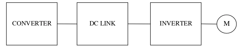
Inverters industrial applications are for adjustable frequency drives (AFDs), HVDC transmission line, uninterruptable power supply (UPS) and electric vehicles [7]. Adjustable frequency drives (AFDs) consist of converter, DC link, inverter and motor as shown in Figure 2.1. Diode rectifiers are usually used as converter to converts line AC voltage between 50Hz-60Hz to DC voltage. The DC link transmits the DC voltage to the inverter. By storing energy, it provides ride-through capability as well as some isolation from utility. Motor as the AC loads requires adjustable voltage and frequency at their input terminals. Thus, they are fed by inverters as to fulfill the requirement load.
Figure 2.1: Block diagram of adjustable frequency drive (AFD)
M
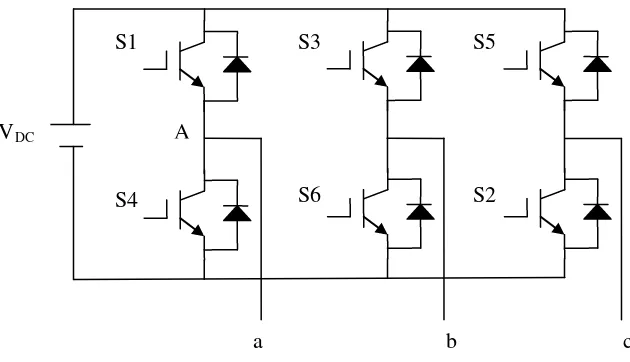
As shown in Figure 2.2, three- phase voltage source inverter (VSI) is composed with DC supply and pair of switch in each leg. Each switch is made up of fully controllable semiconductor, IGBT and diode. Upper and lower switch in each leg are complimentary in operation. If the lower switch is ON, the upper switch must be OFF in order to protect the circuit. The DC voltage at the input terminal is assumed as being constant. Symbols of (a, b, c) are donated as the inverter outputs, while (A, B, C) refer to the points connection of the outputs legs. The three-phase voltage source inverter (VSI) is developed assuming the commutation is ideal and zero forward voltage drop, six-step mode and phase delay between firing of two switches in any subsequent two phases is equal to ⁄ .
Figure 2.2: Power circuit topology of a three-phase voltage source inverter
The driving control gate for six-step mode operation of inverter in Figure 2.2 is illustrated in Figure 2.3. This driving control gate generates signal to inverter. One complete cycle is divided into six operation mode. Each of operation modes carries ⁄ . At
a b c
S1
S4
S3 S5
S6 S2