ISSN: 1532-5008 print/1532-5016 online DOI: 10.1080/15325008.2010.482092
A Simple Approach of Space-vector Pulse Width
Modulation Realization Based on Field
Programmable Gate Array
TOLE SUTIKNO,
1;2WONG JENN HWA,
1AUZANI JIDIN,
1;3and NIK RUMZI NIK IDRIS
11Department of Energy Conversion, Faculty of Electrical Engineering,
Universiti Teknologi Malaysia (UTM), Johor, Malaysia
2Department of Electrical Engineering, Faculty of Industrial Technology,
Universitas Ahmad Dahlan, Yogyakarta, Indonesia
3Department of Power Electronics and Drives, Faculty of Electrical
Engineering, Universiti Teknikal Malaysia Melaka (UTeM), Melaka, Malaysia
Abstract Employing a field programmable gate array to realize space-vector pulse width modulation is a solution to boost system performance. Although there is much literature in the application of three-phase space-vector pulse width modulation based on field programmable gate arrays, most is on conventional space-vector pulse width modulation with designs that are complicated. This article will present a simple approach to realize five-segment discontinuous space-vector pulse width modulation based on a field programmable gate array, in which the judging of sectors and the calculation of the firing time are simpler with fewer switching losses. The proposed space-vector pulse width modulation has been successfully designed and implemented to drive on a three-phase inverter system that is loaded by an induction machine of 1.5 kW using the APEX20KE Altera field programmable gate array (Altera Corpora-tion, San Jose, California, USA).
Keywords electric drives, field programmable gate array applications, motor con-trols, power converters, space-vector pulse width modulation
1.
Introduction
The space-vector pulse width modulation (SVM) method is an advanced pulse width modulation (PWM) method and is the best among all the PWM techniques in the application of variable frequency drives. SVM provides a better fundamental output voltage, better harmonic performance, and is easy to implement [1–13]. In recent years, the SVM method has gradually obtained widespread application in power electronics and electrical drives due to its superior performance characteristics. Compared with sinusoidal pulse width modulation (SPWM), SVM is more suitable for digital implementation because the obtainable DC voltage utilization ratio can highly be increased. As the
Received 26 August 2009; accepted 23 March 2010.
Address correspondence to Mr. Tole Sutikno, Department of Energy Conversion, Faculty of Electrical Engineering, Universiti Teknologi Malaysia (UTM), 81310 Skudai, Johor Bahru, Johor, Malaysia. E-mail: [email protected] or [email protected]
1546
analog and software solutions (DSP and microcontroller) [19–24], and its architecture offers a significant integration density [25] within a flexible programmable environment. Designers can get a new degree of freedom by the applying the FPGA in SVM, because the dedicated hardware architectures of the FPGA matches all of the requirements in terms of control performance as well as the implementation constraints [19]. Employ-ing the FPGA in SVM strategies provides many advantages, such as shorter design cycle, fair cost, rapid prototyping, simpler hardware and software design, and higher switching frequency. Differing with the software implementation, the FPGA performs the entire procedure with a concurrent operation (allowing parallel processing by means of a hardware mode and not occupying) by using its reconfigurable hardware. With its powerful computation ability and flexibility, an FPGA is quite mature in the application of electrical drives, and it is considerable as a solution to boost the system performance when including the SVM algorithm [6, 19, 26–29].
The digital hardware FPGA-based solution has been widely implemented in many control applications, including SVM realization [6, 19, 26–29]. However, conventional SVM suffers from drawbacks such as computational burden, inferior performance at high modulation indices, and high switching losses of the inverters. Hence, to reduce the switching losses and to improve the performance in the high-modulation region, several discontinuous SVM methods have been proposed [5, 15, 30–32].
Literature on the implementation of three-phase conventional SVM and discontinuous SVM based on the FPGA is not lacking. However, most of the designs are based on conventional SVM without consideration of the hardware-resource saving and are more complex. In this article, new approaches of FPGA-based SVM will be discussed, where the judging of sectors and the calculation of the firing time to generate the
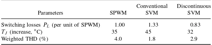
Table 1
Comparison of switching losses, temperature, and weighted THD of the different modulation schemes [15]
Parameters SPWM
Conventional SVM
Discontinuous SVM
Switching lossesPL (per unit of SPWM) 1.00 1.33 0.83
TJ (increase,ıC) 35 45 32
Weighted THD (%) 4.0 1.8 2.9
SVM waveform is simple with low switching losses and hardware-resource saving. A novel five-segment discontinuous SVM design based on the basic idea from [33] and [18] is proposed, and the scheme with lower switching losses and a simpler algorithm is implemented through the APEX20KE Altera FPGA (Altera Corporation, San Jose, California, USA).
2.
Novel Method of SVM Algorithm
The conventional principle of the SVM algorithm relies too much on the judging of sectors, and firing time (duration of active vectors) calculation and the method of switch-ing sequence generation is too complex. As a solution to overcome the problems from the conventional SVM algorithm, this article proposes the principle of a symmetrical five-segment discontinuous switching sequence that has not yet been revealed as a novel method of SVM algorithm.
2.1. Proposed SVM Switching Pattern (Five-segment Discontinuous Switching Sequence)
Many discontinuous SVM patterns have been reported [5, 6, 30, 31, 34]. However, these patterns performed with high switching losses and used a complicated algorithm that is not easily implemented based on an FPGA. In this article, a novel symmetric five-segment discontinuous SVM is proposed, the design of which mainly originated from the ideas of [33] and [18]. The pattern has been successfully implemented by Yu based on DSP [18]. This pattern resulted in lower switching losses, a simpler algorithm, and easy implementation. Therefore, this article will focus on implementation of a discontinuous SVM pattern based on an FPGA in order to boost system performance. In this proposed pattern, there is always a leg that stays constant for the entire PWM period. The state sequence in this pattern is X-Y-Z-Y-X, where Z D 1 in Sectors I, III, and V; Z D 0 in the remaining sectors. Thus, the number of switching times for this pattern is less than the conventional pattern, and the obvious result is reduced switching losses.
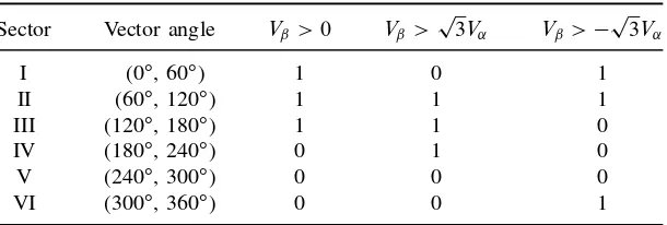
2.2. Proposed Identification of the Sector
There are many different methods to judge the sector where the reference space voltage vector lies. Zhi-pu [35] compared the reference space vector’s angle with 0ı, 60ı, 120ı, 180ı, 240ı, and 300ı to obtain the number of the sector where V
ref is Yu et al.[36],
Jianget al.[37], and Xing and Zhao [7] obtained the sector number by analyzing the relationship betweenV˛andVˇ. To determine the sector, the inverse Clark transformation
is used for the calculation of projectionsVa,Vb, andVcofV˛andVˇin the.a; b; c/-plane,
Figure 1. The plotting ofVˇ;p3V˛; p3V˛wave.
Then, based on Eq. (1),N Dsign.Va/C2sign.Vb/C4sign.Vc/, mappingN to the
actual sector of the output voltage reference by referring to the following relationship:
N 1 2 3 4 5 6
Sector II VI I IV III V
In [38], Zelianget al. adopted two new intermediate vectorsX˛ and Xˇ, whereby X˛ D 32V˛ andXˇ D
p
3Vˇ. Decomposing the conventional SVM will properly
coun-teract the redundant calculations to identify sector location, but it results in complicated matrix calculations. In this article, by analyzing on the principle of SVM in [7, 36–38] and to reduce the burden of computation, a new method to determine the sectors of voltage vectors based on a comparison betweenVˇ,
p 3V˛,
p
3V˛, and 0, as shown in Figure 1,
is proposed. Through the comparison, sectors of voltage vectors, as shown in Table 2, can be determined.
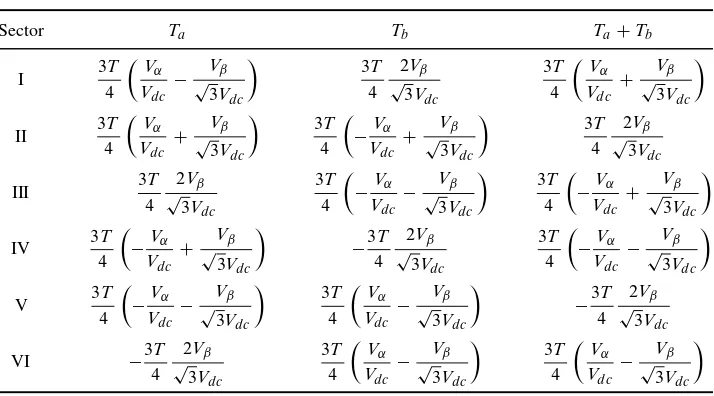
2.3. Determination of the Duration of Active Vectors
The space-vector technique synthesizes a desired vector Vref from two adjacent actives, V˛ andVˇ (amongV1andV2, as shown in Figure 1) during time intervalTaandTb. The
Table 2
Proposed identification of the sectors
Sector Vector angle Vˇ > 0 Vˇ> p
3V˛ Vˇ > p
3V˛
I (0ı, 60ı) 1 0 1
II (60ı, 120ı) 1 1 1
III (120ı, 180ı) 1 1 0
IV (180ı, 240ı) 0 1 0
V (240ı, 300ı) 0 0 0
VI (300ı, 360ı) 0 0 1
Note: 1: satisfied; 0: not satisfied.
Table 3
Switching time of the active vector for each sector
Sector Ta Tb TaCTb
null vectors (V andV7) are also applied to reduce the inverter switching frequency. In
the proposed design, only one null vector is inserted in a PWM period, wherebyV7 is
used for odd sectors andV for even sectors:
Vref DV˛CjVˇD
total time of the null vectors can be expressed as
T0D T
2 Ta Tb: (4)
In this design, the switching times of the active vectors for each sector can be calculated as shown in Table 3.
2.4. Proposed SVM Switching Sequence Generating Method Based on Calculation of the Duration of Active Vectors
In this article, a new method of SVM switching sequence is proposed, whereby the PWM signal for odd sectors are realized through comparison between the triangle waveform with Ta and TaCTb. A high signal will be generated when the triangle waveform is
higher than signal A or B, and another leg is always set to 1. For even sectors, the generation of the PWM signal is a complement to the odd sectors, whereby the signal will be set high when the triangle waveform is lower than signalAorBand another leg is set to 0.
Figure 2. Proposed SVM switching sequence generating method.
To simplify the design process, the term 2mT will set to 1 so thaty will be always equal tox(xD T0
2 DTa, thenyDxDTa; and ifxD T1
2, then y = T1
2 DTb). Obviously
ifx D T0 2 C
T1
2 D TaCTb, then yD T0
2 C T1
2 DTaCTb. Therefore, the generation of
PWM forSb andSclegs in Sector I can be obtained by comparing the triangle waveform
withTa, andTaCTb, respectively, and theSaleg is set to 1 due to the odd sector position,
as shown in Figure 2.
3.
FPGA Implementation of Proposed Novel SVM
After the discussion on the principle of SVM generation, this section focuses on the implementation of an FPGA in SVM. The overall proposed SVM design is shown in Figure 3. It can be seen from this figure that the design consists of five blocks or mod-ules, namely ajust_freq,Vbeta_Valfa,find_sector,SVM_generator, anddeadtime_sytem module. Each of these modules is explained in the following subsections.
3.1. First Module:ajust_freq
From Figure 3, the function ofajust_freqis to generate a suitable clocking frequency. In the proposed SVM design, this module functions as a frequency divider by generating a carrier frequency of 20 kHz and a fundamental frequency of 50 Hz from the FPGA board, which have a clocking signal of 33.33 Mhz. Since the triangle signal generator in this design is sampled to be 32 times per period, in order to get a carrier frequency of 20 kHz, the main clock generator from the FPGA board was divided by 13 (33.33 MHz: (1332/D20kHz).
Figure 3. Overall of the proposed SVM design.
3.2. Second Module: Vbeta_Valfa
In the proposed method,Valfa andVbetaare generated based on sine and cosine functions
through the look-up table (LUT) with a memory mapping of 360 addresses. There are three lines, categorized as lower, base, and upper, that are represented with 96, 224, and 352, respectively, into 9 unsigned bits. With the memory mapping of 360 addresses, the counter mod-360 will used to count the LUT ofValfa andVbeta.
3.3. Third Module: find_sector
Due to the different switching time equations, a reference voltage sector is necessary. The sector finder (SF) module in this design is used to judge the reference vector sector by referring to Table 2. This module determines the number of sectors and simplifies the truth table by comparing the above-mentioned results.
3.4. Fourth Module:SVM_generator
This module was divided into four sub-modules, namely Triangle, Duration_Ta,
Duration_TaTb, andSVM patternmodules. TheTrianglemodule functions as a triangle signal generator. In the proposed SVM design, one period of triangle signal generation is sampled 32 times and is represented in the digital number of 9 unsigned bits with lower (in this case, it is the same with the base number) and upper numbers of 224 and 352, respectively. TheDuration_TaandDuration_TaTbmodules are digital solutions for each second and fourth column, respectively. Finally, theSVM patternmodule is used to generate the SVM sequence as described in Section 2.4.
3.5. Fifth Module: deadtime_system
A dead-time of at least 2s is required to avoid short circuit within a leg. A combination
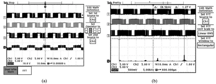
Figure 4. Hardware implementation of proposed SVM generator at carrier frequency 20 kHz: (a) the switching state and its line to line and (b) the signal gating and its frequency spectrum.
of a 16-bit counter and a 16-bit comparator is used to construct the dead-time generator for each leg.
4.
Results and Discussions
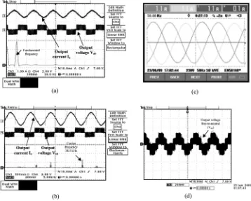
In this research, the proposed SVM generator with different carrier frequencies was successfully carried out using of the APEX20KE Altera FPGA. Figure 4 shows the results from hardware implementation with this proposed SVM generating method at carrier frequency of 20 kHz. Probes 1, 2, and 3 in Figures 4(a) and 4(b) are represented as switching states ofSa,Sb, andSc, respectively, whereby probeM is a (SaCSb)
line-to-line switching state with its frequency spectrum. The harmonics due to the 20 kHz switching frequency are clearly visible in Figure 4(b).
A similar condition is shown in Figure 5. In this case, the carrier frequency is set to 40 kHz, although the result in Figure 5(b) shows 38.5 kHz (an error of 3.75%). A
Figure 5. Hardware implementation of proposed SVM generator at carrier frequency 40 kHz: (a) the switching signals and line-to-line switching and (b) the signal gating and its frequency spectrum.
Figure 6. The performance of FPGA-based proposed SVM generator design: (a) output current and voltage, (b) frequency spectrum, (c) output threephase current, and (d) output voltage line to neutral.
three-phase inverter system together with an induction machine of 1.5 kW is used to test the performance for the proposed SVM-generator-based FPGA design.
Figure 6 shows the practical result for output stator current (Ia), output
phase-to-phase voltage (Vab), frequency spectrum, output three-phase current, and output voltage
line-to-neutral (Van). The results show that this proposed SVM-generator-based FPGA
design is successful when implemented through a hardware platform.
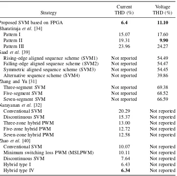
Furthermore, a comparison of current and voltage THD between the proposed SVM and other SVMs is shown in Table 4. From the table, the proposed SVM shows a lower percentage in current and voltage THD compared with other SVMs. However, the current THD from the proposed SVM (6.4%) is slightly higher than the hybrid type IV proposed by Zhao et al.[40], which is 6.34%. In addition, the voltage THD is 11.10% and is slightly higher than the pattern III proposed by Bharatirajaet al. [34] with 9.90%
5.
Conclusion
This article mainly presents the design and realization of a simple five-segment dis-continuous SVM based on the application of an FPGA. The judging of sectors and the calculation of the firing time to generate the SVM waveform become simpler, and switching losses can also be reduced by using this new approach of SVM-based
Falling-edge aligned sequence scheme (SVM2) Not reported 54.47 Symmetric aligned sequence scheme (SVM3) Not reported 54.45
Alternative sequence scheme (SVM4) Not reported 39.86
Zhang and Yu [31]
Three-segment SVM Not reported 69.38
Five-segment SVM Not reported 68.52
Seven-segment SVM Not reported 66.59
Narayanan et al.[32]
Conventional SVM 20.29 Not reported
Discontinuous SVM 15.37 Not reported
Three-zone hybrid PWM 13.00 Not reported
Five-zone hybrid PWM 12.72 Not reported
Seven-zone hybrid PWM 12.58 Not reported
Zhaoet al.[40]
Conventional SVM 10.07 Not reported
Minimum switching loss PWM (MSLPWM) 10.11 Not reported
Discontinuous SVM 7.64 Not reported
Hybrid type I 6.43 Not reported
Hybrid type IV 6.34 Not reported
FPGA. The proposed SVM scheme has been successfully designed and implemented through the APEX20KE Altera FPGA without computing the number and angles of each sector as well as the commutation pattern. A three-phase inverter system loaded by an induction machine of 1.5 kW was successfully driven by the proposed design with a carrier frequency up to 40 kHz.
References
1. van der Broeck, H. W., Skudelny, H. C., and Stanke, G. V., “Analysis and realization of a pulsewidth modulator based on voltage space vectors,”IEEE Trans. Industry Appl., Vol. 24, pp. 142–150, 1988.
2. Bose, B. K.,Modern Power Electronics and AC Drives, Upper Saddle River, NJ: Prentice-Hall PTR, 2002.
3. Holtz, J., “Pulsewidth modulation—a survey,” IEEE Trans. Industrial Electron., Vol. 39, pp. 410–420, 1992.
4. Gopinath, A., Mohamed, A. S. A., and Baiju, M. R., “Fractal based space vector PWM for multilevel inverters: A novel approach,”IEEE Trans. Industrial Electron., Vol. 56, pp. 1230– 1237, 2009.
5. Keliang, Z., and Danwei, W., “Relationship between space-vector modulation and three-phase carrier-based PWM: A comprehensive analysis [three-phase inverters],”IEEE Trans. Industrial Electron., Vol. 49, pp. 186–196, 2002.
6. Tzou, Y.-Y., and Hsu, H.-J., “FPGA realization of space-vector PWM control IC for three-phase PWM inverters,”IEEE Trans. Power Electron., Vol. 12, pp. 953–963, 1997.
7. Xing, S., and Zhao, K.-Y., “Research on a novel SVPWM algorithm,”2nd IEEE Conference on Industrial Electronics and Applications (ICIEA 2007), pp. 1869–1872, Harbin, 23–25 May 2007.
8. Deng-ke, Y., Guo-qing, X., Bo, H., An, X., and Jin-song, K., “Research on a novel SVPWM for three-phase VSI,”IEEE Vehicle Power and Propulsion Conference 2008 (VPPC ’08), pp. 1–5, Harbin, 3–5 September 2008.
9. Yinhai, Z., Songsong, W., Haixia, X., and Jinfa, G., “A novel SVPWM modulation scheme,”
Twenty-Fourth Annual IEEE Applied Power Electronics Conference and Exposition 2009 (APEC 2009), pp. 128–131, Washington, DC, 15–19 February 2009.
10. Naguib, M. F., and Lopes, L., “Minimize low-order harmonics in low-switching-frequency space-vector-modulated current source converters with minimum harmonic tracking technique,”
IEEE Trans. Power Electron., Vol. 24, pp. 881–893, 2009.
11. Lopes, L., and Naguib, M. F., “Space vector modulation for low switching frequency current source converters with reduced low-order noncharacteristic harmonics,” IEEE Trans. Power Electron., Vol. 24, pp. 903–910, 2009.
12. Casadei, D., Serra, G., and Tani, K., “Implementation of a direct control algorithm for induction motors based on discrete space vector modulation,” IEEE Trans. Power Electron., Vol. 15, pp. 769–777, 2000.
13. Bong-Hwan, K., Tae-Woo, K., and Jang-Hyoun, Y., “A novel SVM-based hysteresis current controller,”IEEE Trans. Power Electron., Vol. 13, pp. 297–307, 1998.
14. Boys, J. T., and Handley, P. G., “Harmonic analysis of space vector modulated PWM wave-forms,” IEE Proc. Elect. Power Appl. B, Vol. 137, pp. 197–204, 1990.
15. Mehrizi-Sani, A., Filizadeh, S., and Wilson, P. L., “Harmonic and loss analysis of space-vector modulated converters,” International Conference on Power Systems Transients (IPST’07), Lyon, France, 4–7 June 2007.
16. Fyntanakis, A., Adamidis, G., and Koutsogiannis, Z., “Comparison between two different methods of calculation of switching time which is used for implementation of SVPWM using DSP,” 18th International Conference on Electrical Machines 2008 (ICEM 2008), pp. 1–6, Vilamoura, 6–9 September 2008.
17. Gui-jie, Y., Li, S., Nai-zheng, C., and Yong-ping, L., “Study on method of the space vector PWM,”CSEE (China), Vol. 21, pp. 79–83, 2001.
18. Yu, Z., “Space-vector PWM with TMS320C24x/F24x using hardware and software determined switching patterns,” Texas Instruments Application Report SPRA524, March 1999.
19. Naouar, M. W., Monmasson, E., Naassani, A. A., Slama-Belkhodja, I., and Patin, N., “FPGA-based current controllers for AC machine drives—a review,”IEEE Trans. Industrial Electron., Vol. 54, pp. 1907–1925, 2007.
20. Rodriguez-Andina, J. J., Moure, M. J., and Valdes, M. D., “Features, design tools, and application domains of FPGAs,” IEEE Trans. Industrial Electron., Vol. 54, pp. 1810–1823, 2007.
21. Monmasson, E., and Cirstea, M. N., “FPGA design methodology for industrial control systems: A review,”IEEE Trans. Industrial Electron., Vol. 54, pp. 1824–1842, 2007.
22. Xuefang, L.-S., Morel, F., Llor, A. M., Allard, B., and Retif, J. M., “Implementation of hybrid control for motor drives,”IEEE Trans. Industrial Electron., Vol. 54, pp. 1946–1952, 2007. 23. Acero, J., Navarro, D., Barraga, L. A., Garde, I., Artigas, J. I., and Burdio, J. M., “FPGA-based
power measuring for induction heating appliances using sigma delta A/D conversion,”IEEE Trans. Industrial Electron., Vol. 54, pp. 1843–1852, 2007.
29. Ning-Yi, D., Man-Chung, W., Fan, N., and Ying-Duo, H., “A FPGA-based generalized pulse width modulator for three-leg center-split and four-leg voltage source inverters,”IEEE Trans. Power Electron., Vol. 23, pp. 1472–1484, 2008.
30. Gowri, K. S., Redd, T. B., and Babu, C. S., “Novel space vector based generalized discon-tinuous PWM algorithm for induction motor drives,”ARPN J. Eng. Appl. Sci., Vol. 4, No. 1, pp. 76–88, February 2009.
31. Zhang, W.-F., and Yu, Y.-H., “Comparison of three SVPWM strategis,” J. Electron. Sci. Technol. China, Vol. 5, No. 3, pp. 283–287, September 2007.
32. Narayanan, G., Zhao, D., Krishnamurthy, H. K., Ayyanar, R., and Ranganathan, V. T., “Space vector based hybrid PWM techniques for reduced current ripple,” IEEE Trans. Industrial Electron., Vol. 55, No. 4, pp. 1614–1627, April 2008.
33. Trzynadlowski, A. M., Kirlin, R. L., and Legowski, S., “Space vector PWM technique with minimum switching losses and a variable pulse rate,”Proc. IECON ’93, Vol. 2, pp. 689-694, 1993.
34. Bharatiraja, C., Prasad, T. B., and Latha, R., “Comparative realization of different SVPWM schemes in linear modulation using FPGA,”IEEE Region 8 Sibircon, pp. 164–168, Novosibirsk, 21–25 July 2008.
35. Zhi-pu, Z., “Design and realization of space vector PWM based on SG,”Drive Control, Vol. 7, pp. 29–32, 2005.
36. Yu, F., Yan, X., and Yuwen, H., “A fast algorithm for SVPWM in three phase power factor correction application,” IEEE 35th Annual Power Electronics Specialists Conference 2004 (PESC 04), Vol. 2, pp. 976–979, 2004.
37. Jiang, S., Liang, J., Liu, Y., Yamazaki, K., and Fujishima, M., “Modeling and cosimulation of FPGA-based SVPWM control for PMSM,” 31st Annual Conference of IEEE Industrial Electronics Society 2005 (IECON 2005), p. 6, Raleigh, 6–10 November 2005.
38. Zeliang, S., Jian, T., Yuhua, G., and Jisan, L., “An efficient SVPWM algorithm with low computational overhead for three-phase inverters,” IEEE Trans. Power Electron., Vol. 22, pp. 1797–1805, 2007.
39. Saad, N. H., El Meged, A., and Mahmoud, A., “Comparison of state space vector PWM schemes for a voltage source inverter,”International Conference on Computer Engineering & Systems 2008 (ICCES 2008), pp. 303–308, Cairo, 25–27 November 2008.
40. Zhao, D., Hari, V. S. S. P. K., Narayanan, G., and Ayyanar, R., “Space vector based hybrid pulse width modulation techniques for reduced harmonic distortion and switching loss,”IEEE Trans. Power Electron., Vol. 25, No. 3, pp. 760–774, March 2010.