Design of Generalized Chebyshev Lowpass Filter
with Defected Stripline Structure (DSS)
Z. Zakaria, M. A. Mutalib, M. S. M. Isa, A. A. Md Isa, N. A. Zainuddin and W. Y. Sam
Centre of Telecommunication Research and Innovation (CeTRI), Faculty of Electronic and Computer Engineering, Universiti Teknikal Malaysia Melaka (UTeM), Hang Tuah Jaya 76100, Durian Tunggal, Melaka, Malaysia
[email protected], [email protected]
Abstract—This paper presents the design of generalized Chebyshev lowpass filter (LPF) and integrated with Defected Stripline Structure (DSS) using Suspended Stripline Structure (SSS). The study involves circuit analysis to determine generalized Chebyshev responses with a transmission zero at finite frequency in order to produce a reduced number of elements values of prototype circuit. The LPF provides a cut-off frequency at 6 GHz with a return loss better than -19 dB, while the DSS exhibits a notch at frequency of 3.2 GHz with a stopband response better than -40 dB. Thus, the integrated LPF and DSS will produce lowpass and band reject response simultaneously. The design is implemented on a Roger Duroid RO4350 with a thickness of 0.168 mm and dielectric constant, of 3.48. The simulation performance results show promising results that could be proved in the experiment works. This new class of integrated LPF and DSS would be useful in any RF/ microwave communication systems particularly in wideband applications where the reduction of overall physical volume, weight and cost is critical to maintaining its good performance.
Keywords—Microwave filter; lowpass filter (LPF); bandstop filter; Defected Stripline Structure (DSS); Suspended Stripline Strucutre (SSS).
I. INTRODUCTION
With the fast development of wideband wireless communication, LPF with characteristics of high performance, low-cost, low insertion loss (IL) and compact LPF are highly desirable. For the next generation of wireless communication system, the integration of the LPF and DMS into one structure brings many benefits especially in reducing the overall physical volume of the RF systems [1]-[4]. In [5] below, the multi-band filter was presented which uses 7th degree of Chebyshev based on lowpass filter prototype. However, this paper use coupling topology method to produce multi-band filter. The DMS with band reject response has the advantages in term of good frequency selectivity, low loss and simple circuit topology [6]. The DMS is made by defect the conductor line of the structure and etching a narrow slot in the microstrip line. DMS is more easily integrated with other microwave circuits in order to reduce the size compared to DGS. In DMS, there is no etching in the ground plane and this avoids any incremental leakage through the ground plane.
Recently, DMS [6]-[8] and DGS [9][10] have been proposed in the microstrip filters. The comparison between DGS and DMS is shown in [11]. The DMS can produce
higher stopband and can apply in harmonic suppression, but the bandwidth of stopband is wider compared to the DGS. G. Yang et al. [12] introduce a wideband frequency with band reject was produced at certain frequencies. The method that they use is a meander line slot which produces a narrow notched band reject at desire frequency. However, this method cannot reach the lower frequency which provides a frequency from 4 GHz to 8 GHz. To provide a lower frequency, a longer structure is needed which increase the value of L1 to fulfill the
desired frequency. On the basis of DMS, the modified planar transmission line with the DSS is proposed which can be realized by the etching meander line slot on the signal pattern of stripline. The slot on stripline disturb current distribution on strip and grants the stopband characteristics in the frequency response [13].
In this paper, a new topology of integration between LPF and DSS is presented. The LPF is designed at a cut-off frequency of 6 GHz with minimum stopband insertion loss of 40 dB and minimum passband return loss of 20 dB. While, the DSS is designed at a frequency of 3.2 GHz with a band reject better than -40 dB with narrow bandwidth characteristics. The overall topology is designed based on SSS to produce good selectivity and low loss characteristics as well as exhibit lowpass and band reject response simultaneously.
II. DESIGN OF LOWPASS FILTER
A systematic filter design starts with a classical lowpass lumped element equivalent circuit or prototype [14]-[16]. It consists of series and shunt inductors and capacitors and their combination to form either series or parallel resonators.
The generalized Chebyshev has equiripple response in passband but with arbitrary placed transmission zeros in the stopband offering selectivity nearly as good as the same degree elliptic filter. Generalized Chebyshev filter prototype is more preferred due to the transmission zeros can be placed independently as accordance to design specification. Alseyab in [17] synthesize the element values for generalized Chebyshev low pass filter prototype which can be used to transform into any filter response. The doubly terminated low-pass prototype network satisfies the insertion-loss (IL) for the generalized Chebyshev response as described by:
IL cosh N cosh ω ωω
cosh ω
where the transmission zeros are of order ( and one at infinity. N is an odd number equa the network,
RL⁄ /
and RL is the minimum return loss level (dB
A. Design of Lowpass Filter
The device is constructed and simulated Duroid RO4350 with relative dielectric co substrate height, h = 0.168 mm. the thicknes mm and the loss tangent is 0.019. The frequency of 6 GHz with the degree, N = stopband insertion loss of -40 dB and m return loss of -20 dB are designed based on and (2). The elements values for the lowpass show in Table 1 with its correspon
. / can be obtained in [17].
The lowpass prototype operates in system and cut-off frequency of 1 rad/s. The next ste transformation to lowpass filter with 50 Ω prototype using following equations [18]:
By implementing Equation (3) and (4), value and inductors that operating in 50 Ω with cut-GHz can be calculated.
The element values of the equivalent c filter are shown in Table 2. The lowpass filt be seen in Fig. 1(a). The response of the shown in Fig. 1(b). It is observed that the f frequency of 6 GHz which are in line specification. LPF with cut-off = 7, the minimum minimum passband calculations in (1) prototype network nding
UMPED ELEMENTS
2 7
impedance of 1Ω ep is to perform the
from the lowpass
(3)
(4)
s of each capacitor -off frequency of 6
ircuit for lowpass ter circuit can now e lowpass filter is filter has a cut-off
with the design
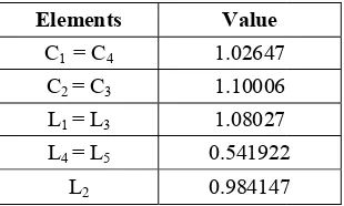
TABLE 2:COMPONENT VA Fig. 1. (a) Seventh-degree generalized (b) Simulated frequency response of th
B. Physical Realization
For realization, the lumped transformed to open- and s segments by applying Richard’
The Richard’s transformat inductors with short circu impedance and capacit characteristic impedance can be represented as admittan characteristic admittance ⁄
The length of the stub is Constant can be obtai transformation at the band-edge
and
d Chebyshev lowpass prototype network he generalized Chebyshev lowpass filter
d element lowpass filter is then short-circuit transmission line ’s transformation [16].
tion allows to replace lumped uited stubs of characteristic
tors with open circuited stubs of
⁄ . The resonator impedance nce of an open circuited stub by
.
one quarter wavelength at . ined by applying Richard’s
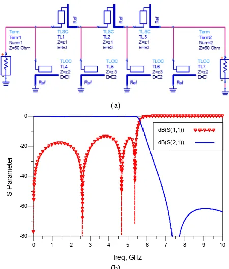
The structure of distributed element af Richard’s transformation is shown in Fig. 2 short- and open-circuit stubs are shown in Ta
TABLE 3:ELEMENT VALUE OF STUB EL
Elements Value (Ω) Elements
z1 120 E1 z2 29.78 E2 z3 55.55 E3
The simulated results in Fig. 2 (b) show (S21) is almost 0 and the return loss (S11) bett obtained in the passband.
(a)
(b)
Fig. 2. (a) Generalized Chebyshev lowpass distributed frequency response of the generalized Chebyshev lowp
C. Suspended Stripline Structure (SSS)
Fig. 3 : Suspended Stripline Structu
This LPF is then fabricated using SSS (a in order to improve the overall filter p impedance of the SSS which is base Electromagnetic (TEM) transmission line is capacitance to ground per unit length as the f
1 2 3 4 5 6 7
0 -60 -40 -20
-80 0
freq, GHz
S-Pa
ra
m
e
te
r
dB(S
dB(S
fter applying the (a). The values of able 3.
LEMENT
Value (θ)
29.13 72.0 29.9
w an insertion loss ter than -18 dB are
d filter (b) Simulated wpass distributed filter
ure
as shown in Fig. 3) performance. The ed on Tranverse related to its static following [18]:
(7)
where is the dielectric cons the normalized static capaci transmission line. If a transm normalized static capacitan capacitance.
and
where is ground plane spaci conductor. For a printed circuit
Therefore the line width of the
where b is a ground plan characteristics of impedance lin 7th open-circuit stub can be calc
where / and
The length of the remaining op times from the equation (12). T set to 120 Ω impedance tran fabrication. Hence, the length stubs are calculated using:
si ,
= element value of the comp
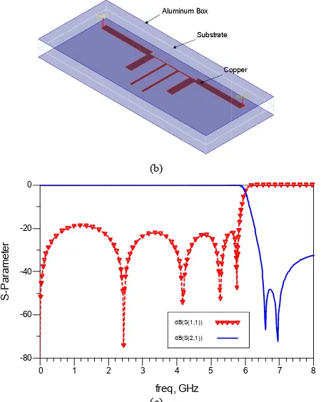
The SSS lowpass is mod using ADS Momentum as sh simulated response is shown results show in Fig. 4 (c) inse and return loss (S11) better passband.
(
8 9 10
S(1,1))
S(2,1))
stant of the medium and is tance per unit length of the mission line is suspended, the nce would include fringing
(8)
⁄ (9)
ng and is the thickness of the t, t is assumed as zero and hence
. (10)
stub, can be obtained as:
. (11)
ne spacing in mm and ne. The length, of the 1st and culated using:
(12)
pen-circuit stub resonator is two The series short-circuit stubs are nsmission line for the ease of h, of the series short-circuit
in (13)
ponent
deled, simulated and optimized hown in Fig. 4 (a) and the in Fig. 4 (b). The simulated ertion loss (S21) is almost 0 dB -18 dB are obtained in the
(b)
(c)
Fig. 4 : (a) Layout of generalized Chebyshev lowpass Generalize Chebyshev lowpass filter (c) Simulated freq generalized Chebyshev lowpass filter in suspended
The filter is manufactured on roge dielectric constant, . and thickness t=0.168 mm. The filter is then built bas stripline structure (SSS) using aluminium a (a) and (b). The roger substrate is suspended and lid of the aluminium block. The simula and return loss performances of the filter are 5 (c), and compared with measured results. the Fig. 5 (c), a good agreement between the simulated results has been obtained. The me that a cut-off frequency at 6.2 GHz is achie loss (S21) is almost 0.3 dB and return loss (S dB are obtained in the passband.
(a)
1 2 3 4 5
0 -60 -40 -20
-80 0
freq, GHz
S-Pa
ra
m
e
te
r
dB(S(1,1)) dB(S(2,1))
filter (b) 3-D view of quency response of the d stripline structure
er substrate with s of the substrate, sed on suspended as shown in Fig. 5
d between the base ated insertion loss e presented in Fig. As can seen from e measured and the easurement shows ved with insertion S11) better than -15
(
( Fig. 5 : Photograph of suspended strip
(base – without lid) (b) overall filt simulation and m
III. DEFECTED STRIP
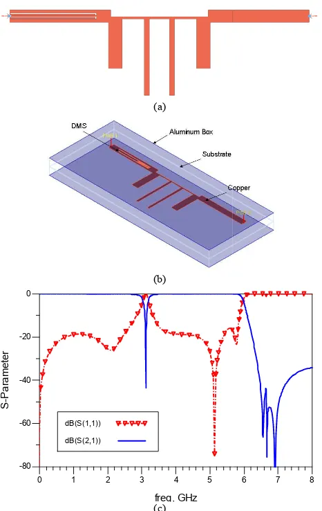
The DSS structure is prod conductor layout and it cons vertical slot [6]. As well as increases the electrical length the current distribution. With the filter size can be reduced problems compare with DGS through the ground plane [7]. integrate with other microwave In this study, the DSS is des with length, and width, conductor line. The shape of th slot which can produce a narro time the whole circuit area wi the meander line slot of DS simulated results. The results s at 3.2 GHz with narrow bandw of narrow band notch respo undesired signal in wideband DSS will be integrated with l exhibit bandpass and band reje The layout for integrated shown in Fig. 7 (a). Fig. 7 (b) integrated of the DSS and lowp that the response produces a passband of the low pass filter.
6 7 8
(b)
(c)
pline structure lowpass filter (a) inside ter structure with lid (c) comparison measurement result.
PLINE STRUCTURE (DSS) duced by etching a slot in the
sists of horizontal slot and a the DGS structure, the DSS of the microstrip and disturbs this electric length increment, d. This DSS has no enclosure S because there is no leakage Moreover, the DSS is easier to e circuits.
signed based on rectangular slot etched in the middle of the he DSS is called a meander line
w notched band and at the same ill be reduced. Fig. 6 (a) shows SS and Fig. 6 (b) shows the
show the notch response occurs width. Thus, the characteristics onse will help to remove the
applications. In this study, the lowpass filter based on SSS to
(a)
(b)
Fig. 6 : (a) Meander line slot, Ls1=10.7, Ws1=1.5, Ws Ws4=0.5, all in mm. (b) Simulated S-parameter of th
(a)
(b)
(c)
Fig. 7. (a) Structure 1 of integration between DSS and Generalize Chebyshev lowpass filter integrate with DS of integration DSS and LPF
1 2 3 4
s2=0.3, Ws3=0.1 and he meander line slot
d LPF (b) 3-D view of S (c) Simulation result
IV. CO
A new technique for the in filter has been presented. The E and excellent results. Thus the and validated by developing th and lowpass filters based on S of the integrated DSS and low and band reject response sim would be useful in microwave the reduction of overall phys important such as in a wideban
ACKNOWL
The authors would like to t work under the shor PJP/2012/FKEKK(11C)/S0101
REFER [1] Z. Zakaria, M. A. Mutalib, K Othman, B. H. Ahmad, M. Z. A Developments of Microwave
World Applied Sciences Journal
[2] Z. Zakaria, I. C. Hunter, and Resonator Filter with Nonu
International Microwave Sympo
[3] Z. Zakaria, and B. H. Ahmad. “ dB Offset,” IEEE RF and Mic
2011.
[4] Z. Zakaria, A. Sabah, W. Y. Sam Bandpass Filter with Post-Man
Symposium on Business, Eng (ISBEIA), pp. 733 – 736, 2012. [5] S. Bila, R. J. Cameron, P. Lenoi Synthesis for Multi-Band Micr
Digest, 2006. IEEE MTT-S Inter
[6] J. Xiao and W. Zhu, “New D Filter,” in Progress In Ele Proceedings, 2011, vol. 01, pp. [7] R. Sinhga and T. Moyra, “Des
Lowpass Filter by using D
International Conference on Co Systems (CODIS), vol. 1, pp. 52 [8] A. R. Mallahzadeh, B. Rahmat A. H. Ghasemi, “Ultra Wide Microstrip Structures,” 2012 6 and Propagation (EUCAP), pp. [9] F. Bahmani, J. Ourinia, C. Gh Applied to Design Lowpass F
2011 19th Iranian Conference, v [10] Z. Zakaria, N. A. Shairi, R. S
Reconfigurable Defected Gr Application,” 2012 IEEE A Electromagnetics (APACE), vol [11] J. A. Tirado-mendez and H. Ja Ground Structure (DGS) and Behavior at High Frequen
Engineering, 2004. (ICEEE). 1
2004.
[12] G. Yang, S. Member, R. Jin, C “Small Ultra-Wideband (UWB)
IEEE Microwave and Wireless
176–178, 2008.
[13] G. Chaudhary, P. Kim, Y. Jeo Circuit Modeling Method for D Transmission Lines,” Proceed Conference, 2011, pp. 999-1002
5 6
6 7 8
ONCLUSION
ntegration of DSS and lowpass EM simulation shows promising e study can be further explored he prototype of integrated DSS SSS technology. This new class wpass filter to produce lowpass multaneously in a single device e communication systems where sical volume and cost is very nd applications.
LEDGMENT
thank UTeM for sponsoring this rt term grant, UTeM, 15.
RENCES
K. Jusoff, M. S. Mohamad Isa, M. A. A. Abd. Aziz, and S. Suhaimi, “Current Filters for Wideband Applications,”
l, vol. 21, pp. 31–40, 2013.
d A. C. Guyette, “Design of Coaxial uniform Dissipation,” IEEE MTT-S osium Digest, pp. 623–626, 2008.
“Design of SIW Bandpass Filter with 6
crowave Conference (RFM), pp.87-90, m. “Design of Low-Loss Coaxial Cavity nufacturing Tuning Capabilities,” IEEE gineering and Industrial Applications
ir, V. Lunot, and F. Seyfert, “Chebyshev rowave Filters,” Microwave Symposium
rnational, pp. 1221–1224, 2006. Defected Microstrip Structure Bandstop
ectromagnetics Research Symposium
1471–1474.
sign and Performance Improvement of Defected Microstrip Structure,” 2012 ommunications, Devices and Intelligent
0–523, Dec. 2012.
ti, M. Alamolhoda, R. Sharifzadeh, and Stop Band LPF with Using Defected
6th European Conference on Antennas
1–3, Mar. 2012.
hobadi, and S. Pirani, “A Novel DGS Filter,” Electrical Engineering (ICEE),
vol. 1, pp. 5–9, 2011.
Sulaiman, and W. Y. Sam, “Design of round Structure (DGS) for UWB
Asia-Pacific Conference on Applied
l. 2, pp. 195–198, Dec. 2012.
ardon-aguilar, “Comparison of Defected Defected Microstrip Structure (DGS) ncies,” Electrical and Electronics 1st International Conference, pp. 7–10,
. Vittoria, V. G. Harris, and N. X. Sun, ) Bandpass FilterWith Notched Band,”
Components Letters, vol. 18, no. 3, pp. ong, J. Lim and J. Lee, “Analysis and Defected Microstrip Structure in Planar
dings of the Asia-Pacific Microwave
[14] Z. Zakaria, I. C. Hunter, and A. C. Guyette, “Design of Coaxial Resonator Filter with Nonuniform Dissipation,” in 2008 IEEE MTT-S International Microwave Symposium Digest, 2008, pp. 623–626. [15] Z. Zakaria, W. Y. Sam, MZ Abd Aziz, M Muzafar Ismail, “The
Integration of Rectangular SIW Filter and Microstrip Patch Antenna based on Cascaded Approach”, Procedia Engineering, Elsevier, vol. 53, pp 347-353, 2013.
[16] N. A. Shairi, B. H. Ahmad, P. W. Wong and Z. Zakaria, “Single Switchable Open Stub Resonator in SPDT Switch Design”, 2012 IEEE Symposium on Wireless Technology & Applications (ISWTA 2012),
Bandung, Indonesia, Sept. 23 – 26, 2012.
[17] S. A. Alseyab, “A Novel Class of Generalized Chebyshev Low-Pass Prototype for Suspended Substrate Stripline Filters,” IEEE Transactions on Microwave Theory and Techniques, vol. 30, no. 9, pp. 1341–1347, 1982.