1312703-1305-9494-IJECS-IJENS © October 2013 IJENS I J E N S
M. I. Idris
1, Faiz Arith
2, S. A. M. Chachuli
3,
H. H. M. Yusof
4and M.M. Ismail
51,2,3,4,5
Faculty of Electronics & Computer Engineering, Universiti Teknikal Malaysia Melaka, Hang Tuah Jaya, 76100 Durian Tunggal, Melaka, Malaysia
Abstract
--
This paper reportsthe studies on the inversion-layer mobility in n-channel Poly-Si TFT’s with 1016cm-3 substrate impurity concentration. The validity and limitations of the universal relationship between the inversion layer mobility and the effective normal field (Eeff) was examined.Index Term
–
TFT, Grain boundaries, carrier mobility, polysiliconI. INTRODUCTION
It is strongly required to understand the inversion –
layer mobility from modeling viewpoint for accurate device simulation, as well as from two-dimensional physics viewpoint. Though a qualitative understanding has already been obtained within moderate device parameters, it is indispensable to establish an accurate mobility model in a wide range of device parameters for realizing future ULSI's. Furthermore, the characterization of mobility degradation is important, in order to predict the performance of Poly-Si TFT's degraded by electric stress and others like trap, de-trap and surface roughness scattering.
On the other hand, it has already been reported that electron and hole mobilities in the inversion-layer follow universal curves, independent of the substrate impurity concentration, when plotted as a function of effective normal field [1]-[3].This relationship provides a simple guideline, which gives mobility values under a combination of various device parameters.
This paper reports results of mobility behaviors in
n-channel Poly-Si TFT's with 1016 cm-3 substrate impurity
concentration . Also, the mobility degradation by phonon scattering was studied. From these experimental results, the validity and limitations of the universal relationship have been examined.
II. SAMPLE PREPARATION AND MEASUREMENT
The n-channel Poly-Si used in this study was fabricated on (100)Si wafer. The substrate impurity
concentration is 1016cm-3 and the gate oxide’s thickness is
30nm. The measured devices had 1um gate lengths and 100um
gate widths. The carrier mobility μeff was determined from the
drain conductance gD for the Poly-Si TFT in the linear
region(VD =50mV).
(1)
Where,
(2)
and
⁄
(3)
In order to determine μeff accurately, the inversion
carrier density Ns(VG) must be measured with a minimal
measurement error. Ns(VG)was therefore ,determined directly
through gate-channel capacitance Cgc (VG) measurement[4-5].
∫
(4)
Here, the measurement frequency was 300kHz (depend on the type of device), which enable to measure capacitance values accurately, even near the threshold
voltage[5]. The effective normal field , Eeff ,was defined by
the following equation.
(5)
where Ndpl = (4 Є SiNsubфb/q)/1/2is the bulk surface charge
density. Nsub is the substrate impurity concentration, and фb is
the bulk Fermi energy. Here, η=1/2 for electron mobility was used, following previous reports [1]-[3].
Universal Mobility
-
Field Curves For Electrons
1312703-1305-9494-IJECS-IJENS © October 2013 IJENS I J E N S
III. EXPERIMENTAL RESULT AND DISCUSSION
3.1 I-V Measurent Result
I
d
-
V
d
0.00E+00 1.00E-03 2.00E-03 3.00E-03 4.00E-03 5.00E-03 6.00E-03 7.00E-03 8.00E-03 9.00E-03
0 0.5 1 1.5 2 2.5
V
d
(V)
I
d
(A
)
0 2 10-5 4 10-5 6 10-5 8 10-5 0.0001 0.00012
0 0.5 1 1.5 2 2.5 3 3.5 4
g
m
-
V
gg m
(S
)
V
g(V)
0 5 10-5 0.0001 0.00015 0.0002 0.00025 0.0003 0.00035
0 1 2 3 4 5 6 7
I
d
-
V
gI d
(A
)
V
[image:2.612.310.513.118.318.2]g(V)
Fig.. 1. Measured drain current versus gate voltage. Fig. 2. Measured gm versus gate voltage and the way how threshold voltage was
[image:2.612.32.233.120.319.2]determined.
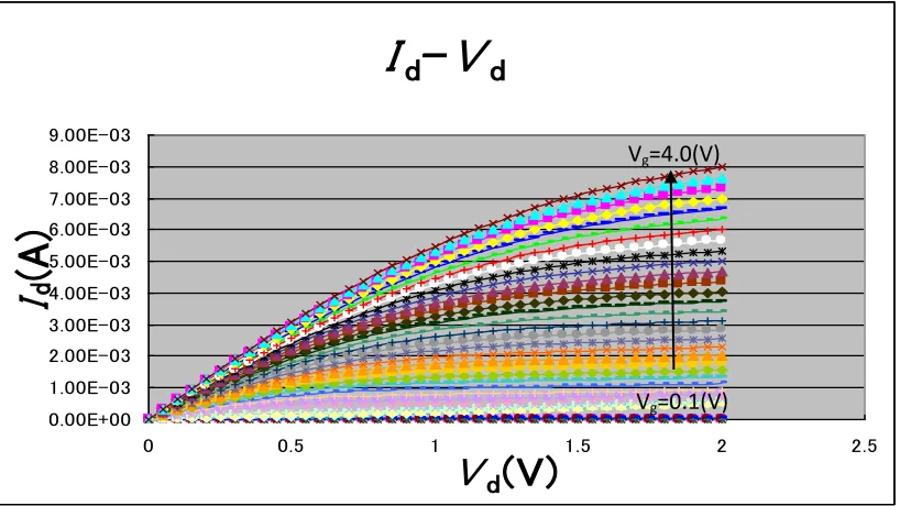
Fig.. 3. Measured drain current versus drain voltage as a parameter of gate voltage.
V
g=4.0(V)
[image:2.612.103.512.356.586.2]1312703-1305-9494-IJECS-IJENS © October 2013 IJENS I J E N S
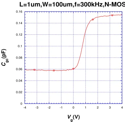
3.2 C-V Measurement
g
d
-
V
d
0.00E+00 1.00E-03 2.00E-03 3.00E-03 4.00E-03 5.00E-03 6.00E-03 7.00E-03
0 0.5 1 1.5 2 2.5
V
d
(A)
g
d
Fig. 4. Measured gD versus drain voltage as a parameter of gate voltage.
0 0.02 0.04 0.06 0.08 0.1 0.12 0.14 0.16
-4 -3 -2 -1 0 1 2 3 4
L=1um,W=100um,f=300kHz,N-MOS
C gc
(pF)
Vg(V)
1312703-1305-9494-IJECS-IJENS © October 2013 IJENS I J E N S
0.1 1 10 100 1000
0.36 0.38 0.4 0.42 0.44 0.46 0.48
É
-
E
eff
É
(cm
2
/V
s
e
c
)
E
eff
(MV/cm)
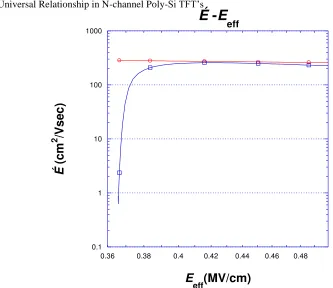
3.3 Universal Relationship in N-channel Poly-Si TFT’s
0 5 10-8 1 10-7 1.5 10-7 2 10-7 2.5 10-7 3 10-7 3.5 10-7 4 10-7
0 1 2 3 4 5
Q
N-
V
gQ
N
(
c
o
u
l/c
m
2 )
V
g
(V)
10-9 10-8 10-7 10-6
0 1 2 3 4 5
Q
N-
V
gQ N
(
co
u
l/c
m
2 )
V
[image:4.612.295.479.61.350.2]g
(V)
[image:4.612.43.232.66.355.2]Fig.. 6. Calculated (blue line) and measured (red line) channel charge versus gate voltage is plotted on a linear scale.
[image:4.612.84.417.412.700.2]Fig. 7. Calculated (blue line) and measured (red line) channel charge versus gate voltage is plotted on a logarithmic scale.
1312703-1305-9494-IJECS-IJENS © October 2013 IJENS I J E N S
Figure 8 shows the Eeff dependence of the
inversion-electron mobility at about 300K(room
temperature). It should be notice concerning electron
mobility in Figure 8 that the Eeff dependence of electron
mobility is in proportion to Eeff -0.3 at Eeff from 0.4(MV/cm)
to 0.45(MV/cm),over the one order of magnitude Eeff range.
But electron mobility starts to decrease steeply at Eeff higher
than 0.45(MV/cm),though the universality is maintained. Besides, the electron mobility value is degraded to a single figures lower than MOSFET’s mobility.
As is well known, the dominant scattering mechanism in the Si inversion-layer is phonon scattering at
high temperature and surface roughness at low temperature and high normal field. Therefore, it can be considered that
the mobility which has Eeff-0.3 dependence in figure is
limited by phonon scattering [6] and also if Eeff higher than
0.45(MV/cm) the mobility value starts to decrease steeply .Hence , the significant decrease in mobility is thought to be caused by surface roughness scattering[7]. But in Poly-Si TFT, the effect by surface roughness is faster because of the grain- boundaries in channel region. This is also can be explained by electrons trap and de-trap phenomenon(Figure 9).
IV. CONCLUSION
This paper reports the studies on the inversion-layer mobility behaviors in n-channel Poly-Si TFT’s, from the universal relationship viewpoint. A significant mobility lowering has been observed at
low Ns(low effective field), which is due to Coulomb
scattering /screen effect. Also, in n-channel Poly-Si TFT’s the significant decrease in mobility is thought to be caused by surface roughness scattering which is faster because of the grain- boundaries in channel region. Besides, the degradation of carrier-mobility in
Poly-Si TFT’s has been found. This is thought to be
caused by grain-boundaries.
From these facts, it can be concluded that, by adding the term of surface roughness and Coulomb scattering to the universal curves, a more accurate description of inversion-layer motilities can be realized.
REFERENCES
[1] A.G.Sabnis and J.TClemens, Charaterization of the electron mobility in the weakly inverted (100)silicon surface, IEDM Technical Digest,p.18(1979)
[2] N.D.Arora and G.S.Gildenblat, A semi-empirical model of the MOSFET inversion layer mobility for low temperature operation, IEEE Trans.ED, vol.ED-34,p.89(1987)
[3] J.T.Watt and J.D.Plummer, Universal mobility-field curves for electrons and holes in MOS inversion layers,
Proc.Symp.VLSI Technol., p.81(1987)
[4] C.G.Sodini, T.WEkstedt and J.L.Moll, Charge accumulation and mobility in thin dielectric MOS transistors, Solid-State Electron,vol.25,p.833(1982) [5] P.D.Chow and K.Wang, A new AC technique for
accurate determination of channel charge and mobility in very thin gate MOSFET’s, IEEE Trans.ED,vol.ED-33, p.1299(1986)
[6] S.Kawajiri, The two-dimensional lattice scattering mobility in a semiconductor inversion layer,
J.Phys.Soc.Japan ., vol.27, p.906(1969)
[7] Y.C.Cheng and E.A.Sullivan, On the role of scattering by surface roughness in silicon inversion layer,