Screen-Printed Ceramic Based MEMS Piezoelectric Cantilever for
Harvesting Energy
Swee-Leong, Kok
1,a*, Abdul Rani Othman
2,band Azizah Shaaban
3,c1,2Faculty of Electronic and Computer Engineering, Universiti Teknikal Malaysia Melaka, 76100 Melaka, Malaysia
3Faculty of Manufacturing Engineering, Universiti Teknikal Malaysia Melaka, 76100 Melaka, Malaysia
a [email protected], b [email protected], c [email protected]
Keywords: Piezoelectric, Lead Zirconate Titanate (PZT), Thick-Film Screen-Printing Technology,
Free-Standing
Abstract. Screen-printing technology provides a convenient method in fabricating thick-film conductive circuits and devices in the past few decades. Conventionally, piezoelectric thick-film is printed on alumina substrate with high mechanical Q-factor and resonates at higher frequency outside the range of ambient vibration. As the piezoelectric charge generation is proportional to the mechanical stress on the material, therefore the substrate can be removed in order to lower the natural frequency of the structure. In this paper, a series of piezoelectric ceramic cantilevers were fabricated in the form of free-standing cantilever. An additional layer of ceramic was also introduced to the upper and lower electrode to prevent delamination. The issue of zero resultant stress for the sandwiched piezoelectric cantilever was solved by repeating the electrode-PZT-electrode layer to form a multilayer structure. It was found from the experiment that an electrical output power of 32 µW was generated when it operates at its resonant frequency at 403 Hz.
Introduction
Screen printing technology in electronic applications has been evolved from simple conductive connection in a printed circuit board a few decades ago [1] to recent fabricated as MEMS hybrid sensors [2] and electronic devices for harvesting energy [3]. It has found new applications in wearable textiles [4] and fabric [5]. The enabling technology for high performance energy harvesting applications is the advancement of piezoelectric materials and fabrication techniques. So far, lead zirconate titanate (PZT) is one of the popular materials [6], although other lead-free materials [7, 8, 9] were also being reported to replace PZT but their performance were still discouraging compared to PZT especially for the application of energy harvesting [10].
In this paper, thick-film piezoelectric material PZT is used to fabricate a series of vibration based energy harvesters in the form of a cantilever. After the PZT was screen-printed, it would then be co-fired together with the electrodes at a temperature similar to low temperature co-co-fired ceramic (LTCC) processes at around 850 °C [11]. Alumina which has a thermal expansion coefficient of 8 ×10⁻⁶/°C compatible with PZT thick-film processing is being used as substrate. This alumina
substrate is also acting as a mechanical support to the thick-film piezoelectric structure when operating as a cantilever.
In order to be effective supporting structure for a fragile thick-film, alumina substrate has to be many time thicker than the thick-film itself. Thick alumina substrate, however, has high Q-factor, hence higher natural frequency. Resonance based energy harvesting device is desired to operate at frequencies match to the ambient vibration which occurs in the range far below 1 kHz, for instance, operating machinery frequency is between 50 Hz to 200 Hz and moving vehicle is between 100 Hz to 250 Hz [12].
Advances in Science and Technology Vol. 90 (2014) pp 84-92 Submitted: 08.05.2014 Online available since 2014/Oct/31 at www.scientific.net Accepted: 04.07.2014 © (2014) Trans Tech Publications, Switzerland
doi:10.4028/www.scientific.net/AST.90.84
The natural frequency of a thick-film piezoelectric cantilever with alumina supporting substrate can be drastically reduced to match the ambient vibration frequencies with a proof mass, usually tungsten, attached at the tip of the cantilever. The addition of the proof mass, however, increases the overall size of the energy harvesting device, which is not desirable for MEMS and integration of microelectronic circuits. Therefore, piezoelectric cantilever is desirable to do without the alumina supporting structure. This can be done by releasing the piezoelectric thick-film from the alumina substrate using carbon sacrificial technique.
The part of a piezoelectric thick-film structure which released from an alumina substrate is termed “free-standing structure” in this paper and has been reported in previous work in [13]. Due to the fact that ceramic is fragile and easily break, especially when it is made into thick-film with thickness less than 100 µm. A free-standing piezoelectric ceramic on its own without strong mechanical supporting structure is difficult to withstand harsh fabrication environment with strong blow of air curtain during co-firing process in a multi-zone furnace, let alone operating to its resonant frequency at random environment vibration acceleration level, which sometime can be greater than a few g-levels (1 g = 9.81 m/s2).
Design Consideration
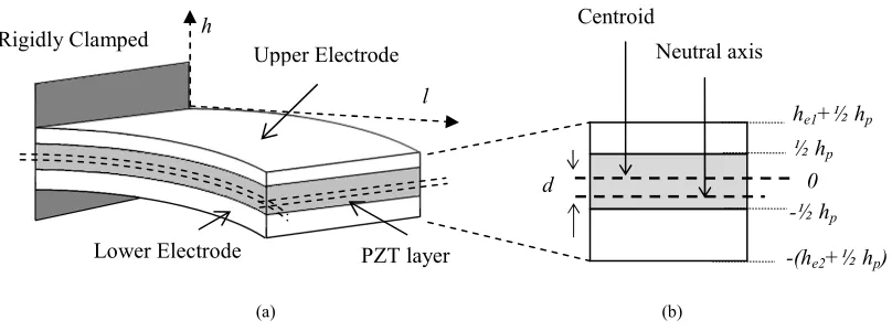
One of the factors that influence the generation of piezoelectric charge is the distance of the neutral axis of “active piezoelectric layer” from the centroid of the whole cantilever structure, d as shown in Fig.1 (b). The “active piezoelectric layer” here means the layer of thick-film piezoelectric material fabricated in the form of sandwiched structure with conductive material deposited on the upper and lower layer acting as electrodes or terminals as shown in Fig.1 (a) and has been polarized with dc voltage at elevated temperature near to its Curie temperature.
The output voltage for a piezoelectric cantilever can be estimated with [14],
. (1)
where j is the imaginary number, ωr is the resonant frequency of the cantilever, eT is the elastic constant for the composite structure (N/m2), d
31 is the piezoelectric charge coefficient (C/N), hP is the thickness of the piezoelectric material, ε is the dielectric constant of the piezoelectric material (F), ζT is the total damping ratio, k31 is the piezoelectric coupling factor, CP is the capacitance of the piezoelectric material, R is the resistive load, and d is the distance from the centroid of the layer of PZT to the neutral axis of the structure.
A bending beam or cantilever is subjected to tension and compression proportional to the distance above and below the neutral axis respectively. For a thick-film printed-on-substrate device as shown in Fig. 1(a), the thickness of the alumina substrate is usually 10 times greater than that of the active piezoelectric layer therefore the distance between the neutral axis and the centroid of the cantilever structure are about half of the thickness of alumina substrate, hAlumina as shown in Fig. 1 (b).
For a electrode-PZT-electrode cantilever structure which is without the alumina substrate as shown in Fig. 2(a), the distance, d is depended on the thickness difference between the upper and lower electrode. If both the thickness of upper and lower electrodes are similar, the neutral axis coincided with the centroid of the cantilever structure, there the resultant stress, σ acting on the piezoelectric material will be zero as shown in equation (2),
. (2)
where σ is the stress along the thickness direction, h of the multilayer structure from the neutral axis. e is the elastic modulus and κ is the curvature and the distance from the neutral axis which is nonzero. As the resultant stress on the piezoelectric material is zero therefore according to piezoelectric constitutive equation, no electrical charge will be generated.
In order to maximize the output voltage for a electrode-PZT-electrode cantilever structure, the d -distance need to be increased which can be derived as,
. (3)
where he1 and he2 are the thickness upper and lower electrode respectively, while nsp is the elastic modulus ratio of electrode and PZT layer.
Fig. 1(a) Cantilever structure with unimorph layer of piezoelectric deposited on the top surface of alumina substrate. (b) Indication of distance between centroid of the cantilever structure and neutral axis of the PZT
layer.
Fig. 2(a) Sandwiched layer of a piezoelectric cantilever structure (not according to actual scale). (b) Indication of a gap, d between centroid and neutral axis on piezoelectric layer.
Fabrication
In order to release the thick-film piezoelectric from the alumina substrate, a layer of sacrificial material would be deposited before the sandwiched structure of electrode-PZT-electrode. This sacrificial layer would be totally burnt out in the air during the process of co-firing of the piezoelectric ceramic. Carbon paste was chosen because it burnt at temperature above 800 °C [15]
and is therefore compatible to the piezoelectric ceramic sintering temperature.
l
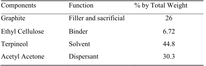
The composition of carbon paste is shown in Table 1. The main ingredients of the carbon paste are graphite powders (Sigma-Aldrich 28, 286-3), ethyl cellulose (Sigma-Aldrich 43, 383-7) as the binder and acetyl acetone (Sigma-Aldrich P775-4) as the dispersant. Firstly, ethyl cellulose was dissolved in terpineol (Fluke 86480) at 87 °C for 10 minutes, with a ratio of 15:100 by weight. The graphite power was then gradually added to the mixture, together with acetyl acetone. The resultant was made up of functional element and binder at a ratio of 28:72 (by weight).
Table 1: Carbon sacrificial layer paste composition.
Components Function % by Total Weight
Graphite Filler and sacrificial 26
Ethyl Cellulose Binder 6.72
Terpineol Solvent 44.8
Acetyl Acetone Dispersant 30.3
The main ingredient for the thick-film piezoelectric ceramic pastes are PZT powder, high temperature permanent binder, low temperature temporary binder and solvent similar to those reported in [16]. The PZT powders need to be sintered at a temperature higher than 800 °C in order
to produce high piezoelectric activity material. Lead borosilicate glass is used as the permanent binder. During the co-firing process the glass melts and binds the PZT particles together and later forms solid composite films once cooled down to a lower temperature. The presence of glass modifies the mechanical properties as well as the piezoelectric properties of the film, therefore, it is important to mix PZT powder and glass frit in correct proportions. Terpineol or pine oil is used as the temporary binders to make thixotropic pastes, which can easily pass through the printing screen. They also serve to hold the paste together during the drying process, and are eventually evaporated during the firing stage.
Table 2 shows the components of PZT paste formulation. Each of the components is expressed as a percentage of the total weight of the paste. Pz29 from Ferroperm Piezoceramics Ltd, which is compatible to PZT-5H from Morgan Electro Ceramics Ltd in terms of mechanical, electrical and electro-mechanical properties was used in formulating the pastes. Two particle sizes of PZT; 2 µm and 0.8 µm, were used in order to increase the density of the thick-film, which made up 76 % of the total weight of the paste. 4 wt.% of lead borosilicate glass (Ferroperm CF 7575) was used as the permanent binder and 20 wt.% of terpineol solvent (ESL 400) was used as the temporary binder. All of the components were mixed together and homogenized with a triple roll mill.
Table 2: PZT paste composition.
Components Function % by Total Weight
PZT* (2 µm) Active Component 60.8
PZT* (0.8 µm) Active Component 15.2
Lead Borosilicate Glass Permanent Binder 4
Terpineol Solvent Temporary Binder 20
PZT* = PZT-5H [17] or Pz 29 [18]
Fabrication Results
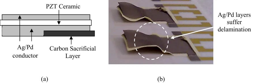
The sandwiched structure of electrode-PZT-electrode as shown in Fig. 2(a) was fabricated by screen-printed carbon sacrificial layer first before lower electrode and followed by piezoelectric ceramic paste and lastly the upper electrode as shown in Fig. 3(a). Here silver palladium (Ag/Pd) paste was being used as the material for both the lower and upper electrodes.
As a result of co-firing with peak temperature of 850 °C and holding time for 10 minutes, the upper and lower layer of Ag/Pd conductors suffer warping effect and holds loosely above and below the surface of the ceramics as can be seen in Fig. 3(b). This is due to different thermal expansion coefficient between the materials, therefore lower electrodes tend to pull the structures down while the upper layers pulled the structure the opposite position resulting in delamination.
Fig. 3 (a) Schematic (not actual scale) and (b) fabrication outcome, of a sandwiched layer of electrode-PZT-electrode.
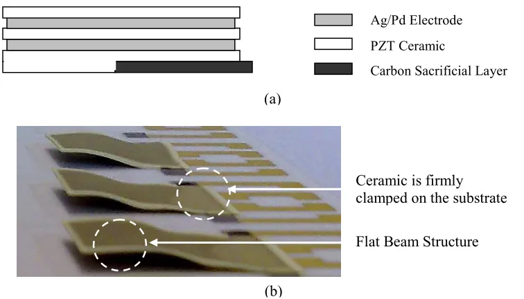
In order to prevent the development of delamination, extra layers of thick-film ceramic with similar thermal expansion coefficient where added to cover the Ag/Pd layers on both the lower and upper layer of the sandwiched structure of ceramic-electrode-PZT-electrode-ceramic as shown in Fig. 4(a). It can be seen from Fig. 4(b) that the shape of cantilevers started to be formed with its base firmly clamped on the alumina substrate. The structure that formed the flexible part is released from the substrate and revealing a free-standing form.
To address the issue of zero resultant stress at neutral axis, a multilayer arrangement of ceramic-electrode-PZT-electrode-PZT-electrode-PZT-electrode-ceramic was fabricated to increase the d -distance and hence improve the electrical charge generation when it is bent. The material for the ceramic as the cover for electrode is the similar material for constructing the active PZT piezoelectric layer to avoid crack as a result of unmatched thermal expansion when exposed to drastic change of temperature.
The resultant of co-firing is a flat cantilever structure, but it experiences of shrinkage of roughly 10% compared to their original size before co-firing as shown in Fig. 5(b). Finally the samples were then polarized at 220 V with elevated temperature of 200 °C for sample with thickness of around 50 µm, with give an electric field strength of about 4.4 MV/m.
Ag/Pd layers suffer delamination PZT Ceramic
Carbon Sacrificial Layer Ag/Pd
conductor
(a) (b)
Fig. 4 (a) Schematic (not actual scale) and (b) photograph of free-standing sandwiched cantilever structure of ceramic-Electrode-PZT-Electrode-Ceramic.
Fig. 5 (a) Schematic diagram of cantilever before co-firing and (b) photograph of thick-film free-standing structure after co-firing.
Fig. 6 (a) Multiple layer of ceramic-electrode-PZT-electrode-PZT-electrode-PZT-electrode-ceramic, with (b) direction of polarization.
(a)
h
l
Rigidly Clamped
Neutral axis of
PZT layer Centroid of
cantilever structure
d
(b)
+
-Ceramic
Ceramic Electrode PZT Electrode PZT Electrode PZT
(a) (b)
Potential Free-Standing
Structure Length,
lb
Width,
wb
Solder Pad Sacrificial
Layer
(a)
Ceramic is firmly clamped on the substrate
Flat Beam Structure
Ag/Pd Electrode
Carbon Sacrificial Layer PZT Ceramic
(b)
Inspection and Measurement Results
The composition of the paste and the fabrication process are very important in determining the formation of microstructure of the samples and hence influence the mechanical and electrical properties of the piezoelectric ceramic.
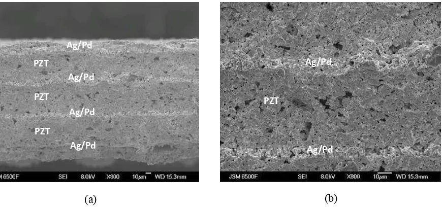
From the SEM micrographs at a magnification of 300 it can be seen clearly the layer of silver/palladium and PZT arranged in alternating pattern as shown in Fig. 7(a). Fig. 7 (b) shows the population of pores and void in the samples at a magnification of 800. The voids were formed by intercrystalline boundaries between the grains which range from several micrometers to tens of micrometers. The presence of the voids is largely due to the nature of the screen-printing process and the size of the granules used in the thick-film formulation.
Fig. 7. SEM micrographs of the thick-film piezoelectric multilayer cantilever sample, with magnification at (a) 300 and (b) 800.
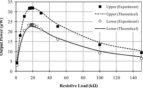
In order to investigate the performance of electrical charge generation, one of the multilayer thick-film piezoelectric cantilever samples with length of 18 mm fabricated in such a way that the thickness of lower electrode (20 µm) is greater than the upper electrode (12 µm) as shown in Fig.
7(a). The sample was clamped on an electrodynamic shaker and excited to the resonant frequency of the cantilever structure at 403 Hz with an acceleration amplitude of 0.5 g (1 g = 9.81 m/s2). The output power from each of the PZT sections was obtained by measuring the voltages across the electrode terminals sandwiched between each PZT layer when driven over a range of resistive loads from 1 kΩ to 150 kΩ.
Fig. 8 shows the output power from the upper and lower layer of the PZT cantilever. It shows that the upper section of PZT produces a higher output power at about 32 µW when driven an optimum resistive load of 18.5 kΩ compared to the lower section which produces about 24 µW.
This is because the d-distance of the upper PZT is greater than that of the lower PZT layer. The experiment results are consistent with the calculated results using equation (1), as shown in Fig. 8.
PZT
PZT PZT
Ag/Pd
Ag/Pd
Ag/Pd
Ag/Pd
PZT
Ag/Pd
Ag/Pd
(b) (a)
Fig. 8. Electrical output power measurement at upper PZT layer compared to lower PZT layer for a multilayer sample excited at its resonant frequency of 403 Hz
Conclusion
In this paper, screen-printed piezoelectric cantilever in the form of free-standing has been successfully fabricated. The flexible part of the cantilever was released from alumina substrate during co-firing process using carbon as the sacrificial layer. It was found from the fabrication outcome that an additional layer of ceramic is needed to cover the exposed electrode to prevent delamination. Without rigid substrate, the resonant frequency of the structure can be lowered to 403 Hz, however simple sandwich structure of electrode-PZT-electrode does not generate any electrical output due to zero resultant stress when the neutral axis coincide with the centroid of the cantilever structure, therefore a multilayer structure consisting of three repeating electrode-PZT-electrode was fabricated and it was found that the experimental results agree with the theoretical expectations. An electrical output power of 32 µW was recorded when the piezoelectric cantilever was excited to its
resonant at an acceleration magnitude of 0.5 g.
Acknowledgment
The authors would like to acknowledge the Malaysian Ministry of Higher Education for the research grant RAGS/2012/UTEM/TK04/1, the Faculty of Electronic and Computer Engineering, Advance Sensors and Embedded Systems (ASECs) research group, Universiti Teknikal Malaysia Melaka (UTeM) for the support of this work.
References
[1] N.M.White and J.D. Turner. Thick-film sensors: past, present and future. Meas. Sci. Technol. 8.1 (1997).
[2] N.M. White. Thick-film/ MEMS hybrid sensors. J. of Phys.: Conf. Ser. 76 (2007).
[3] Y. Wang, Y. Shi, C.Y. Zhao, J.I. Wong, X.W. Sun and H.Y. Yang. Printed all-solid flexible microsupercapacitors: towards the general route for high energy storage devices. Nanotechnology 25.9 (2014)
[4] G. Paul, R. Torah, K. Yang, S. Beeby and J. Tudor. An investigation into the durability of screen-printed conductive tracks on textiles. Meas. Sci. Technol. 25.2 (2014).
[5] Y. Kim, H. Kim and H.J. Yoo. Electrical characterization of screen-printed circuits on the fabric. IEEE Trans. Advanced Packaging, 33.1 (2010).
0 5 10 15 20 25 30 35
0 20 40 60 80 100 120 140
O
ut
pu
t P
ow
er
(µ
W
)
Resistive Load (kΩ)
Upper (Experiment) Upper (Theoretical) Lower (Experiment) Lower (Theoretical)
[6] Y. Lin, C. Andrews and H.A. Sodano. Enhanced piezoelectric properties of lead zirconate titanate sol-gel derived ceramics using single crystal PbZr0.52Ti0.48O3 cubes. J. Applied Physics, 108.6 (2010)
[7] S.H. Kim, A. Leung, C.Y. Koo, L. Kuhn, W. Jiang, D.J. Kim and A.I. Kingon. Lead-free (Na0.5K0.5)(Nb0.95Ta0.05)O3 -BiFeO3 thin films for MEMS piezoelectric vibration energy harvesting devices. Materials Letters, 69 (2012), p. 24-26.
[8] L.V. Minh, M. Hara, F. Horikiri, K. Shibata, T. Mishima and H. Kuwano. Bulk micromachined energy harvesters employing (K, Na)NbO3 thin film. J. Micromech. Microeng. 23.3 (2013).
[9] S.R. Oh, T.C. Wong, C.Y. Tan, K. Yao and F. E. Tay. Fabrication of piezoelectric polymer multilayers on flexible substrates for energy harvesting. Smart Mater. Struct. 23.1 (2014).
[10] W. Kiyotaka, T. Matsushima, H. Adachi, I. Kanno. Thin-film piezoelectric materials for a better energy harvesting MEMS. J. Microelectromechanical System. 21.2 (2012).
[11] H. Uršič, M. Hrovat, D. Belavič, J. Cilenšek, S. Drnovšek, J. Holc, M. S. Zarnik, and M. Kosec. Microstructural and electrical characterization of PZT thick films on LTCC substrates. Journal of the European Ceramic Society, 28.9 (2008), p. 1839-1844.
[12] M.F. Ab Rahman and S.L. Kok. Investigation of useful ambient vibration sources for the application of energy harvesting. IEEE Student Conference on Research and Development (SCOReD), 2011.
[13] S.L. Kok, N.M. White and N.R. Harris. Fabrication and characterization of free-standing thick-film piezoelectric cantilevers for energy harvesting. Meas. Sci. Technol. 20 (2009).
[14] S. Roundy and P.K. Wright. A piezoelectric vibration based generator for wireless electronics. Smart Materials and Structures, IOP, 23 (2004), p. 1131-1142.
[15] H. Birol, T. Maeder, C. Jacq and P. Ryser. 3-D structuration of LTCC for sensor micro-fluidic applications. European Microelectronics and Packaging Symposium, (2004).
[16] R. Torah, S.P. Beeby, and N.M. White, An improved thick-film piezoelectric material by powder blending and enhanced processing parameters. IEEE Trans.Ultrason.Ferroelectr.Freq, Control, 52.1 (2005), p. 10-16.
[17] Piezoelectric ceramics data book for designers. 1999, Morgan Electroceramics.
[18] High Quality Components and Materials for The Electronic Industry. 2003, Ferroperm Piezoceramics.
13th International Ceramics Congress - Part D
10.4028/www.scientific.net/AST.90
Screen-Printed Ceramic Based MEMS Piezoelectric Cantilever for Harvesting Energy