Faculty of Electronic and Computer Engineering
DESIGN OF SWITCHABLE MATCHED BANDSTOP FILTER
Mohd Khairy bin Zahari
MSc. in Electronic Engineering
DESIGN OF SWITCHABLE MATCHED BANDSTOP FILTER
MOHD KHAIRY BIN ZAHARI
A thesis submitted in fulfilment of the requirements for the degree of Master of Science in Electronic Engineering
Faculty of Electronic and Computer Engineering
UNIVERSITI TEKNIKAL MALAYSIA MELAKA
DECLARATION
I declare that this thesis entitle “Design of Switchable Matched Bandstop Filter” is the result of my own research except as cited in the references. The thesis has not been accepted for any degree and is not concurrently submitted in candidature of any other degree.
Signature : ………..
DEDICATION
ABSTRACT
New developments in the design of band reject filters are essential to meet the ever increasing demands on suppression of unwanted signals and miniaturization of microwave communications systems. A compact design can be achieved through the implementation of planar microstrip technology. Conventional electronically tunable bandstop filters suffer performance degradation due to the finite unloaded Q of the resonators and also the loss associated with the switching elements. Recently a new filter topology using lossy resonators has been introduced where the topology can be used to partially compensate for the loss. A frequency agile bandstop filter based on this topology has been developed, but such filters as well as conventional switchable bandstop filters encounter performance degradation in terms of tuning bandwidth and stopband bandwidth due to the frequency dependant losses and couplings. Through this thesis the filter is designed and developed an L-shape matched bandstop filter and dual mode ring resonator which can be switchable based on a lossy allpass network. The filters are integrated with switching elements that suitable for the perfectly matched bandstop concept. The lossy allpass network demonstrates the concept and design of perfectly matched bandstop response with a perfectly matched at all frequencies. The filter is based on the half-wavelength λ/2 resonator with gap coupling, parallel with an allpass nominally-90°-phase-shift element, which can be optimized to achieve high Q-factor. The switchable L-shape matched bandstop filter and switchable dual mode ring resonator can be realized by using PIN diodes as a switching elements. The dual-mode ring resonator structure is composed by two degenerate modes or splitting resonant frequencies. Two degenerate modes can be excited by perturbing stubs, notches or symmetrical feed lines. The dual-mode ring resonator stub’s is located at 135°. Both filters provide two state of operation under two conditions. The first condition is that the filter will produce allpass response when the PIN diodes are turned ‘ON’. The second condition is that the filter will produce perfectly matched bandstop response when the PIN diodes are turned ‘OFF’. The perfectly matched bandstop filter operates 1 GHz where S11 and S21 having the same attenuation at 1 GHz. For S11 must be less than 15 dB and S21 the attenuation level less than 15 dB. The allpass response having S21 ≈0.2 dB.
ABSTRAK
Perkembangan baru dalam reka bentuk padanan menolak penapis adalah penting untuk memenuhi permintaan yang semakin meningkat pada penyekatan isyarat yang tidak diingini dan pengecilan sistem komunikasi gelombang mikro. Satu reka bentuk yang padat boleh dicapai melalui pelaksanaan teknologi mikrostrip planar. Konvensional elektronik bolehubah penapis jalur henti mengalami kemerosotan prestasi akibat Q terhingga dipunggah daripada resonator dan juga kerugian yang berkaitan dengan unsur-unsur bertukar. Baru-baru ini topologi penapis baru menggunakan penyalun lossy telah diperkenalkan di mana topologi boleh digunakan untuk sebahagiannya mengimbangi kerugian. Kekerapan tangkas penapis jalurhenti berdasarkan topologi ini telah dibangunkan, tetapi penapis sedemikian serta konvensional penapis jalurhenti mudah-tukar menghadapi kemerosotan prestasi dari segi jalur lebar dan jalur lebar penalaan jalurhenti disebabkan oleh kerugian bergantung kekerapan dan gandingan. Melalui karya ini penapis direka dan dibangunkan L-bentuk dipadankan jalurhenti penapis dan dua cincin mod penyalun yang boleh mudah-tukar berdasarkan rangkaian semua-lepas lossy. Penapis yang bersepadu dengan menukar unsur-unsur yang sesuai untuk konsep sempurna dipadankan jalurhenti. Rangkaian semua-lepas lossy menunjukkan konsep dan reka bentuk tindak balas bandstop sempurna dipadankan dengan sempurna dipadankan pada semua frekuensi. Penapis adalah berdasarkan setengah gelombang λ/2 penyalun dengan gandingan jurang, selari dengan allpass ukuran-90° elemen-anjakan fasa, yang boleh dioptimumkan untuk mencapai tinggi Q-faktor. The boleh-ubah L-bentuk dipadankan jalurhenti penapis dan boleh-ubah cincin dual mod penyalun boleh dicapai dengan menggunakan diod PIN sebagai menukar unsur-unsur. Cincin dua mod struktur penyalun terdiri oleh dua merosot cara atau frekuensi salunan berpisah. Dua merosot mod boleh teruja dengan perturbing stubs, takukan atau talian makan simetri. Cincin dua mod puntung penyalun ini terletak di 135 °. Kedua-dua penapis menyediakan dua keadaan operasi di bawah dua keadaan. Keadaan pertama adalah bahawa penapis akan menghasilkan tindak balas semua lepas apabila diod PIN bertukar 'ON'. Syarat kedua ialah penapis akan menghasilkan tindak balas jalurhenti apabila diod PIN bertukar 'OFF'. Tindak balas jalurhenti akan menghasilkn jurang dibawah 15 dB dan bila dalam keadaan allpass S11 akan menghampiri 0.2 dB.
ACKNOWLEDGEMENT
Praise Allah Azza Wa Jalla and Shalawat and Salaam to Prophet Muhammad SAW, to his family, shahabah and the pious followers towards the end. In preparing this thesis, I was contact with many people. They have contributed towards my understanding and thought. I would like to express my gratitude to both my beloved parents who always support me and advise me for most of the time. Their du’a is the greatest support of all time.
In particular, I wish to express my sincere appreciation to my main thesis supervisor, Associate Professor Dr Badrul Hisham Ahmad for entrusting me with the project and for the support that he always gave during the project. Without his continued support and interest, this thesis would not have been same as presented here. I am also very thankful to my co-supervisor Dr Wong Peng Wen from Universiti Teknologi Petronas (UTP) for his guidance, advices and conduct proper research.
Special thanks to Mr Noor Azwan Shairi for helping me during my project and also to fellow postgraduate students should also be recognised for their support and provided assistance at various occasions. Their views and tips are useful indeed. Unfortunately, it is not possible to list all of them in this limited space.
LIST OF TABLES
TABLE TITLE PAGE
3.1 Design specification 25
LIST OF FIGURES
FIGURE TITLE PAGE
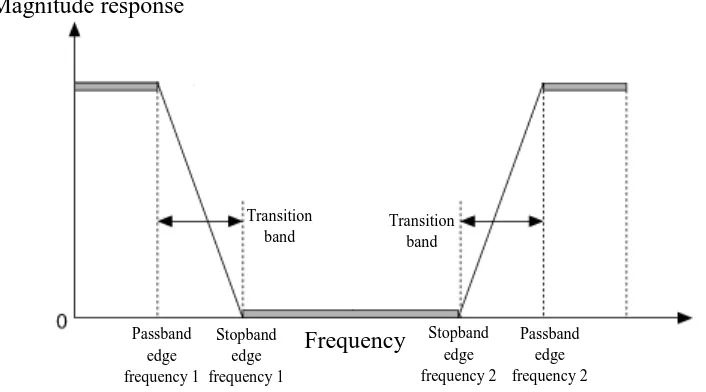
1.1 Bandstop frequency response 1
1.2 Notch bandstop frequency response 3
2.1 RF front end of a cellular base station 7
2.2 Distributed-element enhancement-Qu notch filter concept 9 2.3 Hybrid circuit implementation of a perfectly-matched notch filter 10 2.4 Even-mode admittance of a lossy resonant circuit 11
2.5 Perfectly-matched bandstop response 12
2.6 Definition of Quality Factor (Q) 13
2.7 Perturbing stub at 135° 14
2.8 Balance and unbalance ring response with perturbed stub at Φ = 45°
15
2.9 Layer of a PIN diode 17
2.10 Series SPST switch 18
2.11 Shunt SPST switch 19
3.1 Flow Chart 21
3.2 Generalized coupled-resonator model of a matched notch filter 24 3.3 Coupled resonator design with the desired parameter for the
matching bandstop filter
24
3.4 Line Calculation Tool 26
3.5 UV exposure 27
3.6 Etching process 27
3.7 Measurement and tuning process 28
3.8 Schematic design of matched bandstop filter with parameter 29 3.9 Design of switchable matched bandstop filter using biasing line 30 3.10 Design of switchable matched bandstop filter using RF
choke/inductor
31
3.11 Schematic of dual mode ring resonator matched bandstop filter 32 3.12 Design of switchable dual mode ring resonator matched bandstop
filter with biasing line
33
3.13 Layout of dual mode ring resonator matched bandstop filter using and inductor
34
3.14 Schematic testing of matched bandstop filter with PIN diode 35 3.15 Matched bandstop response when PIN diode in OFF state 36 3.16 Allpass response when PIN diode in ON state 36 3.17 Schematic testing of switchable dual mode ring resonator
matched bandstop filter with PIN diode
37
3.18 Matched bandstop response when the PIN diode in reverse biased.
37
3.19 Allpass response when PIN diode in forward biased 38
4.1 Layout of matched bandstop filter 40
4.2 Matched bandstop responses 40
4.3 Layout of switchable matched bandstop filter using biasing line. 41 4.4 Layout of switchable matched bandstop filter using RF 42
choke/inductor
4.5 Layout of dual mode ring resonator matched bandstop filter 43 4.6 Simulation and momentum of dual mode ring resonator matched
bandstop filter
43
4.7 Layout of switchable dual mode ring resonator matched bandstop filter with biasing line
44
4.8 Layout of dual mode ring resonator matched bandstop filter using an RF choke / inductor
44
4.9 Switchable matched bandstop filter 45
4.10 Matched bandstop response when PIN diode turned OFF 46
4.11 Allpass response when PIN diode turned ON 46
4.12 Switchable matched bandstop filter using an RF choke / inductor 47 4.13 Matched bandstop response when PIN diode turned OFF 47
4.14 Allpass response when PIN diode turned ON 48
4.15 Comparison of Matched bandstop response using biasing line and RF choke/Inductor
49
4.16 Prototype of switchable dual mode ring resonator matched bandstop filter using biasing line
49
4.17 Matched bandstop response when PIN diode turn OFF 50
4.18 Allpass response when PIN diode turn ON 51
4.19 Prototype of Switchable dual mode ring resonator matched bandstop filter
51
4.20 Fabrication result of dual mode ring resonator matched bandstop filter when reverse biased (PIN diode OFF state)
52
4.21 Fabrication result of dual mode ring resonator matched bandstop filter when forward biased (PIN diode ON state)
53
4.22 Shows the comparison between using biasing line and RF choke/ inductor
53
4.23 The analysis of distance of coupled line has been investigated and shows the different value of coupling gap versus the band stop at 1 GHz
54
4.24 Fabrication result of dual mode ring resonator matched bandstop filter when forward biased (PIN diode ON state)
55
LIST OF SYMBOLS
λg - Guide wavelength
λ0 - Center frequency wavelength
λg0 - Center guide
�0 - Center frequency of interest
�� - Cut off frequency
K - Characteristic impedance of impedance inverter
εr - Dielectric constant
α - Attenuation constant
µ - dielectric permeability
β - Propagation constant
C - Capacitor
L - Inductor
Z - Impedance
[T] - Transfer matrix
Rs - Series resistance under forward bias
CT - total capacitance at zero or reverse bias
RD - parallel resistance at zero or reverse bias
VR - maximum allowable DC reverse bias voltage
τ - carrier lifetime
ϴAVE - average thermal resistance or
PD - maximum average power dissipation
ϴpulse - pulse thermal impedance or
PP - maximum peak power dissipation
LIST OF PUBLICATIONS
The research papers produced and published during the course of this research are as follows:
1. Zahari, M.K.; Ahmad, B.H.; Shairi, N.A.; Peng Wen Wong 2011. Reconfigurable matched bandstop filter. RF and Microwave Conference (RFM), IEEE International , vol., no., pp.230-233, Seremban, Malaysia, 12-14 Dec. 2011
2. Zahari, M.K.; Ahmad, B.H.; Shairi, N.A.; Peng Wen Wong 2012. Reconfigurable dual mode ring resonator matched bandstop filter. IEEE Symposium on Wireless Technology & Application (ISWTA 2012), Bandung, Indonesia, 23-26 Sept. 2012
3. Zahari, M.K.; Ahmad, B.H.; Shairi, N.A.; Peng Wen Wong, 2012. Design and Comparison of Reconfigurable Perfectly-Matched Bandstop Filter. In: International Journal of Electronics and Computer Science and Engineering
(IJECSE). (Submitted)
TABLE OF CONTENT
PAGE
ABSTRACT i
ABSTRAK ii
ACKNOWLEDGEMENT iii
LIST OF TABLES iv
LIST OF FIGURES v
LIST OF SYMBOLS x
LIST OF PUBLICATIONS xii
Chapter 1 INTRODUCTION 1.1Project overview 1.2Problem statements 1.3Objectives
1.4Scopes of project 1.5Contribution of Project 1.6Thesis structure
Chapter 2 LITERATURE REVIEW 2.1Introduction
2.2Enhanced Qu Passive Notch Filters
2.3Perfectly-matched concept (lossy allpass network) 2.4 Selectivity
2.5 Dual mode resonator bandstop filter
2.5.1 Dual mode ring resonator bandstop filter 2.6Review of Switchable Filter
2.7PIN diode
2.7.1 Fundamental
2.7.2 PIN Diode Application 2.8Summary Chapter 3 METHODOLOGY
3.1Introduction 3.2Flowchart
3.2.1 Literature review
3.2.2 Design and simulation of matched bandstop filter 3.2.3 Optimization and fabrication
3.2.4 Measurement and analysis 3.3The design of resonator
3.4Matched bandstop filter design 3.4.1 Perfect notch concept 3.4.2 Design specification 3.5Simulation
3.6Hardware design
3.6.1 Generate mask on transparency 3.6.2 Photo exposure process
3.7Filter design
3.8Design of matched bandstop filter 3.9Switchable matched bandstop filter
3.9.1 Switchable filter using biasing line
3.9.2 Switchable filter using RF choke/inductor
3.10Design of dual mode ring resonator matched bandstop filter
3.10.1 Switchable Dual Mode Ring Resonator Matched Bandstop Filter using Biasing Line
3.10.2 Switchable Dual Mode Ring Resonator Matched Bandstop Filter using an RF choke / inductor
3.11 Analysis of filter circuits simulation using PIN diode 3.12 Summary Chapter 4 RESULT AND DISCUSSION
4.1Design specification 4.2Simulation result
4.2.1 Design of matched bandstop filter 4.2.2 Switchable matched bandstop filter
4.2.2.1Switchable using biasing line
4.2.2.2Switchable using RF choke/inductor
4.2.3 Design of dual mode ring resonator matched bandstop filter 4.2.3.1Switchable using biasing line
4.2.3.2Switchable using RF choke/inductor 4.3Fabrication result
4.3.1 Switchable matched bandstop filter (biasing line)
4.3.2 Switchable matched bandstop filter (RF choke/inductor) 4.3.3 Comparison of Switchable matched bandstop filter using
biasing line and RF choke/inductor
4.3.4 Switchable dual mode ring resonator matched bandstop filter using biasing line
4.3.5 Switchable dual mode ring resonator matched bandstop filter using RF choke/inductor
4.3.6 Comparison of simulation and fabrication for reconfigurable dual mode ring resonator matched bandstop filter
4.4 Summary
46 48
50
51
54
55 Chapter 5 CONCLUSION AND RECOMMENDATIONS FOR FUTURE
WORK 5.1Conclusion 5.2Future work
56 57
REFERENCES 58
CHAPTER 1
INTRODUCTION
1.1 Project Overview
The increasing development of microwave and millimeter-wave communication system has promoted the need for suppression of multiple unwanted signals for military broadband applications (Han et. al., 2006). Thus, high performance and miniaturize size of bandstop filter is investigated. Bandstop and bandpass filters (Ni et. al., 2006) (Jin et. al., 2006) (Zhang et. al. , 2007) play an important role in microwave and millimeter-wave system, which are applied to discriminate the desired and unwanted signals.
Bandstop filter provides an overhaul of communication system that contains unwanted signal or interferences (Saxena et. al., 2008). Bandstop filter was applied in an active element circuit design such as a mixer and oscillator to remove higher order harmonics and other spurious signal (Hsieh et. al., 2005). For an ideal Bandstop filter, an attenuation of frequencies will occur at above its lower cut-off frequencies and below its upper cut-off frequencies. On the other hand, for frequencies greater than the upper cutoff and frequencies less than the lower cutoff the signal is allowed to pass which known as pass-band region. Figure 1.1 shows the basic frequency response of a bandstop filter.
Band-stop filters are key components in a microwave communication front-end to isolate frequency band located within a wide pass-band. In active circuit design such as oscillators and mixers, bandstop filters were applied to remove higher order harmonics and other spurious signal. When the stop-band is narrow, it is called a band notch filter. In the past, most conventional resistor/inductor/capacitor (RLC) bandstop filters has included several types of open-circuited stubs or shunt stubs of a quarter wavelengths that suffer from a number of technical limitations which are associated with the use of inductors. In a microwave filter, the energy is differentially reflected in order to realize frequency selectivity which is limited by the lossless associated with the technology used. Passive method approached that implement a narrowband bandstop filter with theoretically infinite stopband attenuation while being perfectly matched in both the passband and stopband. Highly-selective filters are a necessity for many applications such as communications transceivers and radar systems. As filter selectivity is limited by the losses associated with the technology used to realize the filter, it is desirable to use design techniques which take the effects of losses into account. The work utilizes a passive approach to implement a narrowband bandstop filter with theoretically infinite stopband attenuation, while being perfectly matched in both the passband and stopband (Hamzah, 2010).
The implementation of a notch concept of the filter is to produce a maximum attenuation for bandstop filter. This is used to remove a narrow band of frequencies from the signal path (Jachowski, 2004).
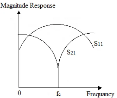
At present, demand for high performance and switchable bandstop filter is a necessity in many communication applications. The switchable filters can reduce the complexity of a system by allowing filter switchable instead of having switched filter banks. Moreover, implementation of a notch concept of the filter producing a maximum attenuation for bandstop filters as shown in Figure 1.2. This is used to remove a narrow band of frequencies from the signal path (Jachowski, 2004).
Figure 1.2 Notch bandstop frequency responses
However, losses in the system material or the appearance of an active device such as diode (Hunter et. al., 1998) affect the quality factor of the filter. Normally response of the input reflection (S11) and forward transmission coefficient (S21) in the conventional bandstop filter is shown in Figure 1.2. The S11 is the input reflection where the input energy is reflected back to an input port. Thus, this condition is bad because the reflected energy could damage the input device. It is better to have a response that will forward the entire signal to the output. That's known as a matched bandstop filter.
For that reason, the switchable matched bandstop filter has been proposed with the implementation of perfectly-matched bandstop filter to overcome this drawback. (Guyette et. Al., 2005) proved that the network is perfectly-matched and give a bandstop response with maximum attenuation at center frequencies even by applying lossy resonator circuit. This project is based upon the topology of perfectly-matched bandstop filter and K-inverter topology for lossy resonator which consist the parallel coupled of λ/2 a short circuit transmission line that produced a nominally-90°-phase shift element between the resonator couplings in one structured. This design approaches a perfectly match at all frequencies and to show that the perfectly-matched bandstop filter topology allows switchable by adding a switching element which is consist of the PIN diode, chip capacitor biasing line and resistor. The performance of filter frequency response is analysed in several aspects such as rejection, return loss, insertion loss and the 3 dB quality factors, Q (Guyette et. al., 2005).
1.2 Problem Statements
New Development in the design of band rejects filter and Highly-selective filters are a necessity for many applications. This design is to meet the ever increasing demands on suppression of unwanted signals and miniaturization of microwave communications systems. As filter selectivity is limited by the losses associated with the technology used to realize the filter, it is desirable to use design techniques which take the effects of losses into account. Active approaches suffer from issues such as their inherent nonlinearity which makes their use for many applications limited (Hunter, 2005).
Conventional electronically tunable bandstop filters suffer performance degradation due to the finite unloaded Q of the resonators and also the loss associated with the tuning elements (Hunter, 2005). Recently a new filter topology using lossy resonators has been introduced where the topology can be used to partially compensate for the loss (Hunter et. al., 2005). A frequency agile bandstop filter based on this topology was presented (Jachowski, 2005), but such filters as well as conventional tunable bandstop filters encounter performance degradation in terms of tuning bandwidth and stopband bandwidth due to the frequency dependant losses and coupling. Such an impedance inverter is made tunable to provide the optimum inter-resonator coupling using a varactor diode.
The tunability of the inverter properties can be used to compensate for the frequency dependant couplings in the conventional tunable bandstop filters to retain the optimum stopband bandwidth or loaded Q while tuning the center frequencies, thus maximizing the available tuning bandwidth. Reconfigurable filter with relative bandwidth tuning was presented (Rauscher, 2003) (Sanchez et. al., 2005), where the bandwidth tuning is accomplished by changing the coupling among filter resonators. The filters were realized with some additional transmission line segments with the attached varactor diodes or switch elements, in order to achieve the inter-resonator coupling tuning.
Therefore, switchable filters can reduce the complexity of a system by allowing filter re-configurability instead of having switched filter banks. As a result, Switchable Matched Bandstop Filter is proposed to offer selectivity (all pass band or bandstop) filtering.
1.3 Objectives
The objectives of this project are stated as below:
1. To design and develop a matched bandstop filter with L-shape and dual mode ring resonator that are switchable.
2. To integrate between the filter and switching elements that suitable for the perfectly-matched bandstop concept.
1.4 Scopes of Project
This project focuses on three main areas. First, understand the filter concept by data acquisition of literature review on bandstop filter, the concept of perfectly-matched bandstop and integration of switching element into matched bandstop topology. The filters are designed into four prototypes which are matched bandstop filter with L-shape resonator and dual mode ring resonator. Lastly, the filters are integrated with biasing line and RF choke and also the PIN diode as the switch elements. The perfectly matched bandstop will be integrated with switches onto the resonator such that the response is switchable. Therefore, switchable filters can reduce the complexity of a system by allowing filter switchable instead of having switched filter banks. As a result, Switchable Matched Bandstop Filter is proposed to offer selectivity (all pass band or bandstop) filtering.
1.5 Contribution of research
The contributions in this research mainly focus on switching element that integrate
with matched bandstop topology either to switch from bandstop response to Allpass or vice versa. This design is proposed based on the implementation of perfectly-matched bandstop filter for L-shape resonator and dual mode ring resonator. This project can be applied for RF front end transceiver system.
1.6 Thesis Structure
This thesis is divided into five chapters. The five chapters consist of introduction, literature review, methodology, result and discussion.
The first chapter are an introduction about microwave filter, objectives, problem statements, and scope of the project and also the structure of the thesis.