Paper:
Fabrication of Microstructures on RB-SiC by Ultrasonic
Cavitation Assisted Micro-Electrical Discharge Machining
Pay Jun Liew
∗,∗∗∗, Keita Shimada
∗, Masayoshi Mizutani
∗,
Jiwang Yan
∗∗, and Tsunemoto Kuriyagawa
∗∗Department of Mechanical Systems and Design, Tohoku University
6-6-01 Aoba, Aramaki, Aoba-ku, Sendai 980-8579, Japan E-mail: [email protected]
∗∗Department of Mechanical Engineering, Faculty of Science and Technology, Keio University
3-14-1 Hiyoshi, Kohoku-ku, Yokohama 223-8522, Japan
∗∗∗Manufacturing Process Department, Faculty of Manufacturing Engineering, Universiti Teknikal Malaysia Melaka
Hang Tuah Jaya, 76100 Durian Tunggal, Melaka, Malaysia [Received March 31, 2013; accepted August 5, 2013]
Ultrasonic cavitation assisted micro-electrical dis-charge machining was used to fabricate microstruc-tures on reaction-bonded silicon carbide. To aid the removal of debris from the machining gap and to ob-tain a good surface finish, carbon nanofibers were added into the dielectric fluid. The suspension of car-bon nanofibers in the dielectric fluid and the cavitation bubble effect induced by the vibration of the dielectric fluid proved to be effective in reducing the deposition of tool material on the workpiece surface. The tool ma-terial deposition rate was found to be significantly af-fected by the vibration amplitude and the distance be-tween the oscillator and the workpiece. With a hemi-spherical electrode and inclined workpiece, high accu-racy micro-dimples could be obtained within a short time. A nanometer-level surface finish was success-fully obtained on a hard-brittle RB-SiC mold material.
Keywords: micro-dimple array, ultrasonic cavitation, micro-electro discharge machining, carbon nanofiber, reaction-bonded silicon carbide
1. Introduction
In recent years, the industrial demand for microstruc-tures such as micro-dimple arrays, micro-pyramid arrays and micro-prism arrays has been increasing. Because of the wide range of applications of these functional crostructures in optical, biomedical engineering, and mi-croelectromechanical systems, precision manufacturing processes have become essential to produce these mi-crostructured surfaces, not only in terms of their dimen-sions and shape, but also in terms of the quality of the machined surface [1].
There are many different fabrication methods for pro-ducing microstructures, such as photolithography [2],
laser machining [3], dry etching [4], and a hybrid pro-cess that includes ultraviolet lithography, photoresist re-flow processing, electroplating and a hot embossing tech-nique [5]. Micro mechanical machining processes also have been used to fabricate micro-functional surface on metal and ceramic surfaces. A typical example is the use of tungsten carbide micro-endmills as micro-cutting tools [6–7]. However, commercial micro-endmills with small diameters are easily fractured, and it is difficult to detect tool wear and fracture [6]. As an alternative ap-proach, Zhang et al. [8] used a polycrystalline diamond micro-endmill to fabricate micro-dimple arrays on a tung-sten carbide workpiece.
Recently, micro-electro discharge machining has re-ceived attention from researchers as a precision machin-ing tool for producmachin-ing micro-features, such as in the fab-rication of micro-molds for plastic and glass lenses. The growing popularity of micro-electrical discharge machin-ing can be attributed to its advantages, which include low installation cost and its ability to machine complex three-dimensional shapes easily regardless of the mate-rial’s hardness [9]. Furthermore, during machining with micro- electrical discharge machining, there is no direct contact between the electrode and the workpiece, which eliminates mechanical stress, chatter, and vibration prob-lems [10].
hy-trode tip concavity. Furthermore, with the addition of carbon nanofibers, the tungsten tool material deposition can also be reduced compared to that obtained using only pure EDM oil [11, 16]. Therefore, in the present work, we attempted to use this hybrid process, to suppress the tool material deposition during the fine finishing of mi-crostructures by using EDM. The effect of tool shape and time controlling strategies for this fine finishing were ex-perimentally investigated.
2. Experimental Methods
2.1. Equipment and Materials
The experiments were conducted on a standard micro-electrical discharge machining machine (Panasonic MG-ED82W). This machine has a Resistor-Capacitor (RC) discharge circuit, and enables both micro wire EDM and micro die sinking machining. The discharging energy can be changed by adjusting the voltage (0 – 110 V), and/or the electrical capacitance of the RC circuit. The electrical capacitance is determined by condensers C1 – C4, which possess capacitance of 3300, 220, 100 and 10 pF, respec-tively. The stray capacitance of the circuit (C0) is approx-imately 1 pF. An ultrasonic vibration device, the SC–450 cavitation generator (Taga Electric Co., Ltd, Japan) with a power output of 50 W was used in this experiment. It has a vibration frequency of 20 kHz and a maximum amplitude of 14 µm. During the EDM process, the tool electrode was inserted through a small hole into the end of the os-cillator horn of the cavitation generator. Ultrasonic vibra-tion was applied to the dielectric fluids by the oscillator horn, which caused the cavitation effect. The workpiece material used in the experiments was RB-SiC, an impor-tant ceramic material that has a high electrical resistivity (∼1453Ωcm). RB-SiC is a promising material for fab-ricating the molding dies used in a glass molding press. The as-received sample was produced by Japan Fine Ce-ramics Co., Ltd. Some of the typical material properties of the sample are listed inTable 1. Tungsten was used as tool electrode because of its high melting point and low tool wear. Commercially available EDM oil, Casty Lube EDS (Nikko Casty Co., Ltd.), was used as the dielectric fluid. To improve the discharge frequency, 0.06 g/L of high conductivity carbon nanofibers measuring 150 nm in diameter and 6 – 8µm in length were used as additives.
Table 2. Experimental conditions for fabrication of micro tool electrodes.
2.2. Fabrication of Micro-Tool Electrode
Fig. 1. Experimental setup using inclined workpiece.
was selected as the tool material because of its high con-ductivity and high wear resistance. This method was sim-ilar to that described by Ravi and Han [18] and Perveen et al. [19]. For WEDG, a brass wire electrode was contin-uously fed on the guide, and the tungsten workpiece was moved perpendicularly to the wire in theZandX direc-tions, at a rotational speed of 3000 rpm.
2.3. Micro-Dimple Machining
First, the tungsten tools shaped by the procedure ex-plained in the preceding section were used to machine micro-dimples on RB-SiC. Using die sinking EDM, each test was run for a 5 min, during which a negative electrode polarity was used. The effect of the machining time on the fine finishing was experimentally investigated. During the machining, the dielectric fluid was ejected through a noz-zle to the machining area (external side flushing) to en-hance the flushing of debris. The workpiece was set at a 10◦angle, as schematically shown in Fig. 1. It was ex-pected that the slight incline of the workpiece would con-tribute to the smooth exclusion of tungsten debris, and in turn, result in a better surface finish.
Thereafter, a combination of ultrasonic cavitation and carbon nanofibers [15] was used to control the tool mate-rial deposition on the RB-SiC machined surface. Fig. 2
shows a schematic diagram of the experimental setup. The vibration amplitudes and distance between the oscil-lator and the workpiece were changed, and the extent of material migrations from the tool electrode to the RB-SiC workpiece was investigated experimentally. Each micro-electrical discharge machining test was performed on a sample for a duration of 3 min.
All of the experiments were repeated three times with newly fabricated tool electrodes, which rotated at a ro-tational speed of 3000 rpm during the machining of the dimples. Subsequently, the optimal conditions to improve the form accuracy and finished surface topography were used to fabricate a micro-dimple array. The experimental conditions are summarized inTable 3.
Fig. 2. Schematic diagram of ultrasonic cavitation assisted micro-electrical discharge machining experimental setup.
Table 3. Experimental conditions.
2.4. Surface Characterization
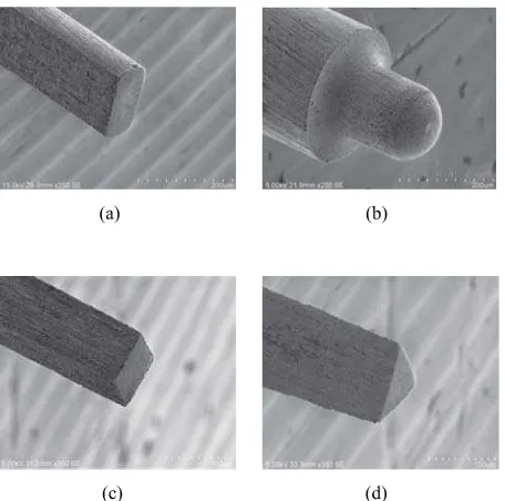
Fig. 3. Microelectrodes with different geometries: (a) rect-angular, (b) hemispherical, (c) square, and (d) triangular.
3. Results and Discussion
3.1. Effect of Tool Shape
Figure 3shows SEM micrographs of the tungsten tool electrodes with different geometries, which were fabri-cated by using the procedures described in section 2.2. Electrodes of exactly the same size should be used in such experiments to allow a comparison of machining results. However, it is difficult to do this in practice. Therefore, electrodes with diameters between φ90 and φ150 µm were used in this study.
Without ultrasonic cavitation, micro-dimples were ma-chined on the RB-SiC workpiece using the fabricated mi-croelectrodes. The fine finishing parameters were set to 80 V and stray capacitance (∼1 pF). The machining was performed for a constant machining time of 5 min.Fig. 4
shows the SEM micrographs of the machined micro-dimples that were obtained with an inclined workpiece. It is clear that none of the dimples show good form accuracy, and that a cone-shaped protrusion was formed at the cen-ter of each micro-dimple. In addition, the micro-dimples that were fabricated by the rectangular, square, and trian-gular electrodes show concentric rings inside the dimples. This is assumed to be because of nonuniform wear of the flat-head electrode tip, which might have been caused by long machining time. During fine finishing at a low volt-age, the gap between the tool and the workpiece is very small. Therefore, the electrical discharge-induced tung-sten debris cannot be effectively removed from the gap by using a flat-head electrode; instead, the debris is de-posited on the machined surface and/or interacts with the tool electrode [20], causing nonuniform wear of the tool tip. In contrast, the hemispherical electrode, which was
Fig. 4. Micro-dimple machined at 80 V, stray capacitance using different geometry micro tool electrodes: (a) rectan-gular, (b) hemispherical, (c) square, and (d) triangular.
non-flat head electrode, could produce better form accu-racy without concentric rings inside the micro-dimple.
Thus, the next section describes step-by-step machin-ing (from rough to fine finishmachin-ing) that was conducted to control the form accuracy of the micro-dimples by using a hemispherical electrode.
3.2. Effect of Machining Time on Fine Finishing To obtain micro-dimples with high form accuracy, step-by-step machining (from rough to fine finishing) was car-ried out using an inclined workpiece. Roughing regimes use a high pulse energy to remove the bulk of the material in the minimum amount of time. Semifinishing and finish-ing regimes use low-energy relaxation pulses to achieve a good surface finish and accurate geometry [21]. First, the micro-dimple shape was formed by a hemispherical electrode using roughing parameters (voltage 100 V, ca-pacitance 3300 pF). It was then finished under finishing conditions (voltage 80 V, stray capacitance∼1 pF).
Fig. 5. Micro-dimples finished with different machining times: (a) 10 s, (b) 50 s, and (c) 70 s.
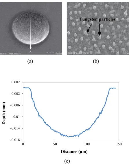
Fig. 6. SEM micrograph of micro-dimple: (a) general view, (b) detailed view of dimple surface, and (c) cross-sectional profile of machined micro-dimple along direction A in (a).
By using the aforementioned method, a micro-dimple was machined on RB-SiC, as shown inFig. 6(a).Fig. 6(c)
shows a cross-sectional profile of the dimple, which was measured along direction A inFig. 6(a). It can be seen that a good form accuracy without a cone-shaped
protru-Fig. 7. Surface roughness profile of micro-dimple inFig. 6(a).
sion could be obtained with an inclined workpiece. How-ever, as explained in [11], tungsten electrode material was found to be deposited on the machined surface, as micro-particles in an amorphous structure inside surface craters, and as a thin interdiffusion layer with a poly-crystalline structure on flat surface regions, as shown inFig. 6(b). As a result, the surface roughness increased, which deterio-rated the surface integrity of the micro-dimple. To further confirm the surface roughness of the machined surface, measurement was performed using a laser-probe profiling system. The evaluation length was 50µm, across the cen-ter of the micro-dimple along the radial direction. Fig. 7
shows a surface profile corresponding to the micro-dimple shown inFig. 6(a). This observation was in good agree-ment with the microstructure observation, where the fin-ished surface was quite rough, with a surface roughness of 0.1410µmRa. This indicates that without ultrasonic cav-itation, the step-by-step machining with an optimized fin-ishing time on an inclined surface is helpful in obtaining good form accuracy; however, it cannot prevent electrode material deposition on the machined surface.
3.3. Effect of Vibration Amplitude
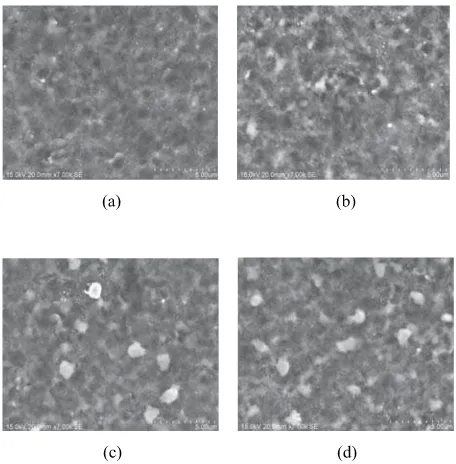
Next, to suppress the deposition of tungsten particles, ultrasonic cavitation assisted micro-electrical discharge machining with the addition of carbon nanofibers in the dielectric fluid, as explained in the previous work [15], was conducted on RB-SiC. Fig. 8 shows SEM micro-graphs of machined RB-SiC surfaces obtained using dif-ferent vibration amplitudes, ranging from 0 to 100%. When ultrasonic cavitation was not used, the quantity of the deposited tungsten particles was high, as shown in
Fig. 8(a). However, as the amplitude increased (100%, ∼14µm), there was a rapid decrease in the amount of deposited tungsten particles, as shown in Fig. 8(d). To further confirm the deposited tungsten elemental compo-sition, the machined surface was analyzed using EDX.
Fig. 8. Machined surface at 80 V and stray C, but with different levels of vibration amplitude and carbon nanofiber addition: (a) without ultrasonic cavitation, (b) 20%, (c) 60%, and (d) 100%.
Fig. 9. Effect of vibration amplitude on weight percentage of deposited tungsten electrode material.
According to Vyas and Preece [22], at an extremely low vibration amplitude, the acoustic intensity is insuf-ficient to produce cavitation, which makes it difficult to remove the debris from the working area. As the ampli-tude of the vibration increases, even though the number of bubbles increases, the formation of cloud cavitation is still marginal and insufficient to flush out the debris to a sig-nificant degree. Consequently, unremoved debris remains on the machined surface, as shown inFigs. 8(b)and(c). At a critical amplitude (in this case, 14µm), the number of bubbles increases significantly [22], and as a result of the pressure fluctuation that is induced by the ultrasonic waves, the generated cloud cavitation tends to oscillate rapidly at the working area, as explained in [15]. There-fore, the electrical discharge-induced tungsten debris can be effectively removed from the narrow gap through cloud
Fig. 10. Machined surfaces at 80 V and stray C but with different working distances: (a) 1 mm, (b) 2 mm, (c) 3 mm, and (d) 4 mm.
cavitation, resulting in a better surface finish with min-imum deposition of tungsten particles. On the basis of these results, we can say that it is important to increase the vibration amplitude to suppress the tungsten material deposition. In this study, the optimal value of vibration amplitude was 100%, which was around 14µm.
3.4. Effect of Working Distance
The effect of the working distance on the deposition of tungsten tool material on the machined surface was in-vestigated. The results are shown inFig. 10. The work-ing distance in this context means the distance between the oscillator and the workpiece during the EDM process. The working distance ranged from 1 to 4 mm at a constant amplitude of 14 µm (100%). It is seen that the quantity of the deposited particles increases when a longer work-ing distance is used, as shown inFig. 10(d). In contrast, a short working distance contributed to a significant re-duction in the deposited tungsten particles (Fig. 10(a)). Presumably, when the working distance was longer, the cloud cavitation was not strong enough to reach the work-ing area. Hence, the tungsten debris could not be removed significantly, and instead, deposited on the machined sur-face.
3.5. Fabrication of Micro-Dimple Array
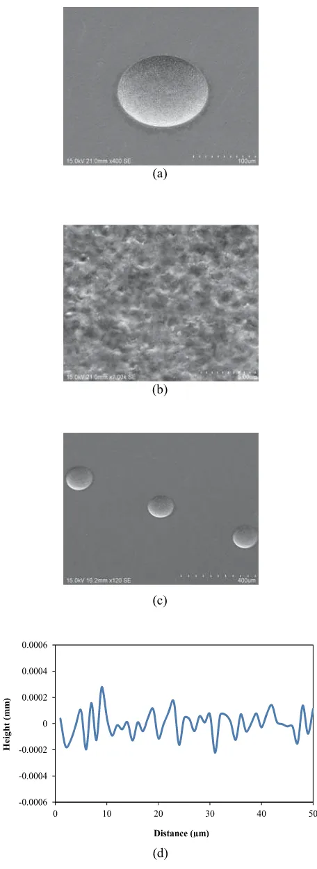
Using the optimum machining conditions obtained in the previous sections, a micro-dimple array was fabri-cated on the RB-SiC mold material. Fig. 11(a)shows an SEM micrograph of a single dimple. Good form accu-racy without a cone-shaped protrusion was obtained us-ing the fine finishus-ing conditions of 80 V and stray capac-itance. Fig. 11(b)shows a magnified view of the dimple surface. Clearly, the adherence of tungsten particles could be significantly suppressed by the combination of ultra-sonic cavitation and carbon nanofibers, where the amount of deposited tungsten micro particles was minimal. The surface roughness was measured across the center of the micro-dimple, and the evaluation length was 50µm. The surface profile is shown inFig. 11(d). It should be noted that the surface roughness of the micro-dimple improved significantly, and a nanometer-level surface roughness (78.1 nmRa) could be obtained. The finished surface was far smoother than that inFig. 6.Fig. 11(c)shows an SEM micrograph of a fabricated micro-dimple array. This re-sult demonstrated that the ultrasonic cavitation assisted micro-electrical discharge machining with the addition of carbon nanofibers in the dielectric fluid and a slightly in-clined workpiece were helpful for obtaining high form ac-curacy and a good surface finish on the RB-SiC machined surface, provided a suitable machining time was used for the fine finishing.
4. Conclusion
Ultrasonic cavitation assisted micro-electrical dis-charge machining experiments were performed with the addition of carbon nanofibers in the dielectric fluid. The effects of the vibration amplitude, working distance, elec-trode shape and machining time were investigated. The following conclusions were drawn:
1. Ultrasonic cavitation assisted micro-electrical dis-charge machining with carbon nanofibers added to the dielectric fluid can significantly reduce the de-position of tool material on the workpiece surface, which in turn, improves the surface finish of the ma-chined surface.
2. The vibration amplitude is closely related to the de-position of the tool material, with a higher amplitude resulting in a lower deposition rate.
3. Decreasing the distance between the oscillator and the workpiece is helpful in preventing the deposition of the tool material.
4. Neglecting the cone-shaped protrusions, hemispher-ical tools produce better form accuracy without con-centric rings inside the micro-dimple as compared to other microelectrode shapes.
5. With an inclined workpiece and suitable fine-finishing time (∼70 s), high form accuracy could be obtained for a micro-dimple.
Fig. 11. SEM micrographs of machined micro-dimples:
Melaka (UTeM) for her Ph.D. scholarship.
References:
[1] J. C. Hung, J. K. Lin, B. H. Yan, H. S. Liu, and P. H. Ho, “Us-ing a helical micro-tool in micro-EDM combined with ultrasonic vibration for micro-hole machining,” J. of Micromechanics and Mi-croengineering, Vol.16, pp. 2705-2713, 2006.
[2] M. H. Wu and G. M. Whitesides, “Fabrication of two-dimensional arrays of microlenses and their applications in photolithography,” J. of Micromechanics and Microengineering, Vol.12, pp. 747-758, 2002.
[3] C. C. Chiu and Y. C. Lee, “Fabricating of aspheric micro-lens array by excimer laser micromachining,” Optics and Lasers in Engineer-ing, Vol.49, pp. 1232-1237, 2011.
[4] M. B. Stern and T. R. Jay, “Dry etching for coherent refractive mi-crolens arrays,” Optical Engineering, Vol.33, No.11, pp. 3547-3551, 1994.
[5] C. T. Pan and C. H. Su, “Fabrication of gapless triangular micro-lens array,” Sensors and Actuators A, Vol.134, pp. 631-640, 2007. [6] I. S. Kang, J. S. Kim, M. C. Kang, and K. Y. Lee, “Tool condition
and machined surface monitoring for micro-lens array fabrication in mechanical machining,” J. of Materials Processing Technology, Vol.201, pp. 585-589, 2008.
[7] H. Weule, V. Huntrup, and H. Tritschler, “Micro-cutting of steel to meet new requirements in miniaturization,” CIRP Annals-Manufacturing Technology, Vol.50, pp. 61-64, 2001.
[8] Z. Zhang, H. Peng, and J. Yan, “Micro-cutting characteristics of EDM fabricated high-precision polycrystalline diamond tools,” Int. J. of Machine Tools and Manufacture, Vol.65, pp. 99-106, 2013. [9] D. Reynaerts, W. Meeusen, and H. V. Brussel, “Machining of
three-dimensional microstructures in silicon by electro-discharge machin-ing,” Sensors and Actuators A, Vol.67, pp. 159-165, 1998. [10] K. H. Ho and S. T. Newman, “State of the art electrical
dis-charge machining (EDM),” Int J. of Machine Tools and Manufac-ture, Vol.43, pp. 1287-1300, 2003.
[11] P. J. Liew, J. Yan, and T. Kuriyagawa, “Experimental investiga-tion on material migrainvestiga-tion phenomena in micro-EDM of reacinvestiga-tion- reaction-bonded silicon carbide,” Applied Surface Science, Vol.276, pp. 731-743, 2013.
[12] R. Garn, A. Schubert, and H. Zeidler, “Analysis of the effect of vibrations on the micro-EDM process at the workpiece surface,” Precision Engineering, Vol.35, pp. 364-368, 2011.
[13] K. T. Hoang and S. H. Yang, “A study on the effect of different vibration-assisted methods in micro-WEDM,” J. of Materials Pro-cessing Technology, Vol.213, pp. 1616-1622, 2013.
[14] T. Ichikawa and W. Natsu, “Realization of micro-EDM under ultra-small discharge energy by applying ultrasonic vibration to machin-ing fluid,” Procedia CIRP, Vol.6, pp. 326-331, 2013.
[15] P. J. Liew, J. Yan, and T. Kuriyagawa, “Fabrication of micro deep holes on reaction-bonded SiC by ultrasonic cavitation assisted mi-cro EDM,” Int. J. of Machine Tools and Manufacture. (In press) [16] P. J. Liew, J. Yan, and T. Kuriyagawa, “Carbon nanofiber assisted
micro electro discharge machining of reaction-bonded silicon car-bide,” J. of Materials Processing Technology, Vol.213, Issue 7, pp. 1076-1087, 2013.
[17] Technical data provided by the manufacture of the workpiece mate-rial.
[18] N. Ravi and H. Huang, “Fabrication of symmetrical section mi-crofeatures using the electro-discharge machining block electrode method,” J. of Micromechanics and Microengineering, Vol.12, pp. 905-910, 2002.
Name:
Pay Jun Liew
Affiliation:
Ph.D Student, Department of Mechanical Sys-tems and Design, Graduate School of Engineer-ing, Tohoku University
Address:
6-6-01 Aoba, Aramaki, Aoba-ku, Sendai 980-8579, Japan
Brief Biographical History:
2005- Graduated from Kolej Universiti Tun Hussein Onn, Malaysia with Bachelors of Manufacturing Engineering
2007- Graduated from Coventry University, United Kingdom with Master of Manufacturing Systems Engineering
Main Works:
•P. J. Liew, J. Yan, and T. Kuriyagawa, “Carbon nanofiber assisted micro electro discharge machining of reaction-bonded silicon carbide,” J. of Materials Processing Technology, Vol.213, Issue 7, pp. 1076-1087, 2013.
•P. J. Liew, J. Yan, and T. Kuriyagawa, “Experimental investigation on material migration phenomena in micro-EDM of reaction-bonded silicon carbide,” Applied Surface Science, Vol.276, pp. 731-743, 2013.
•P. J. Liew, J. Yan, T. Masaki, and T. Kuriyagawa, “Effect of different
dielectric fluids on micro EDM of low conductivity ceramic material RB-SiC,” Advanced Materials Research, Vol. 565, pp. 529-534, 2012.
Membership in Academic Societies:
Name:
Keita Shimada
Affiliation:
Assistant Professor, Department of Mechanical Systems and Design, Graduate School of Engi-neering, Tohoku University
Address:
6-6-01 Aoba, Aramaki, Aoba-ku, Sendai 980-8579, Japan
Brief Biographical History:
2009- Graduated from Tohoku University, Japan with Master of Engineering
2012- Graduated from Tohoku University, Japan with Doctor of Engineering
2012- Assistant Professor, Department of Mechanical Systems and Design, Tohoku University
Main Works:
•K. Shimada, N. Yoshihara, J. Yan, T. Kuriyagawa, Y. Sueish, and H. Tezuka, “Ultrasonic-assisted Grinding of Ultra-High Purity SUS 316,” Int. J. Automation Technology, Vol.5 No.3, pp. 427-432, 2011.
•K. Shimada, P. J. Liew, T. Zhou, J. Yan, and T. Kuriyagawa, “Statistical Approach Optimizing Slant Feed Grinding,” J. Adv. Mech. Design, Systems and Manu. Vol.6, No.6, 2012.
Membership in Academic Societies: •Japan Society of Mechanical Engineers (JSME)
•Japan Society for Precision Engineering (JSPE) •Japan Society for Abrasive Technology (JSAT)
Name:
Masayoshi Mizutani
Affiliation:
Associate Professor, Department of Mechanical Systems and Design, Graduate School of Engi-neering, Tohoku University
Address:
6-6-01 Aoba, Aramaki, Aoba-ku, Sendai 980-8579, Japan
Brief Biographical History:
2003- Completed Master Course Integrated Design Engineering, Graduate School of Science and Technology, Keio University
2004- Junior Research Associate, Ohmori Materials Fabrication Laboratory, RIKEN
2006- Completed Doctor Course Integrated Design Engineering, Graduate School of Science and Technology, Keio University
2006- Collaboration Researcher, Advanced Development & Supporting Center, RIKEN
2007- Collaboration Researcher, Ohmori Materials Fabrication Laboratory, RIKEN
2009- Special Postdoctoral Researcher, Ohmori Materials Fabrication Laboratory, RIKEN
2011- External Collaborative Researcher, Sophia University
2012- Collaboration Researcher, Ohmori Materials Fabrication Laboratory, RIKEN
2012- Associate Professor, Department of Mechanical Systems and Design, Tohoku University
Main Works:
•Micro/meso mechanical manufacturing (M4 Process), laser process, powder jet deposition (PJD), functional interface, biomaterials, bio-medical applications, biomimetic surface
Membership in Academic Societies: •Japan Society of Mechanical Engineers (JSME)
•Japan Society for Precision Engineering (JSPE)
•Japan Society for Abrasive Technology (JSAT)
Name:
Jiwang Yan
Affiliation:
Professor, Department of Mechanical Engineer-ing, Faculty of Science and Technology, Keio University
Address:
3-14-1 Hiyoshi, Kohoku-ku, Yokohama 223-8522, Japan
Brief Biographical History:
2000-2001 Research Associate, Tohoku University
2001-2005 Associate Professor, Kitami Institute of Technology 2005-2012 Associate Professor, Tohoku University
2012-present Professor, Keio University
Main Works:
•Ultraprecision machining of optical and optoelectronic materials,
fabrication of micro-structured surfaces, micro/nano machining mechanics, laser processing of material and ultraprecision molding technology
Membership in Academic Societies: •Japan Society of Mechanical Engineers (JSME)
•Japan Society for Precision Engineering (JSPE)
•Japan Society for Abrasive Technology (JSAT) •Japan Society for Applied Physics (JSAP)
•American Society for Precision Engineering (ASPE)
•European Society for Precision Engineering and Nanotechnology (euspen)
Name:
Tsunemoto Kuriyagawa
Affiliation:
Professor, Department of Mechanical Systems and Design, Graduate School of Engineering, Tohoku University
Address:
6-6-01 Aoba, Aramaki, Aoba-ku, Sendai 980-8579, Japan
Brief Biographical History:
1984-1990 Research Associate, Tohoku University 1990-1992 Assistant Professor, Tohoku University 1991-1992 Visiting Professor, University of Connecticut 1992-2002 Associate Professor, Tohoku University 2003-present Professor, Tohoku University
Main Works:
•Nano-precision mechanical manufacturing, micro/meso mechanical
manufacturing (M4 process), powder jet deposition, and creation of functional interface
Membership in Academic Societies: •Science Council of Japan (SCJ)
•International Committee for Abrasive Technology (ICAT)
•International Society for Nanomanufacturing (ISNM) •Japan Society of Mechanical Engineers (JSME) •Japan Society for Precision Engineering (JSPE)
![Table 1. Material properties of RB-SiC (workpiece) [17].](https://thumb-ap.123doks.com/thumbv2/123dok/538240.62602/2.595.318.540.329.514/table-material-properties-of-rb-sic-workpiece.webp)