accredited by DGHE (DIKTI), Decree No: 51/Dikti/Kep/2010 47
Finite Element Approach for Coupled Striplines
Embedded in Dielectric Material
Sarhan M. Musa, Matthew N.O. Sadiku
Roy G. Perry College of Engineering, Prairie View A&M University, Prairie View, Texas 77446, USA e-mail: [email protected]
Abstrak
Pada makalah ini, metode elemen hingga (FEM) dihadirkan untuk analisis kuasi-statis dua dimensi (2D) dua struktur stripline tergandeng dan terlindung pada perangkat mikroelektronik. Pada metode yang diusulkan, nilai kapasitansi per satuan panjang dan induktansi per satuan panjang dari dua striplines tergandeng secara vertikal terlindung dan dua striplines tergandeng terlindungi yang ditanam material dielektrik ditentukan secara khusus. Hasil simulasi yang diperluas disajikan, dan beberapa hasil perbandingan dengan metode lain diberikan, dan ditermukan bahwa metode yang diusulkan memiliki unjuk kerja yang baik. berada dalam perjanjian baik. Lebih dari itu, spektral kuasi-TEM untuk distribusi potensi kedua striplines terlindung dan tergandeng juga ditentukan.
Kata kunci: metode elemen hingga, striplines tergandeng dan terlindungi, kapasitansi per satuan panjang, induktansi per satuan panjang
Abstract
In this paper, we present finite element method (FEM) to investigate the quasi-static analysis of two dimensional (2D) shielded two coupled stripline structures for microelectronic devices. In the proposed method, we specifically determine the values of capacitance per unit length and inductance per unit length of shielded two vertically coupled striplines and shielded two coupled striplines embedded in dielectric material. Extensive simulation results are presented, and some comparative results are given by other methods and found them to be in excellent agreement. Furthermore, we determine the quasi-TEM spectral for the potential distribution of these shielded two coupled striplines.
Keywords: Finite element method, shielded coupled striplines, capacitance per unit length, inductance per unit length
1. Introduction
Coupled striplines modeling for advanced microelectronic devices is a growing area of interest. Today, the desire of computational accuracy in planar microwave devices and circuits becomes an essential part for engineers and designers. The computation of the capacitance per unit length and inductance per unit length of quasi-static shielded coupled stripline are of considerable significance in the design of microwave circuits.
Several methods used for analyzing the coupled striplines structure include the method of lines (MoL) [1-2], the moment method (MoM) [3], the integral-equation technique (IET) [4], the Green’s Functions [5], the method of images [6], the equivalent electrodes method (EEM) [7].
In this work, we propose the finite-element method (FEM) in thequasi-static analysis of the shielded two vertically coupled striplines and shielded two coupled striplines embedded in dielectric material. We show that FEM is especially suitable for the computation of electromagnetic fields in strongly inhomogeneous media. Furthermore, it has high computation accuracy and fast computation speed [8-11]. Although, we use FEM to compute the capacitance per unit length, inductance per unit length, of quasi-static shielded coupled stripline, and then compare some of the results of our modeling with the previous methods, then identify the potential distribution spectra of the integrated circuits.
2. Theory for the Problem Formulation of Coupled Striplines in Dielectric Media
condition of the model’s design, we use ground boundary which is zero potential (
V
0
) for the shield. We use port condition for the conductors to force the potential or current to one or zero depending on the setting. Also, we use continuity boundary condition between the conductors and between the conductors and left and right grounds.The quasi-static models are computed in form of electromagnetic simulations using partial differential equations. Recently, with the advent of integrated circuit technology, the coupled striplines consisting of multiple conductors embedded in a multilayer dielectric medium have led to a new class of microwave networks. Multiconductor transmission lines have been utilized as filters in microwave region which make it interesting in various circuit components. For coupled multiconductor striplines, it is convenient to write:
1
m
i sij j j
Q
C V
(i = 1, 2, ….., m) (1)where
Q
i is the charge per unit length,V
j is the voltage ofj
th conductor with reference tothe ground plane,
C
sij is the short circuit capacitance betweeni
th conductor andj
thconductor.
The short circuit capacitances can be obtained either from measurement or from numerical computation. From the short circuit capacitances, we obtain
1 m ii sij j
C
C
(2)where
C
iiis the capacitance per unit length between thei
th conductor and the ground plane. Also,,
ij sij
C
C
j
i
(3)where
C
ij is the coupling capacitance per unit length between thei
th conductor andj
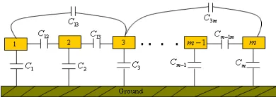
thconductor. The coupling capacitances are illustrated in Fig. 1.
Figure 1. The per-unit length capacitances of a general
m
-conductor transmission lineFor
m
-strip line, the per-unit-length capacitance matrix [C] is given by11 12 1
21 22 2
1 2
[ ]
m
m
m m mm
C
C
C
C
C
C
C
C
C
C
(4)
10 0 0
L
C
(5)where
L
is the inductance matrix,
0the permittivity of free space or vacuum,
0the permeability of free space or vacuum, and
C
0 1the inverse matrix of the capacitance of the multiconductor transmission line when all dielectric constants are set equal one.
3. Results and Discussion
Conductors cannot be considered to have negligible thickness in packaging structures, printed circuit boards and many microwave structures. Their thickness has to be taken into account for the calculation of capacitance in order to give accurate results. The accuracy is essential in studying the interactions of transmission lines to obtain useful information for the ability of the line to transmit signals at high frequencies (in GHz region) with low distortion and minimum crosstalk. Therefore, we choose to use very small thickness (0.01 mm) for all the conductors.
The significant advantages of printed circuits are somewhat offset by the electromagnetic complexity of the structure, because its inherent inhomogeneous nature makes accurate calculations difficult. We compared our results with the integrated equations technique (IET), the method of moment (MoM) and the method of lines (MoL).
In this paper, we consider two different models. First case, investigates the modeling of the shielded two vertically coupled striplines embedded in dielectric material. We identify the quasi-TEM spectral for the potential distribution of the designed model and its mesh. Also, we computed the values of capacitances and inductance per unit length the model. Indeed, we compare the values of capacitances with the other methods. For second case, we illustrate the modeling of shielded two coupled striplines embedded in dielectric material. We identify the quasi-TEM spectral for the potential distribution of the designed model and its mesh. In addition, we computed the values of capacitances and inductance per unit length. Also, we compare the capacitances values with the other methods.
3.1. Shielded Two Vertically Coupled Striplines Embedded in Dielectric Material
In this section, we illustrate the modeling of the shielded two vertically coupled striplines embedded in dielectric material by focusing on the potential distribution and meshing. Furthermore, we compute the capacitance per unit length and inductance per unit length of the coupled striplines.
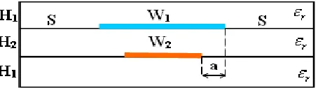
In Figure 2, we show the cross section for shielded two vertically coupled striplines and the geometry is enclosed by a 3.4 X 1mm shield with the following parameters:
r
= dielectric constant = 1and 9.5 W1 = width of the stripline 1 = 1.4mm W2 = width of the stripline 2 = 1mmH1 = height from stripline 1 and stripline 2 to the upper side and lower side of the shield respectively = 0.4mm
H2 = distance between the two striplines = 0.2mm
S = distance between the stripline 1 and right/left side of the shield = 1mm a = (W1-W2)/2 = 0.2mm
t = thickness of the striplines = 0.01mm
From the model, we generate the finite element mesh plot as in Figure 3. Table 1 shows the statistical properties of the mesh.
Figure 3. Mesh plot of the shielded two vertically coupled striplines embedded in dielectric material
Table 1. Mesh statistics of the shielded two vertically coupled striplines embedded in dielectric material
Items Value Number of degrees of freedom 9789
Total Number of mesh points 2260 Total Number of elements 4466 Triangular elements 4466
Quadrilateral 0 Boundary elements 402
Vertex elements 12
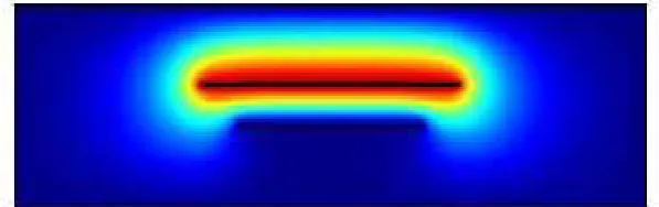
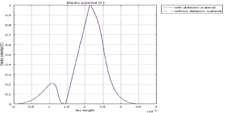
Figure 3 shows the 2D surface potential distribution for the model; while the contour plot is presented in Figure 4. Figure 5 presents the comparison analysis of potential distribution of the model with and without dielectric substrate. It observed that the peak value of electric potential is same as the dielectric is placed in the substrate when we use the first conductor as input.
Figure 3. 2D surface potential distribution of the shielded two vertically coupled striplines embedded in dielectric material
Figure 5. Potential distribution of the shielded two vertically coupled striplines embedded in dielectric material from (x, y) = (0, 0) to (x, y) = (3.4, 1) mm
Table 2 shows the finite element results for the capacitance per unit length of shielded two vertically coupled striplines compared with the work of previous investigation using integrated equation technique (IET) and method of lines (MoL). They are in good agreement.
Table 2. Values of the capacitance coefficient (in F/m) for shielded two vertically coupled striplines in air (
o
8.854 10
12F m
/
)Capacitance IET [Ref. 4] MoL [Ref. 1] Our work
11
/
oC
11.434 11.4142 11.955712
/
oC
-5.954 -5.9672 -6.325621
/
oC
-5.954 -5.9672 -6.325622
/
oC
9.303 9.3305 9.7124We extend the model by computing the capacitance coefficient (in pF/m) and inductance (in
H/m) for shielded two vertically coupled striplines in dielectric material (9.5
r
) as shown in Table 3.Table 3. Values of the capacitance coefficient (in pF/m) and inductance (in
H/m) for shielded two vertically coupled striplines in dielectric material (
r
9.5
)Capacitance Our work Inductance Our work
11
C
1006.015L
11 0.160212
C
-532.3175L
12 0.104321
C
-532.3175L
21 0.104322
3.2. Shielded Two Coupled Striplines Embedded in Dielectric Material
In this section, we illustrate the designing and modeling of the shielded two coupled striplines embedded in dielectric material by focusing on the calculation of capacitance and inductance per unit length. In Figure 6, we show the cross section for shielded two coupled striplines and the geometry is enclosed by a 16 X 3mm shield with the following parameters:
r
= dielectric constant = 9.5 W1 = width of the stripline 1 = 3mm W2 = width of the stripline 2 = 3mmH1 = height from stripline 2 to lower side of the shield = 0.5mm H2 = distance between the two striplines = 0.5mm
H3 = height from stripline 1 to the upper side of the shield = 2mm
S1 = distance between the stripline 1 and right side of the shield and the distance between the stripline 2 and the right side of the shield = 4mm
S2 = distance between the striplines = 2mm t = thickness of the striplines = 0.01mm
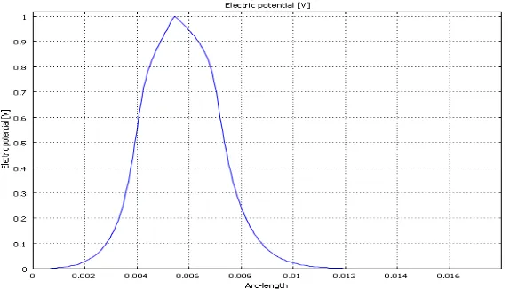
From the model, we generate the finite element mesh plot as in Figure 7. Table 4 shows the statistical properties of the mesh. While, Figure 8 shows the 2D surface potential distribution for the coupled stripline; although the contour plot is presented in Figure 9 of the model. Figure 10 presents the electric potential plot as a function of arc-length.
Figure 6. Cross section of the shielded two coupled striplines embedded in dielectric material
Figure 7. Mesh of the shielded two coupled striplines embedded in dielectric material
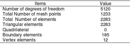
Table 4. Mesh statistics of the shielded two vertically coupled striplines embedded in dielectric material
Items Value Number of degrees of freedom 5120
Total Number of mesh points 1233 Total Number of elements 2283 Triangular elements 2283
Quadrilateral 0 Boundary elements 185
Figure 8. 2D surface potential distribution of shielded two coupled striplines embedded in dielectric material
Figure 9. Contour plot of the potential distribution of shielded two coupled striplines embedded in dielectric material with port 1 as input
Figure 10. Potential distribution of shielded two coupled striplines embedded in dielectric material using port 1 as input along a line from (x, y) = (0, 0) to (x, y) = (16, 3) mm
Table 5 shows the finite element results for the capacitance per unit length of shielded two coupled striplines compared with the work of previous investigations using the method of moment (MoM) and the method of lines (MoL). They are in good agreement.
Table 5. Values of the capacitance coefficient (in F/m) for shielded two coupled striplines material
Capacitance MoM [Ref. 3] MoL [Ref. 1] Our work
11
/
oC
60.4924 59.2746 60.564012
/
oC
-1.0447 -1.0567 -1.174021
/
oC
-1.0447 -1.0567 -1.174022
/
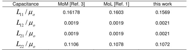
oWe computed inductance per unit length of the model computing and compare the results with the MoM and MoL methods, we found then in excellent agreement as shown in Table 6.
Table 6. Values of the inductance (in H/m) for shielded two coupled striplines in dielectric material
Capacitance MoM [Ref. 3] MoL [Ref. 1] this work
11
/
oL
0.16178 0.1603 0.156912
/
oL
0.0019 0.0019 0.002121
/
oL
0.0019 0.0019 0.002122
/
oL
0.1106 0.1078 0.10724. Conclusion
In this paper, we have presented the quasi–static of two-dimensional shielded two vertically coupled striplines and shielded two coupled striplines embedded in dielectric material using FEM. The results obtained using finite element method for the capacitance per unit length and inductance per unit length agrees well with those found in the other methods. We found them to be very close. In addition, we determine the quasi-TEM spectral for the potential distribution of the models.
References
[1] Zitouni A, Bourdoucen H, Djoudi TN. Quasi-static Mol-based Approach for the Analysis of Multilayer Transmission Line Structures. International Journal of Numerical Modeling: Electronic Networks, Devices and Fields. 1997; 10: 209-216.
[2] Papachristoforos A. Method of Lines for Analysis of Planar Conductors with Finite Thickness. IEE Proc. Microwave Antennas and Propagation. 1994; 141(3): 223-228.
[3] Wei C, Harrington RF, Mautz JR, Sarkar TK. Multiconductor Transmission Lines in Multilayered Dielectric Media. IEEE Transaction on Microwave Theory and Techniques. 1984; 32(4): 439-450. [4] Kammler DW. Calculation of Characteristic Admittances and Coupling Coefficient for Strip
Transmission Lines. IEEE Transaction on Microwave Theory and Techniques.1968; 16(11): 925-937. [5] Li YL, Liu CH. Simplified Green’s Functions for Calculating Capacitance and Inductance of
Multiconductor Transmission Lines in Multilayered Media. IEE Proc. Microwave Antennas and Propagation. 1994; 141(2):141-144.
[6] Bontzios YI, Dimopoulos MG, Hatzopoulos AA. An Evolutionary Method for Efficient Computation of Mutual Capacitance for VLSI Circuits based on the Method of Images. Simulation Modeling Practice and Theory. 2011; 19: 638-648.
[7] Milovanovic A, Kopprivica B. Calculation of Characteristic Impedance of Eccentric Rectangular Coaxial Lines. Przeglad Elektrotechniczny (Electrical Review). 2012; 88: 260-264.
[8] Illias HA, Bakar AHA, Mokhlis H, Halim SA. Calcualtion of inductance and Capacitance in Power System Transmission Lines using Finite Element Analysis Method. Przeglad Elektrotechniczny (Electrical Review). 2012; 88: 278-283.
[9] Musa SM, Sadiku MNO, Clark JV. Finite Element Analysis for Electromagnetic Parameters of Multiconductor Interconnects in Multilayered Dielectric Media. International Journal of Research and Reviews in Computer Science. 2011; 2(6): 1300-1304.
[10] Musa SM, Sadiku MNO. Computer-aided Modeling of Circular Conductors. Microwave and Optical Technology Letters. 2009; 51(5): 1366-1372.