PART
2
Advanced Power Amplifier
Design Techniques
P
art 2 delves deeply into the design of advanced power amplifiers with state-of-the-art performance. Advanced input, VAS, and output stages are discussed in depth, as are DC servos for DC offset control. A complete chapter is devoted to advanced forms of neg-ative feedback compensation that can provide high slew rate and low distortion without compromising stability. A detailed discussion of noise sources is also included in Chapter 7 where input and VAS cir-cuits are covered. Crossover distortion, one of the most problematic distortions in power amplifiers, is studied in depth in Chapter 10. Both static and dynamic crossover distortions are covered. Part 2 also includes a detailed treatment of MOSFET output stages and error cor-rection techniques. Part 2 closes with a discussion of other sources of distortion that are less well known.C
HAPTER 7Input and VAS Circuits
C
HAPTER 8DC Servos
C
HAPTER 9Advanced Forms of Feedback Compensation
C
HAPTER 10Output Stage Design and Crossover Distortion
C
HAPTER 11MOSFET Power Amplifiers
C
HAPTER 12Error Correction
C
HAPTER 13127
CHAPTER
7
Input and VAS Circuits
T
he amplifier that was evolved in Chapter 3 served as a good platform for ampli-fier design understanding, but it did not include significant sophistication of the input stage (IPS) and voltage amplifier stage (VAS) circuits. Rather, it started with the most basic IPS-VAS and evolved it in a linear way to achieve much-improved performance. Although the end result was quite good, there are many ways to skin a cat and achieve further improved performance. Moreover, the analysis of the IPS-VAS was fairly superficial, for example, there was little discussion of noise.7.1 Single-Ended IPS-VAS
The single-ended IPS-VAS was discussed at length in Chapter 3 where a basic amplifier was evolved to a high-performance amplifier. Most of the evolution in the design took place in the IPS-VAS. It is referred to as single ended because the VAS is single ended with a current source load. Later in this chapter we will focus on designs that include a push-pull VAS for improved performance.
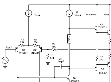
The IPS-VAS shown in Figure 7.1 is unlike the simple IPS-VAS that was used as a starting point in Chapter 3. It is provided with ±45-V rails that correspond to an ampli-fier capable of delivering about 100 W into an 8-W load. This IPS-VAS includes emitter degeneration and is arranged with output stage predrivers and drivers as if a Triple EF was being used for the output stage. The output stage is not present, and the feedback is taken from a center tap on the driver emitter bias resistor. This allows distortion of the IPS-VAS to be evaluated in the absence of the distortion of an output stage.
The pair of 234-W emitter degeneration resistors implements 10:1 degeneration of the input differential pair by increasing the total emitter-to-emitter resistance RLTP from 52 W to 520 W. This reduces its transconductance by a factor of 10.
Recall the relationship described in Chapter 2 for Miller compensation:
CMiller= 1/(2 pfc RLTP Acl)
where Acl is the closed-loop gain, RLTP is the total emitter-to-emitter LTP resistance including re’, and fc is the desired gain crossover frequency for the negative feedback loop. Setting fc to 500 kHz and closed-loop gain to 20, we have
C1 =CMiller= 0.159/(500 kHz * 520 W* 20) = 30.6 pF
By this calculation C1 must be about 30 pF.
Improved Single-Ended IPS-VAS
The IPS-VAS shown in Figure 7.2 is very much like the last one shown in Chapter 3 that was evolved to a high-performance level. The major improvements made to that design included a current mirror load on the IPS and a Darlington-cascode VAS with current limiting. This combination of improvements greatly increased the open-loop gain while virtually eliminating the Early effect in the VAS.
Figure 7.3 plots 20-kHz THD as a function of output level for the IPS-VAS circuits of Figures 7.1 and 7.2. One can see the great improvement in performance achieved by merely adding a few small-signal transistors to the circuit. Bear in mind that this distor-tion does not include output stage distordistor-tion. Isolating the IPS-VAS distordistor-tion is the best way to compare different designs of this portion of an amplifier.
Shortcomings of the Single-Ended IPS-VAS
The ended IPS-VAS is asymmetrical. With a 10-mA quiescent current, the single-ended VAS can never source more than 10 mA to the output stage. However, it can sink an amount of current that is limited only by whatever current limiting is built into the VAS. The transconductance of the single VAS transistor varies in accordance with the amplitude and polarity of the output current. When the VAS is sourcing high current to the output stage, the VAS transistor is operating at a low collector current, and its transcon-ductance is correspondingly low. When the VAS is sinking high current from the output
stage, the VAS transistor is operating at high current and has high transconductance. Such signal-dependent changes in transconductance lead to open-loop gain variations that are dependent on the signal in such a way as to cause second harmonic distortion. The degen-eration of the VAS mitigates this problem but does not eliminate it.
A VAS design in which the Early effect can play a significant role will suffer second harmonic distortion from the Early effect as well, since the current gain and output impedance of the VAS will depend on the output signal voltage.
Perhaps the single biggest improvement that can be made to the VAS is to make it push-pull, replacing the current source load with a second common emitter VAS sistor that is driven with a signal of polarity opposite to that driving the first VAS tran-sistor. This makes the VAS symmetrical, providing equal sourcing and sinking current capabilities and canceling most effects that create second harmonic distortion. The transconductance of the VAS is doubled because it becomes the sum of the transcon-ductances of the positive and negative VAS transistors. When one transistor’s gm is
high, the gm of the other one is low. For a given quiescent current, the maximum avail-able VAS output drive current is doubled.
Most of the IPS-VAS variations that will be seen in this chapter simply reflect differ-ent approaches to delivering the necessary drive signal to the added complemdiffer-entary VAS transistor.
Opportunities for Further Improvement
Many variations on the IPS and VAS are possible. Some provide improved symmetry and performance, while others bring functional features like Baker clamps to control clipping behavior. Others simply represent alternative approaches to the IPS-VAS that some believe sound better or are more immune to things like EMI ingress.
Input Stage Stress
Input stage distortion cannot be ignored. Some IPS-VAS architectures will increase or decrease the susceptibility of the amplifier to distortion that originates in the IPS. Per-haps the most well known effect is high-frequency distortion caused by increased error signal input amplitude at high frequencies. This distortion is associated with transient
intermodulation distortion (TIM) and slewing-induced distortion (SID) [1, 2, 3, 4]. Input
stage distortion is reduced, but not eliminated, by input stage degeneration.
The size of the error signal presented to the input stage is a measure of input stage stress that results in input stage distortion. For a given output signal amplitude, the input stage stress is inversely proportional to the open-loop gain for a sinusoidal signal. In a typical amplifier design with dominant pole compensation, the open-loop gain is smaller at high frequencies (like 20 kHz), leading to greater input stage stress. At low
0.1 0.0001
0.001
THD-20, %
Power Output, W 0.01
0.1
1.0 10 100
Figure 7.1
Figure 7.2
frequencies, the open-loop gain is substantially higher, leading to substantially reduced input stage stress. Amplifiers with wide loop bandwidth have the same open-loop gain at low and high audio frequencies and thus place just as much stress on the input stage at low frequencies as they do at high frequencies.
Amplifiers with low amounts of negative feedback (and thus low open-loop gain) across the audio band subject the input stage to correspondingly greater input stage stress. Amplifiers with no global negative feedback have open-loop gain simply equal to the amplifier gain; this means that the full amplitude of the line level input signal is applied to the input stage, creating the greatest stress and demanding the design of an input stage that is very linear up to high input signal levels. This requires an input stage with very high dynamic range.
There is one caveat to the above observations. The error signal applied to the input stage in amplifiers with high open-loop gain at low frequencies is essentially a differenti-ated version of the input signal. If the amplifier is driven with a square wave, the peak error signal under some conditions can approach the peak-to-peak value of the input sig-nal, implying an error signal swing that could in theory be twice as large as the case where open-loop gain was uniform across the bandwidth to which the square wave is limited.
7.2 JFET Input Stages
A popular alternative to the BJT input differential pair is the JFET input pair. This choice has advantages and disadvantages. Many believe that the sound is better while others believe that its superior resistance to input EMI is important. JFETs usually have increased input referred voltage noise, but in power amplifier applications this is not a serious issue due to the line-level signal voltages involved. Moreover, JFETs have virtu-ally no input current noise. When a BJT-LTP is degenerated to the same transconduc-tance as a JFET (to help slew rate, for example), the noise contributed by the emitter degeneration resistors will often increase the input voltage noise of the BJT stage to be similar to that of the JFET stage.
In the strictest sense, the gm of a JFET-LTP is not as linear as that of a BJT-LTP degen-erated to the same low value of transconductance. However, the cutoff characteristic of a BJT pair is much sharper. Figure 7.4 shows a comparison of the differential pair trans-fer characteristic for BJT and JFET input pairs that have the same small-signal transcon-ductance. For the JFET differential pair, the device is the Linear Systems LS844 operating with a tail current of 2 mA and with gm of about 2.0 mS for each transistor. The BJT-LTP operates at a tail current of 1 mA and is degenerated by a factor of 10 with 470-W emitter resistors to bring its transconductance down to the same 2 mS. Both LTPs are loaded with a current mirror.
Figure 7.5 shows THD-1 as a function of signal level for the same two input stages. The bottom two traces show the sum of fifth- and seventh-order harmonics for these stages, giving an idea of the relative levels of the less benign higher-order harmonics.
JFET Transistors
JFETs operate on a different principle than BJTs. Picture a bar of n-type doped silicon connected from source to drain. This bar will act like a resistor. Now add a pn junction somewhere along the length of this bar by adding a region with p-type doping. This is the gate. As the p-type gate is reverse biased, a depletion region will be formed, and this will begin to pinch off the region of conductivity in the n-type bar. This reduces current flow. This is called a depletion-mode device. The JFET is nominally on, and its degree of
–2.0 –1.5
BJT-LTP
–2.0 –1.5 –1.0 –0.5 0.0
Vin
0.5 1.0 1.5 2.0 JFET-LTP
–1.0 –0.5 0.0
Vout
0.5 1.0 1.5 2.0
FIGURE 7.4 Transfer characteristics for BJT and JFET differential pairs with the same transconductance.
JFET 5th JFET
THD
Input Level, Vpk
0.01 0.001
0.01 0.1
THD-1, %
1.0 10
0.1 1.0
BJT 5th BJT THD
conductance will decrease as reverse bias on its gate is increased until the channel is completely pinched off.
The reverse gate voltage where pinch-off occurs is referred to as the threshold voltageVt. The threshold voltage is often on the order of –.5V to –4V for most small-signal N-channel JFETs. Note that control of a JFET is opposite to the way a BJT is controlled. The BJT is normally off and the JFET is normally on. The BJT is turned on by application of a forward bias to the base-emitter junction, while the JFET is turned off by application of a reverse bias to its gate-source junction.
The reverse voltage that exists between the drain and the gate can also act to pinch off the channel. At Vdg greater than Vt, the channel will be pinched in such a way that the drain current becomes self-limiting. In this region the JFET no longer acts like a resistor, but rather like a voltage-controlled current source. These two operating regions are referred to as the linear region and the saturation region, respectively. JFET amplifier stages usually operate in the saturation region.
JFET
I
dversus
V
gsBehavior
Figure 7.6a shows how drain current changes as a function of gate voltage in the satura-tion region; Figure 7.6b illustrates how transconductance changes as a funcsatura-tion of drain current in the same region. The device is one-half of a Linear Systems LS844 dual JFET. Threshold voltage for this device is nominally about –1.8 V.
The JFET I-V characteristic (Id versus Vgs ) obeys a square law, rather than the expo-nential law applicable to BJTs. The simple relationship below is valid for Vds > VT and does not take into account the influence of Vds that is responsible for output resistance of the device.
Id=β(Vgs – Vt)2 (7.1)
The equation is valid only for positive values of Vgs – Vt. The factor β governs the transconductance of the device. When Vgs=Vt, the Vgs – Vt term is zero and no current flows. When Vgs= 0 V, the term is equal to Vt2 and maximum current flows.
The maximum current that flows when Vgs= 0 V and Vds >> Vt is referred to as IDSS, a key JFET parameter usually specified on data sheets. Under these conditions the chan-nel is at the edge of pinch off and the current is largely self-limiting. In this case it is the reverse bias of the gate junction with respect to the drain that is pinching off the chan-nel. The parameter β is the transconductance coefficient and is related to IDSS and Vt. The value of IDSS for the LS844 is about 3.1 mA, and the value of β is about 0.9 mA/V2.
β=IDSS/Vt2 (7.2)
The parameter β can also be expressed in mS/V; this means that if gm is plotted as a function of Vgs, a straight line will result. With some manipulation of Eq. 7.1, it can be seen that the transconductance of the JFET is proportional to the square root of the drain current.
gm=2 βId (7.3)
0.0 mA
–2.0 –1.8 –1.6 –1.4 –1.2 –1.0 –0.8 –0.6 –0.4 –0.2 –0.0 0.5 mA
1.0 mA 1.5 mA 2.0 mA 2.5 mA 3.0 mA 3.5 mA
0.0 mS
0.0 0.2 0.4 0.6 0.8 1.0 1.2 1.4 1.6 1.8 2.0
0.5 mS 1.0 mS 1.5 mS 2.0 mS 2.5 mS
Id
Id, mA
gm
Vgs, V
(b) (a)
3.0 mS
LS844
Id vs. Vgs
LS844
gm vs. Id
FIGURE 7.6 (a) JFET drain current as a function of gate voltage. (b) Transconductance as a
Id= 1 mA is about 2 mS. The gm of a BJT at Ic= 1 mA is about 40 mS, greater by a factor of 20. The larger LSK389 has Vt= – 0.54 V, IDSS = 8.4 mA, and gm of 11.3 mS at 1 mA.
The JFET turn-on characteristic is much less abrupt that that of a BJT. Absent degen-eration of a BJT, the input voltage range over which the JFET is reasonably linear is much greater than that of a BJT. The collector current of the BJT increases by a factor of about 2 for every increase of 18 mV in Vbe. Between 0.75 mA and 1.5 mA, Vgs of an LS844 changes by about 370 mV.
JFET RFI Immunity
When operating in the quiescent state, the gate-source junction of the JFET is typically reverse biased by a volt or two. In contrast, the base-emitter junction of the BJT is forward biased by about 600 mV. This means that the latter is more prone to rectification effects at its base-emitter junction, making the un-degenerated BJT far more prone to RFI pickup, demodulation, and intermodulation. A degenerated BJT is less prone to this effect because it has a higher signal overload voltage as a result of the emitter degeneration.
Voltage Ratings
JFETs often do not have as high a voltage rating as BJTs, and this sometimes requires that JFET input stages be cascoded. The LSK389, for example, has maximum Vds of only 40 V. Most of the voltage drop required in an IPS can be accommodated by the addition of BJT cascode transistors. Figure 7.7 illustrates a JFET-IPS that can handle the rail voltages encountered in a typical power amplifier. Each LS844 JFET is operated at a drain current of 1 mA, and its drain is loaded by a BJT cascode whose bases are biased at +15 V.
The JFETs employed are the Linear Systems monolithic dual-matched LS844 devices. These devices are matched to within ±5 mV and have typical input-referred noise of
3 nv/ Hz. The 2-mA tail current for the JFETs is required to bring their transconductance
up to that of the degenerated BJTs in Figure 7.2. This means that the Miller compensation capacitor can remain of the same value. Note, however, that slew rate will be doubled as a result of the doubled tail current for the JFETs.
JFET Input Pairs and Matching
The threshold voltages among discrete JFETs can be quite different, so it is virtually mandatory to employ monolithic dual-matched pair devices. While discrete P-channel JFETs are readily available, dual-matched pairs like the Toshiba 2SK389/2SJ09 are scarce and largely no longer in production. That is why the IPS-VAS of Figure 7.7 is upside down from the BJT version of Figure 7.2. N-channel matched JFET pairs are better per-forming and much more readily available.
Some IPS-VAS circuits use a full-complementary IPS-VAS with two pairs of JFET-LTPs, one N-channel, and one P-channel. The scarcity of P-channel matched pairs makes this kind of IPS difficult to build in practice. It is also true that the P-channel matched pairs, when available, may not be well matched to the N-channel complements for transconductance at a given operating current.
7.3 Complementary IPS and Push-Pull VAS
The VAS designs illustrated in Chapter 3 were all of a single-ended drive nature, where the large voltage swing at the output of the VAS was developed by a common-emitter stage loaded by a constant current source. In those examples, the maximum amount of pull-up current on the VAS output node was limited to the value of the current source, which in turn was equal to the idle current of the VAS. The pull-down current would not be limited in the same way. The collector current of the VAS transistor would be smaller when the output node was being pulled up and larger when the output node was being pulled down. This in turn meant that the transconductance of the VAS tran-sistor would be different under these two conditions. This asymmetrical structure and behavior of the VAS can lead to second harmonic distortion and other performance impairments.
The push-pull VAS addresses these limitations by employing active common-emitter VAS transistors of each polarity, one pulling up and one pulling down. Such a sym-metrical architecture has many advantages. Twice the peak drive current is available for a given VAS quiescent current and the symmetry suppresses the creation of second harmonic distortion.
The key challenge with the push-pull VAS is how to drive the two common-emitter VAS transistors, one referenced to the positive rail and the other referenced to the nega-tive rail. In the approaches described in this section, two input pairs are employed, one a PNP-LTP and one an NPN-LTP. P-channel and N-channel JFET-LTPs can be used also. The PNP-LTP provides drive to the VAS transistor on the bottom while the NPN-LTP drives the PNP-VAS transistor on the top. A simplified version of an IPS-VAS using this approach is illustrated in Figure 7.8.
way to drive a push-pull VAS and, if nothing else, has appealing symmetry on the sche-matic. Many of the usual IPS-VAS improvements can be applied to the arrangement of Figure 7.8, such as Darlington-connected VAS transistors.
Complementary IPS with Current Mirrors
We saw in Chapter 3 the great improvement that resulted from employing current mirror loads on the IPS-LTP. Such an approach is illustrated in Figure 7.9. Here there is a current mirror on top driving the PNP-VAS transistor and another current mirror on the bottom driving the NPN-VAS transistor. Both current mirrors enable the input stage to provide high gain, especially given that both of the VAS transistors employ a Darlington connection. Look at the circuit and see if you can calculate the VAS quiescent current from the components and currents shown. You can’t. That is the problem with this circuit. The VAS quiescent current is indeterminate. This is not a practical and reliable circuit. Some means must be introduced to establish some reliability with the VAS bias current. Such a means will cause the output volt-age of the current mirror to be at a defined level when the LTP is in balance.
One approach to solving this problem is illustrated in Figure 7.10. First notice that each current mirror has had a helper transistor added to it (Q13, Q14). This is little more than an emitter follower that supplies the base current for the current mirror transistors,
rather than having it drained from the incoming current. This improves DC balance of the current mirror and greatly decreases the influence of transistor beta on its operation.
Notice also that the helper transistor separates the voltage at the current mirror input (collector of Q6) by one additional Vbe from the rail. This puts that voltage 2Vbe
plus the drop across R6 away from the rail. This happens to be the same voltage drop from the rail as exists at the input to the Darlington VAS transistor if Vbe drops are the same and amount of degeneration voltage drop is the same.
Resistor R14 connected across the collectors of Q1 and Q2 accomplishes the remain-der of solving the problem. When the LTP is in balance, no current flows through R14; the voltage on both sides is the same. The voltage at the emitter of the VAS transistor then becomes approximately the same as the voltages at the emitters of the current mirror transistors, which are set by the LTP tail current. It is easily seen that the quiescent current of the VAS is now established so that it depends directly on the tail current in the LTPs.
FIGURE 7.9 Complementar y differential input stage with current mirror loads suffers quiescent
The price being paid here is a slight reduction in the gain of the input stage. It is differentially loaded by R14 instead with very high indeterminate impedance set by transistor betas. The effective load resistance is half the value of R14, since the current flowing through R14 is recirculated through the current mirror to further oppose volt-age change at the output of the current mirror. The value of the differential shunt resis-tor can be quite high if well-balanced circuitry is used with precision resisresis-tors.
This circuit is sensitive to differences in the tail currents for the NPN and PNP LTPs. It can be seen that any such difference will attempt to set a different quiescent current for the top and bottom halves of the VAS. This cannot be, so an input offset voltage will be created for the overall stage that forces the top and bottom VAS transistors to operate at the same current.
Complementary IPS with JFETs
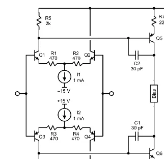
Many fine amplifiers have been made with the complementary IPS using JFETs, as illus-trated in Figure 7.11. All of the same approaches and caveats apply. The JFET-LTPs are cascoded to keep the drain voltages of the JFETs at suitable levels.
There are two concerns that apply with complementary JFET input stages. First and foremost, P-channel dual-matched JFETs are very difficult to find. Few, if any, are still in production as of this writing. Secondly, the transconductance of the P-channel pair does not match that of the N-channel pair at the same operating current without painstaking selection of devices.
Complementary IPS circuits do not perform well if the transconductances of the top and bottom halves are not well matched; each half will have different gain, and the top and bottom parts of the VAS will tend to fight each other. This results in second har-monic distortion. This is especially so if twin Miller compensation capacitors are used as shown. Each compensation capacitor creates a shunt feedback loop that makes the
output impedance of its half of the VAS low. Two low-impedance sources connected in parallel (the top and bottom halves of the VAS) will fight each other unless each one is trying to put out the exact same voltage as the other one. If the transconductances of the top and bottom LTPs are not the same, this condition will not be satisfied. Optional emitter degeneration resistor pairs R1-R2 and R3-R4 can be set to different values in order to better equalize the transconductances of the top and bottom LTPs.
Floating Complementary JFET-IPS
An elegant complementary JFET-IPS popularized by John Curl floats the complemen-tary differential pairs. An arrangement like this is shown in Figure 7.12. This design takes advantage of the depletion mode biasing of the JFETs to create what is effectively a floating common current source for the N-channel and P-channel LTPs. The sum of the
Vgs voltages of the top and bottom JFET pairs at the chosen operating current is forced to
appear across bias resistor R5 connecting the two pairs, thus establishing the tail cur-rents, which will be equal. Optional source degeneration resistor pairs R1-R2 and R3-R4 can be used to help equalize top and bottom LTP transconductances. The resistances of any degeneration resistors must be taken into account in choosing the value of R5.
The tail current in this design will depend directly on the threshold voltages of the JFET pairs, so some selection or adjustment of R5 may be necessary to arrive at the desired tail current.
Complementary IPS with Unipolar JFETs
The relative unavailability of P-channel dual-matched JFETs makes it tempting to pur-sue an input stage which uses only N-channel JFETs but which still is able to create output signal currents that face both upward and downward.
This is made possible by the circuit shown in Figure 7.13. The N-channel JFETs (Q1, Q2) still act as a differential pair in the upward direction, but their source currents are
harvested with a pair of PNP cascode transistors in their source circuit (Q3, Q4). The
col-lector currents of these cascode transistors flow downward to a current mirror to drive the NPN-VAS transistor. Resistors R1 and R2 provide the degeneration. If one assumes that the base line connecting Q3 and Q4 floats, it is easy to see that the dif-ferential input voltage creates a current that flows through the loop created by Q1, R1, Q3, Q4, R2, and Q2.
The key to making this arrangement work is to get the right bias currents to flow without interfering with common mode rejection. This involves properly generating the voltage at the interconnected bases of Q3 and Q4. This voltage must float with the common mode input voltage and be offset downward by the proper amount to estab-lish the desired bias current. Transistors Q5 and Q6 perform this function.
Q5 and Q6 are emitter followers whose output is summed by R3 and R4 to form a replica of the common-mode voltage. This replica is applied to the bases of Q3 and Q4. Current source I1 provides the necessary pull-down bias current for the emitter follow-ers. Notice that the Vbe drops of Q3 and Q5 cancel each other, as do those of Q4 and Q6. As a result, the voltage drop across R1 and R3 are equal if all Vbe drops are equal. Like-wise, the voltage drop across R2 is the same as that across R4. The DC voltage drops across R1 and R2 set the bias current, and the drop across R3 and R4 is controlled by current source I1. If R3 and R4 equal R1 and R2, then the bias current flowing in Q1 will be equal to one-half I1. Current I1 is the “tail current” of the arrangement.
The arrangement is completed with upper cascode transistors Q7 and Q8. Current mirrors at the top and bottom (Q9, Q10, Q11 and Q12, Q13, Q14) provide the loading. R11 and R12 provide differential loading on the current mirror outputs to provide VAS quiescent current stability.
7.4 Unipolar Input Stage and Push-Pull VAS
The relative scarcity of complementary JFET pairs also makes it desirable to have designs that require only a conventional LTP of one polarity (usually N-channel JFET) while still being able to drive a push-pull VAS. The key to achieving this is how to turn around the signal drive for the opposite side of the VAS. Tom Holman’s APT-1 power amplifier is a good example of this design approach (wherein NPN BJT devices were used) [5].
the LTP output is reflected down to the negative rail where it is used to drive the NPN-VAS transistor. A cascode transistor is placed in the path of the reflected current so as to reduce quiescent voltage on Q6. This architecture does not appear to lend itself well to the use of LTP current mirror loads in the way that they were employed in some earlier arrangements.
Differential Pair VAS with Current Mirror
A slightly different approach is illustrated in Figure 7.15. Here the PNP VAS is actually a differential pair. It is fed from an IPS with a current mirror load, so high gain and good
DC balance is achieved in the IPS. The VAS LTP is fed from both outputs of the IPS, but because of the current mirror arrangement only the IPS output from Q3 has significant voltage movement. The IPS output from Q4 acts as a voltage reference for the other input of the VAS LTP. Diodes D1 and D2 prevent the current mirror transistors from saturating when the amplifier clips. The PNP VAS LTP (Q10, Q11) is preceded by NPN emitter fol-lowers Q8 and Q9. Their Vbe drops cancel those of the LTP transistors. The LTP is powered by twin current sources and its gain is set by R8 connected between the emitters of Q10 and Q11. The twin current source arrangement helps conserve voltage headroom because the VAS bias current does not flow through the emitter degeneration resistance.
The bottom half of the VAS is formed by a current mirror (Q13, Q14, Q15). A cascode (Q12) is situated in the path of the current from Q10 to the current mirror to share the voltage drop that spans both supply rails. Conventional Miller compensation is pro-vided by C1 connected from the collector of Q11 to the base of Q9. A further advantage of this design is that the VAS is naturally current limited; it can never sink or source more than the total amount of its LTP tail current.
IPS with Differential Current Mirror Load
A more advanced form of unipolar IPS-VAS front end is shown in Figure 7.16. This arrangement was used in Ref. 6. The key advantage of this circuit is that it allows the
use of a balanced current mirror structure to load the input stage. The differential cur-rent mirror exhibits very high impedance in the diffecur-rential mode, but rather low imped-ance in the common mode. It thus provides some additional common-mode rejection. The primary elements of the differential current mirror are current sources Q5 and Q6. Emitter followers Q7 and Q8 jointly act as the current mirror helper transistors, creating and feeding back a common mode voltage to control current sources Q5 and Q6. The emitter followers also buffer the differential signal before application to the VAS LTP.
The differential current mirror establishes a well-defined common-mode voltage level to be applied to the VAS LTP. This, combined with the differential drive of the LTP, allows the use of a simple resistor tail for Q9 and Q10. The VAS in Figure 7.16 also employs cascodes Q11 and Q12, suppressing the Early effect and allowing the use of fast, low-voltage transistors for Q9 and Q10. The bias voltage provided for the cascodes is also used to power emitter followers Q7 and Q8, again allowing the use of fast, low-voltage transistors. A similar approach is used for the cascoded current mirror Q14-Q17.
Diodes D1 and D2 clamp the IPS differential output voltage to prevent saturation of Q5 and Q6 when the amplifier clips. This IPS-VAS is best used with Miller input
compen-sation (MIC) as implemented by C1 and R18. MIC will be described in Chapter 9. The
series R-C network across the IPS collectors (C2 and R5) provides some lag-lead fre-quency compensation for the high-impedance intermediate nodes between the IPS and
VAS. This compensates the local MIC feedback loop. In some MIC implementations an additional series R-C network is required from the VAS output to ground.
7.5 Input Common Mode Distortion
In the customary noninverting amplifier configuration the full line-level input signal is applied to the input stage as a common mode signal. This can create distortion in a number of ways. Since this distortion makes itself apparent as an effective input- referred differential signal at the input stage, negative feedback cannot reduce it.
One source of common-mode distortion can originate in the tail current source. A cas-coded current source can reduce this contributor. Another problem can arise from the Early effect in the LTP transistors. At high frequencies the nonlinear collector-base capacitance of the LTP transistors can also introduce common-mode distortion, especially if the imped-ances of the networks driving the LTP are not very low. An IPS with a single-ended output and not loaded by a current mirror is more vulnerable to common-mode distortion. In some cases JFETs may be more susceptible to common-mode distortion than BJT devices.
Input common-mode distortion can be reduced with a driven cascode. Figure 7.17 shows how an input stage cascode can be driven with a replica of the common-mode signal, making the collector-base voltage of the LTP transistors constant, independent of signal. The replica is formed by passing the amplifier output signal through a second feedback network formed by R3 and R4. Other approaches to generating the common-mode signal for driving the cascode are also possible. For example, the tail signal of the LTP can be buffered and level shifted as needed.
7.6 Early Effect
As discussed in Chapters 2 and 3, the current gain of a transistor is mildly dependent on the collector voltage. This leads to a finite output resistance in a common-emitter stage, and unfortunately this resistance is nonlinear. It was shown that the use of a cas-code VAS greatly reduces this effect, but does not eliminate it completely. The usual cascode fixes the potential at the collector of the common-emitter stage, so that signal voltage at the base still modulates Vbc.
There is also the Early effect at the input to the driver or predriver transistors of the output stage. This is because the base-collector voltage of the driver transistor is modu-lated by the signal, and thus its beta is influenced via its Early effect. The bias current flowing through the driver, even if constant, will result in a changing base current for
the driver. The shunt feedback provided by the usual Miller compensation will reduce the output impedance of the VAS, and this will also reduce the influence of the Early effect.
7.7 Baker Clamps
When amplifiers are overdriven, they will clip. How cleanly they clip can have an effect on the sonic performance of the amplifier. How often amplifiers clip depends on many factors, not the least of which include loudspeaker efficiency and the crest factor of the program material being played. In some cases, amplifiers may clip more often than we think. When they do, it is important that they clip cleanly.
In the VAS circuits we have seen thus far, if the amplifier is driven to clipping, the VAS transistor will almost certainly go into saturation. This occurs when the collector voltage goes so low that the base-collector junction becomes forward-biased. Transistors tend to be slow to come out of saturation, and this can lead to a phenomenon called sticking.
A Baker clamp is a diode-based circuit that prevents the signal excursion from going far enough to allow the protected transistors to saturate. A Baker clamp can be as simple as a diode connected to a fixed voltage reference. Baker clamps and related circuitry to control amplifier behavior in the real world are discussed in Chapter 17.
7.8 Amplifier Noise
This section is not intended to be a thorough coverage of noise, but rather to introduce a basic understanding of it. Although the noise characteristics of a power amplifier are not as critical as those of a preamp, it is still important to achieve low noise because there is no volume control in the power amplifier to reduce noise from the input stage under normal listening conditions. This is particularly so when the amplifiers are used with high-efficiency loudspeakers. Here we will explore the way in which noise is gov-erned by the circuits and discuss ways to minimize it.
Power amplifier noise is usually specified as being so many dB down from either the maximum output power or with respect to 1 W. The former number will be larger by 20 dB for a 100-W amplifier, so it is often the one that manufacturers like to cite. The noise referenced to 1 W into 8 W (or, equivalently 2.83 V RMS) is the one more often measured by reviewers.
The noise specification may be unweighted or weighted. Unweighted noise for an audio power amplifier will typically be specified over a full 20-kHz bandwidth (or more). Weighted noise specifications take into account the ear’s sensitivity to noise in different parts of the frequency spectrum. The most common one used is A weighting, illustrated in Figure 7.18. Notice that the weighting curve is up about +1.2 dB at 2 kHz, whereas it is down 3 dB at approximately 500 Hz and 10 kHz.
Noise Power
Noise Bandwidth
Most noise sources have a flat noise spectral density, meaning that there is the same amount of noise power in each hertz of frequency spectrum. This means that total noise power in a measurement is proportional to the bandwidth of the measurement being made. This gives rise to the concept of noise bandwidth.
A perfect brick-wall filter would have a noise bandwidth equal to its signal band-width. Because real filters roll-off gradually, the noise bandwidth is slightly different than the 3-dB bandwidth of a filter (often slightly more). A 12.7-kHz single-pole LPF has
an equivalent noise bandwidth (ENBW) of 20 kHz. Conversely, the ENBW of a 20-kHz
first-order LPF is 31.4 kHz. The ENBW of a single-pole roll-off is equal to 1.57 times the pole frequency. The ENBW of the A-weighting function is 13.5 kHz.
Noise Voltage Density
White noise has equal noise power in each hertz of bandwidth. If the number of hertz is
doubled, the noise power will double, but the noise voltage will increase by only 3 dB or a factor of 2. Thus noise voltage increases as the square root of noise bandwidth, and noise voltage is expressed in nanovolts per root hertz (nV/ Hz). There are 141 Hz
in a 20-kHz bandwidth. A 100-nV/ Hz noise source will produce 14.1 µV RMS in a 20-kHz measurement bandwidth.
As an aside, so-called pink noise has the same noise power in each octave of band-width. Pink noise is usually employed in certain test measurements. Pink noise is created by passing white noise through a low-pass filter having a 3 dB per octave roll-off slope.
Relating Input Noise Density to Signal-to-Noise Ratio
Most of the noise in an amplifier is usually contributed by the input stage or other early stages. For this reason, the noise of an amplifier is often referred back to the input. Input-referred noise is calculated by measuring the output noise and dividing it by the gain of the amplifier. A good op amp might have input-referred noise of 2 nV/ Hz.
If an amplifier has 10 nV/ Hz of input-referred noise, what is its signal-to-noise ratio
(SNR)? Assume that the SNR is in an unweighted 20-kHz bandwidth and that it is referred to 2.83 V RMS out. Also assume that the amplifier has a voltage gain of 20. The output noise voltage will be 10nV/ Hz*141 Hz*20 28 2= . µV. This is 100,000 times smaller than 2.83 V, so the SNR is 100 dB.
Now consider a wideband unweighted noise measurement of the same amplifier. Assume the amplifier has a closed-loop bandwidth of 500 kHz with a single-pole roll-off. The ENBW will be 785 kHz (886 Hz), and the output noise will be 177 µV RMS. The SNR will be 16,000, corresponding to about 84 dB.
A-Weighted Noise Specifications
The frequency response of the A-weighting curve is shown in Figure 7.18. It weights the noise in accordance with the human ear’s perception of noise loudness.
SNR of 105 dB with respect to 1 W. A fair amplifier might sport 65-dB and 80-dB SNR figures, respectively. The A-weighted number will sometimes be 10-20 dB better than the unweighted number.
VAS Noise
The input stage is not the only source of noise in an amplifier, even though it often dominates. Later stages create noise, and their input-referred noise can be referred back to the input of the amplifier by the voltage gain that precedes them. For example, a VAS with input noise of 30 nV/ Hz will contribute an amplifier input-referred noise compo-nent of 10 nV/ Hz if the voltage gain of the input stage is 3. The message here is that VAS noise cannot be ignored, and may even dominate the noise in some amplifier designs. This can happen because the VAS is not usually designed for low noise and input stage gain is sometimes quite small.
Power Supply Noise
The power supply rails in any amplifier are often corrupted by numerous sources of noise. These may include random noise and other noises like power supply ripple and EMI and program-dependent noise from the output stage. The power supply noise can get into the signal path as a result of the signal circuit’s limited power supply rejection ratio (PSRR).
There are two important ways to control power supply noise. The first is to do a better job filtering the power supply rails. This is especially effective for power supply rails that provide power to low-level circuits. The second is to employ circuit topologies that have inherently high PSRR. The ability of a circuit to reject power supply noise usu-ally decreases as the frequency of the noise increases. In other words, PSRR degrades at high frequencies. Fortunately, it is often possible to do a more effective job of filtering the power supply rails at higher frequencies.
Resistor Noise
All resistors have noise. This is referred to as Johnson noise or thermal noise. It is the most basic source of noise in electronic circuits. It is most often modeled as a noise voltage source in series with the resistor. The noise power in a resistor is dependent on temperature.
Pn= 4kTB W = 1.66 × 10⁻²⁰ W/Hz (7.4)
where k= Boltzman’s constant = 1.38 × 10⁻²³ J/°K
T= temperature in °K = 300°K @ 27°C
B= bandwidth in hertz
The open-circuit RMS noise voltage across a resistor of value R is simply
en= 4kTRB (7.5)
en=0 129. nV/ Hz per W (7.6)
Noise voltage for a resistor thus increases as the square root of both bandwidth and resistance. A convenient reference is the noise voltage of a 1-kW resistor:
1kW =>4 1. nV/ Hz
From this the noise voltage of any resistance in any noise bandwidth can be estimated.
Shot Noise
Bipolar transistors generate a different kind of noise. This noise is related to current flow and the discreteness of current. This is called shot noise and is associated with the current flows in the collector and the base of the transistor. The collector shot noise cur-rent is usually referred back to the base as an equivalent input noise voltage in series with the base. It is referred back to the base as a voltage by dividing it by the transcon-ductance of the transistor. Once again, the resulting input-referred noise is usually mea-sured in nanovolts per root hertz.
The shot noise current is usually stated in picoamperes per root hertz (pA/ Hz)
and has the RMS value of
Ishot= 2qI Bdc (7.7)
Ishot=0 57. pA/ Hz/ µA (7.8)
where q= 1.6 × 10⁻¹⁹ Coulombs per electron.
B= bandwidth in hertz
It is easily seen that shot noise current increases as the square root of bandwidth and as the square root of current. An 1-mA collector current flow will have a shot noise component of 18 pA/ Hz.
1mA=>18pA/ Hz
At the same time, notice that re’ for this transistor is 26 W. The noise voltage for a 26-W resistor is 0 66. nV/ Hz. The input-referred voltage noise of a transistor is equal to the Johnson noise of a resistor of half the value of re’. This is a very handy relationship.
BJT Input Noise Current
The base current of a transistor also has a shot noise component measured in units of
pA/ Hz. Recall that
Ishot=0 57. pA/ Hz/ µA (7.8)
Consider a BJT biased at 1 mA and with a beta of 100. Base current will be 10 µA. This corresponds to 3 16. µA. Input noise current will be 1 8. pA/ Hz. Put another way, base shot noise is collector shot noise divided by β.
If the base circuit includes source resistance, the base shot noise current will develop an equivalent noise voltage across that resistance. If the source impedance driving that transistor’s base is 1 kW, then the input noise voltage due to input noise current will be
1 8. nV/ Hz.
Noise of a Degenerated LTP
Consider an LTP input stage biased with a tail current of 1 mA and degenerated with 470-W emitter resistors. Assume that the stage is fed from a voltage source. The noise contributions of the transistors and degeneration resistors will each be increased by a factor of 2 because there are two of each in series.
The resistor noise of each emitter resistor is 2 9. nV/ Hz. The collector shot noise current of each transistor will be 12 7. pA/ Hz. Transistor gm is 19.3 mS. Input-referred base-emitter noise is 0 66. nV/ Hz. Input-referred voltage noise of each half of the LTP is thus 3 0. nV/ Hz, with the degeneration resistor noise strongly dominating. Input voltage noise for the stage is 3 dB higher, at 4 2. nV/ Hz.
Now assume that the stage is fed from a 1-kW source. Resistor noise is 4 1. nV/ Hz. Assume that transistor beta is 100. Base current is 5 µA. Input noise current is
1 3. pA/ Hz. Input noise voltage due to input noise current is 1 3. nV/ Hz. Total input
noise voltage across the input impedance is thus 4 3. nV/ Hz.
Total input noise for the arrangement is the power sum of 4 2. nV/ Hz and
4 3. nV/ Hz, which is 6 0. nV/ Hz.
JFET Noise
JFET noise results primarily from thermal channel noise. That noise is modeled as an equivalent input resistor rn whose resistance is equal to approximately 0.6/gm [7]. If we model the effect of gm as rs’ (analogous to re’ for a BJT), we have rn= 0.6rs’. This is remarkably similar to the equivalent voltage noise source for a BJT, which is the voltage noise of a resistor whose value is re’/2. The noise of a BJT goes down as the square root of Ic because gm is proportional to Ic , and re’ goes down linearly as well. However, the
gm of a JFET increases as the square root of Id. As a result, JFET input voltage noise goes down as the 1/4 power of Id. The factor 0.6 is approximate, and SPICE modeling of the LS844 suggests that the number is closer to 0.67.
Noise Simulation
With an understanding of the basics of noise and the cause-effect relationships, noise analysis is best handled by SPICE simulations. In this approach, the noise contribution of every element can be evaluated by clicking on the circuit element. The base-current noise in a simulation will show up as a component of the voltage noise in the resistors that make up the source impedance to the base node.
References
1. Otala, M., “Transient Distortion in Transistorized Audio Power Amplifiers,” IEEE
Transactions on Audio and Electro-acoustics, vol.AU-18, pp. 234–239, September 1970.
2. Leach, W. M., “Transient IM Distortion in Power Amplifiers,” Audio, vol. 59, no. 2, pp. 34–41, February 1975.
3. Jung, W. G., Stephens, M. L., and Todd, C. C. “Slewing Induced Distortion and Its Effect on Audio Amplifier Performance–With Correlated Measurement Listening Results,” AES preprint No. 1252, presented at the 57th AES Convention, Los Angeles, May 1977.
4. Cordell, R. R., “Another View of TIM,” Audio, pp. 38–49 February, & pp. 39–42 March, 1980; available at www.cordellaudio.com.
5. “The Apt 1 Power Amplifier Owner’s Manual,” Apt Corporation, 1979.
6. Cordell, R. R., “A MOSFET Power Amplifier with Error Correction,” Journal of the
Audio Engineering Society, vol. 32, no. 1, pp. 2–17, January 1984; available at www
.cordellaudio.com.
7. Haslett, J. W., and Trofimenkoff, F. N. “Thermal Noise in Field-effect Devices,”