Disusun oleh :
Edwin
0622101
Jurusan Teknik Elektro, Fakultas Teknik, Universitas Kristen Maranatha,
Jl. Prof.Drg.Suria Sumantri, MPH no.65, Bandung, Indonesia,
Email : [email protected]
ABSTRAK
Saat ini, telekomunikasi mengalami perkembangan yang sangat pesat
terutama dalam bidang telepon selular. Perkembangan telepon selular ditandai
dengan semakin banyaknya penyedia layanan telepon baru yang bermunculan
sehingga berdampak pada semakin murahnya biaya telekomunikasi. Kebanyakan
penyedia layanan telepon memasang tarif yang sangat murah untuk komunikasi
antar pengguna penyedia layanan telepon yang sama.
Dalam Tugas Akhir ini dirancang dan direalisasikan alat yang dapat
mengarahkan pengguna untuk menggunakan penyedia layanan telepon yang sama
dengan nomor telepon yang dituju. Alat yang dibuat menggunakan transceiver
DTMF untuk menghasilkan tone DTMF, selektor untuk memilih saluran penyedia
layanan telepon, dan mikrokontroler AVR ATMEGA 16 sebagai pengontrol.
Alat yang dibuat mampu mengarahkan pengguna untuk menggunakan
penyedia layanan yang sama dengan nomor yang akan dihubunginya. Dalam dua
puluh delapan kali percobaan yang dilakukan, alat yang dibuat tidak melakukan
kesalahan dalam pemilihan penyedia layanan dan saluran yang digunakan untuk
melakukan panggilan.
Composed by :
Edwin
0622101
Electrical Engineering, Maranatha Christian University,
Jl. Prof. Drg. Suria Sumantri, MPH no.65, Bandung, Indonesia,
Email : [email protected]
ABSTRACT
Nowdays, telecommunications experiencing very rapid growth, especially
in the field of mobile phone. The mobile phone growth marked as the more new
phone providers appears that have an impact to decrease telecommunications cost.
Most telephone providers charge very cheap fare for communication between the
same telephone provider user.
In this Final Project is designed and realized a device that can refers user
to use the telephone provider with the destination phone number. Device made
using DTMF transceiver to generate DTMF tones, line selector to select a phone
provider, and microcontroller AVR ATMEGA16 as a controller.
The device made capable to directing the user to use the same provider
with contacted number. In twenty-eight times experiment conducted, device made
no mistake in selecting providers and line which used to make a call.
ABSTRAK ... i
ABSTRACT ... ii
KATA PENGANTAR ... iii
DAFTAR ISI ... v
DAFTAR TABEL ... vii
DAFTAR GAMBAR ... viii
BAB I
PENDAHULUAN ... 1
I.1 LATAR
BELAKANG
...
1
I.2 IDENTIFIKASI
MASALAH
...
1
I.3 TUJUAN
...
2
I.4 PEMBATASAN
MASALAH
...
2
I.5 SISTEMATIKA
PENULISAN
...
2
BAB II
LANDASAN TEORI ... 4
II.1
MIKROKONTROLER AVR ATMEGA16 ... 4
II.1.1
ARSITEKTUR AVR ATMEGA16 ... 4
II.1.2
REGISTER DAN MEMORY AVR ATMEGA16 ... 9
II.1.3
PORT INPUT / OUTPUT AVR ATMEGA16 ... 10
II.2
TRANSCEIVER DTMF MT8888 ... 11
II.2.1 ARSITEKTUR
MT8888
...
12
II.2.2
REGISTER MT8888 ... 13
II.2.3
RECEIVER DTMF MT8888 ... 16
II.2.4
TRANSMITTER DTMF MT8888 ... 17
II.2.5 PENGUAT
AUDIO
LM386
...
17
II.3
DEMULTIPLEXER 74154 ... 19
II.3.1 ARSITEKTUR
DEMULTIPLEXER 74154 ... 19
II.3.2
INPUT / OUTPUT DEMULTIPLEXER 74154 ... 21
II.4 LCD
(LIQUID CRYSTAL DISPLAY) ... 21
III.2
KEYPAD ... 29
III.3
TRANSCEIVER DTMF ... 30
III.4 PENGUAT
AUDIO
...
31
III.5
RANGKAIAN SELEKTOR PEMILIH PENYEDIA LAYANAN .... 32
III.6
TONE GENERATOR ... 36
III.7
PERANCANGAN PERANGKAT LUNAK ... 38
BAB IV
DATA PENGAMATAN ... 54
IV.1 PENGUJIAN
OUTPUT TRANSCEIVER DTMF ... 54
IV.2
PENGUJIAN PENGUAT AUDIO ... 57
IV.3
PENGUJIAN ALAT PEMILIH PENYEDIA LAYANAN YANG
SAMA ... 58
BAB V
SARAN DAN KESIMPULAN ... 63
V.1 KESIMPULAN
...
63
V.2 SARAN
...
63
DAFTAR PUSTAKA
LAMPIRAN A
LAMPIRAN B
LAMPIRAN C
LAMPIRAN D
LAMPIRAN E
Tabel 2.1 Konfigurasi Port AVR ATMEGA 16 ... 11
Tabel 2.2 Fungsi Register Internal ... 16
Tabel 2.3 Tabel Fungsi Enkoder / Dekoder ... 16
Tabel 2.4 Tabel Fungsi Input Terhadap Output ... 21
Tabel 3.1 Tabel Fungsi Register PORTB dan Register PINB ... 43
Tabel 3.2 Pembagian Penyedia Layanan ... 48
Tabel 4.1 Pengujian Output Transceiver DTMF ... 54
Tabel 4.2 Pengujian Output Single Tone Transceiver DTMF ... 57
Tabel 4.3 Pengujian Penguat Audio ... 57
Gambar 2.1 Konfigurasi Pin ATMEGA16 ... 6
Gambar 2.2 Diagram Blok ATMEGA 16 ... 8
Gambar 2.3 Register ATMEGA 16 ... 9
Gambar 2.4 Pemetaan Memory ATMEGA 16 ... 10
Gambar 2.5 Konfigurasi Pin Transceiver DTMF MT8888 ... 12
Gambar 2.6 Diagram Blok Transceiver DTMF MT8888 ... 13
Gambar 2.7 Posisi Bit Control Register A ... 14
Gambar 2.8 Posisi Bit Control Register B ... 15
Gambar 2.9 Konfigurasi Pin Penguat LM386 ... 18
Gambar 2.10 Skematik Penguat LM386 ... 18
Gambar 2.11 Konfigurasi Pin Demultiplexer 74154 ... 19
Gambar 2.12 Struktur Demultiplexer 74154 ... 20
Gambar 2.13 Konfigurasi Pin LCD 16x2 ... 22
Gambar 2.14 Struktur LCD 16x2 ... 23
Gambar 2.15 Konfigurasi Keypad ... 24
Gambar 3.1 Diagram Blok Alat Pemilih Penyedia Layanan Telepon yang Sama26
Gambar 3.2 Rangkaian Kontroler ... 27
Gambar 3.3 Konfigurasi Keypad yang Digunakan ... 29
Gambar 3.4 Rangkaian Transceiver DTMF ... 30
Gambar 3.5 Rangkaian Penguat Audio ... 31
Gambar 3.6 Rangkaian Selektor ... 33
Gambar 3.7 Penguat Arus ... 34
Gambar 3.8 Rangkaian Tone Generator ... 37
Gambar 3.9 Flowchart Program Alat Pemilih Penyedia Layanan Telepon yang
Sama ... 39
Gambar 3.10 Flowchart Program Pengendali Keypad ... 41
Gambar 3.11 Flowchart Program Pemilih Penyedia Layanan ... 44
LAMPIRAN A
Port ekspansi
LCD
A
LAMPIRAN B
/*****************************************************
This
program
was
produced
by
the
CodeWizardAVR
V1.25.3
Professional
Automatic
Program
Generator
©
Copyright
1998
‐
2007
Pavel
Haiduc,
HP
InfoTech
s.r.l.
http://www.hpinfotech.com
Project
:
Version
:
Date
:
11/25/2009
Author
:
Edwin
Company
:
Bonzo
Comments:
Chip
type
:
ATmega16
Program
type
:
Application
Clock
frequency
:
16.000000
MHz
Memory
model
:
Small
External
SRAM
size
:
0
Data
Stack
size
:
256
*****************************************************/
#include
<mega16.h>
#include
<delay.h>
#include
<stdio.h>
//
Alphanumeric
LCD
Module
functions
#asm
.equ
__lcd_port=0x15
;PORTC
#endasm
#include
<lcd.h>
int
del;
#define
PORT
PORTD
#define
d3
PORT.0
#define
d2
PORT.1
#define
d1
PORT.2
#define
d0
PORT.3
#define
wr
PORT.7
#define
cs
PORT.6
#define
rs0
PORT.5
#define
rd
PORT.4
#define
delay
delay_ms(del)
#define
telkomsel
0x00
#define
indosat
0x04
#define
xl
0x08
#define
axis
0x0C
#define
three
0x10
#define
cdma_lokal
0x18
#define
tlp_rmh
0x1C
//
Declare
your
global
variables
here
char
text[30];
char
keypressed;
char
no_tlp[12]
;
int
i,j,k;
int
dial[12],cal_tone,hitung;
void
no_line(void)
{lcd_clear();
lcd_putsf("Maaf,
Saluran");
lcd_gotoxy(0,1);
lcd_putsf("tidak
terhubung");
delay_ms(3000);
i=0;
no_tlp[0]='
';no_tlp[1]='
';no_tlp[2]='
';no_tlp[3]='
';no_tlp[4]='
';no_tlp[5]='
';no_tlp[6]='
';no_tlp[7]='
';no_tlp[8]='
';no_tlp[9]='
';no_tlp[10]='
';no_tlp[11]='
';
dial[0]=0;dial[1]=0;dial[2]=0;dial[3]=0;dial[4]=0;dial[5]=0;dial[6]=0;dial[7]=0;dial[8]=0;dia
l[9]=0;dial[10]=0;dial[11]=0;k=0;
}
void
out
(char
output)
{
DDRD=255;
wr=1;rd=1;rs0=1;cs=0;
if(output==1)
{d0=1;d1=0;d2=0;d3=1;}
else
{d0=0;d1=0;d2=0;d3=1;}
wr=0;
delay_us(1);
wr=1;
delay_us(1);
if(output==1)
{d0=1;d1=0;d2=0;d3=0;}
else
{d0=0;d1=0;d2=0;d3=0;}
wr=0;
delay_us(1);
wr=1;
delay_us(1);
}
void
dtmf
(char
input)
{
DDRD=0xFF;
rd=1;
wr=1;
cs=0;
rs0=0;
delay_us(1);
switch(input)
{
case
1:
d3=0;d2=0;d1=0;d0=1;break;
case
2:
d3=0;d2=0;d1=1;d0=0;break;
case
3:
d3=0;d2=0;d1=1;d0=1;break;
case
4:
d3=0;d2=1;d1=0;d0=0;break;
case
5:
d3=0;d2=1;d1=0;d0=1;break;
case
6:
d3=0;d2=1;d1=1;d0=0;break;
case
7:
d3=0;d2=1;d1=1;d0=1;break;
case
8:
d3=1;d2=0;d1=0;d0=0;break;
case
9:
d3=1;d2=0;d1=0;d0=1;break;
case
0:
d3=1;d2=0;d1=1;d0=0;break;
case
'*':d3=1;d2=0;d1=1;d0=1;break;
case
'#':d3=1;d2=1;d1=0;d0=0;break;
case
'a':d3=1;d2=1;d1=0;d0=1;break;
case
'b':d3=1;d2=1;d1=1;d0=0;break;
case
'c':d3=1;d2=1;d1=1;d0=1;break;
case
'd':d3=0;d2=0;d1=0;d0=0;break;
}
wr=0;
delay_us(1);
wr=1;
delay_us(1);
}
void
tone
(void)
{
cal_tone=0;
hitung=0;
DDRA.1=0;
PORTA.1=1;
periksa1:
if
(PINA.1==0)
goto
periksa2;
goto
periksa1;
{hitung=0;
goto
periksa3;}
else
{hitung=hitung+1;
delay_us(1);
if
(hitung<2000)
{goto
periksa2;}
else
{no_line();}
}
periksa3:
if
(PINA.1==0)
goto
periksa4;
cal_tone=cal_tone+1;
goto
periksa3;
periksa4:
if
(cal_tone<1500
&&
cal_tone>1000)
{goto
tone_panggil;}
else
{no_line();}
tone_panggil:
del=200;
for
(j=0;j<i;j++)
{
out(1);dtmf(dial[j]);delay;out(0);delay;
}
PORTA=0xFC;
delay_ms(5);
i=0;
no_tlp[0]='
';no_tlp[1]='
';no_tlp[2]='
';no_tlp[3]='
';no_tlp[4]='
';no_tlp[5]='
';no_tlp[6]='
';no_tlp[7]='
';no_tlp[8]='
';no_tlp[9]='
';no_tlp[10]='
';no_tlp[11]='
';
dial[0]=0;dial[1]=0;dial[2]=0;dial[3]=0;dial[4]=0;dial[5]=0;dial[6]=0;dial[7]=0;dial[8]=0;dia
l[9]=0;dial[10]=0;dial[11]=0;k=0;
}
void
selektor
(void)
{
if
(i>=10
&&
i<=12
&&
no_tlp[0]=='0'
&&
no_tlp[1]=='8'
)
{
if
(no_tlp[2]=='1')
{
if
(no_tlp[3]=='7'||
no_tlp[3]=='8'||no_tlp[3]=='9')
{
lcd_gotoxy(0,1);
lcd_putsf("XL");
PORTA=xl;
delay_ms(5);
if
(no_tlp[3]=='5'||no_tlp[3]=='6')
{
lcd_gotoxy(0,1);
lcd_putsf("Mentari");
PORTA=indosat;
delay_ms(5);
tone();
}
if
(no_tlp[3]=='1'||no_tlp[3]=='2'||no_tlp[3]=='3')
{
lcd_gotoxy(0,1);
lcd_putsf("Telkomsel");
PORTA=telkomsel;
delay_ms(5);
tone();
}
}
if
(no_tlp[2]=='3')
{
if
(no_tlp[3]=='8')
{
lcd_gotoxy(0,1);
lcd_putsf("Axis");
PORTA=axis;
delay_ms(5);
tone();
}
}
if
(no_tlp[2]=='5')
{
if
(no_tlp[3]=='5'||no_tlp[3]=='6'||no_tlp[3]=='7'||no_tlp[3]=='8')
{
lcd_gotoxy(0,1);
lcd_putsf("Indosat");
PORTA=indosat;
delay_ms(5);
tone();
}
if
(no_tlp[3]=='2'||no_tlp[3]=='3')
{
lcd_gotoxy(0,1);
lcd_putsf("AS");
PORTA=telkomsel;
delay_ms(5);
tone();
}
}
if
(no_tlp[2]=='7')
{
{
lcd_gotoxy(0,1);
lcd_putsf("XL");
PORTA=xl;
delay_ms(5);
tone();
}
}
if
(no_tlp[2]=='8')
{
if
(no_tlp[3]=='8'||no_tlp[3]=='9')
{
lcd_gotoxy(0,1);
lcd_putsf("Fren");
PORTA=cdma_roaming;
delay_ms(5);
tone();
}
if
(no_tlp[3]=='2')
{
lcd_gotoxy(0,1);
lcd_putsf("Smart");
PORTA=cdma_roaming;
delay_ms(5);
tone();
}
}
if
(no_tlp[2]=='9')
{
if
(no_tlp[3]=='6'||no_tlp[3]=='8')
{
lcd_gotoxy(0,1);
lcd_putsf("Three");
PORTA=three;
delay_ms(5);
tone();
}
}
}
if
(i==8)
{
if
(no_tlp[0]=='2')
{
lcd_gotoxy(0,1);
lcd_putsf("Hepi");
PORTA=cdma_lokal;
delay_ms(5);
tone();
}
{
lcd_gotoxy(0,1);
lcd_putsf("Star
One");
PORTA=cdma_lokal;
delay_ms(5);
tone();
}
if
(no_tlp[0]=='7')
{
lcd_gotoxy(0,1);
lcd_putsf("Flexi");
PORTA=cdma_lokal;
delay_ms(5);
tone();
}
if
(no_tlp[0]=='9')
{
lcd_gotoxy(0,1);
lcd_putsf("Esia");
PORTA=cdma_lokal;
delay_ms(5);
tone();
}
}
if
(i==7)
{lcd_gotoxy(0,1);
lcd_putsf("Tlp
Rumah");
PORTA=tlp_rmh;
delay_ms(5);
tone();
}
if
(i>=3
&&
i<=12)
{lcd_gotoxy(0,1);
lcd_putsf("other");
PORTA=tlp_rmh;
delay_ms(5);
tone();
}
else
{
i=0;
no_tlp[0]='
';no_tlp[1]='
';no_tlp[2]='
';no_tlp[3]='
';no_tlp[4]='
';no_tlp[5]='
';no_tlp[6]='
';no_tlp[7]='
';no_tlp[8]='
';no_tlp[9]='
';no_tlp[10]='
';no_tlp[11]='
';
dial[0]=0;dial[1]=0;dial[2]=0;dial[3]=0;dial[4]=0;dial[5]=0;dial[6]=0;dial[7]=0;dial[8]=0;dia
l[9]=0;dial[10]=0;dial[11]=0;
}
}
char
scan_keypadB_rev(void)
{
int
scankey;
unsigned
char
keypressed=0;
char
temp;
temp=PORTB;
DDRB
=
0x0F;
PORTB
=
0xFE;
delay_us(1);
scankey
=
PINB&0xf0;
k=k+1;
if(k<30)
{
switch
(scankey)
{
case
0xE0
:
PORTA=0xD1;delay_ms(1);keypressed
=
1;
del=200;out(1);dtmf(1);delay;out(0);delay;
no_tlp[i]='1';dial[i]=1;
i++;k=0;PORTA=0xD0;delay_ms(1);break;
case
0xD0
:
PORTA=0xD1;delay_ms(1);keypressed
=
2;
del=200;out(1);dtmf(2);delay;out(0);delay;
no_tlp[i]='2';dial[i]=2;
i++;k=0;PORTA=0xD0;delay_ms(1);break;
case
0xB0
:
PORTA=0xD1;delay_ms(1);keypressed
=
3;
del=200;out(1);dtmf(3);delay;out(0);delay;
no_tlp[i]='3';dial[i]=3;
i++;k=0;PORTA=0xD0;delay_ms(1);break;
case
0x70
:
keypressed
=
'A';
break;
}
cek1:
scankey
=
PINB&0xf0;
delay_us(1);
switch
(scankey)
{
case
0xf0:
goto
lanjut2;
default:
goto
cek1;
}
lanjut2:
PORTB
=
0xFD;
delay_us(1);
scankey
=
PINB&0xf0;
switch
(scankey)
{
case
0xE0
:
PORTA=0xD1;delay_ms(1);keypressed
=
4;
del=200;out(1);dtmf(4);delay;out(0);delay;
no_tlp[i]='4';dial[i]=4;
i++;k=0;PORTA=0xD0;delay_ms(1);break;
case
0xD0
:
PORTA=0xD1;delay_ms(1);keypressed
=
5;
del=200;out(1);dtmf(5);delay;out(0);delay;
no_tlp[i]='5';dial[i]=5;
i++;k=0;PORTA=0xD0;delay_ms(1);break;
case
0xB0
:
PORTA=0xD1;delay_ms(1);keypressed
=
6;
del=200;out(1);dtmf(6);delay;out(0);delay;
no_tlp[i]='6';dial[i]=6;
i++;k=0;PORTA=0xD0;delay_ms(1);break;
}
cek2:
scankey
=
PINB&0xf0;
delay_us(1);
switch
(scankey)
{
case
0xf0:
goto
lanjut3;
default:
goto
cek2;
}
lanjut3:
PORTB
=
0xFB;
delay_us(1);
scankey
=
PINB&0xf0;
switch
(scankey)
{
case
0xE0
:
PORTA=0xD1;delay_ms(1);keypressed
=
7;
del=200;out(1);dtmf(7);delay;out(0);delay;
no_tlp[i]='7';dial[i]=7;
i++;k=0;PORTA=0xD0;delay_ms(1);break;
case
0xD0
:
PORTA=0xD1;delay_ms(1);keypressed
=
8;
del=200;out(1);dtmf(8);delay;out(0);delay;
no_tlp[i]='8';dial[i]=8;
i++;k=0;PORTA=0xD0;delay_ms(1);break;
case
0xB0
:
PORTA=0xD1;delay_ms(1);keypressed
=
9;
del=200;out(1);dtmf(9);delay;out(0);delay;
no_tlp[i]='9';dial[i]=9;
i++;k=0;PORTA=0xD0;delay_ms(1);break;
case
0x70
:
keypressed
=
'C';
i=0;
no_tlp[0]='
';no_tlp[1]='
';no_tlp[2]='
';no_tlp[3]='
';no_tlp[4]='
';no_tlp[5]='
';no_tlp[6]='
';no_tlp[7]='
';no_tlp[8]='
';no_tlp[9]='
';no_tlp[10]='
';no_tlp[11]='
';
dial[0]=0;dial[1]=0;dial[2]=0;dial[3]=0;dial[4]=0;dial[5]=0;dial[6]=0;dial[7]=0;dial[8]=0;dia
l[9]=0;dial[10]=0;dial[11]=0;k=0;
break;
}
cek3:
scankey
=
PINB&0xf0;
delay_us(1);
switch
(scankey)
{
case
0xf0:
goto
lanjut4;
default:
goto
cek3;
}
lanjut4:
PORTB
=
0xF7;
delay_us(1);
scankey
=
PINB&0xf0;
switch
(scankey)
{
case
0xE0
:
PORTA=0xD1;delay_ms(1);keypressed
=
'*';
case
0xD0
:
PORTA=0xD1;delay_ms(1);keypressed
=
'0';
del=200;out(1);dtmf(0);delay;out(0);delay;
no_tlp[i]='0';dial[i]=0;
i++;
k=0;PORTA=0xD0;delay_ms(1);break;
case
0xB0
:
PORTA=0xD1;delay_ms(1);keypressed
=
'#';
del=200;out(1);dtmf('#');delay;out(0);delay;
no_tlp[i]='#';dial[i]='#';
i++;
k=0;PORTA=0xD0;delay_ms(1);break;
case
0x70
:
keypressed
=
'D';
i=i
‐
1;
no_tlp[i]='
';k=0;
break;
}
cek4:
scankey
=
PINB&0xf0;
delay_us(1);
switch
(scankey)
{
case
0xf0:
goto
lanjut5;
default:
goto
cek4;
}
lanjut5:
return
keypressed;
}
else
{k=0;
selektor();
//tone();
}
}
void
main(void)
{
//
Declare
your
local
variables
here
//
Input/Output
Ports
initialization
//
Port
A
initialization
//
Func7=Out
Func6=Out
Func5=Out
Func4=Out
Func3=Out
Func2=Out
Func1=Out
Func0=Out
//
State7=0
State6=0
State5=0
State4=0
State3=0
State2=0
State1=0
State0=0
PORTA=0b11000000;
DDRA=0xFF;
//
Port
B
initialization
//
Func7=In
Func6=In
Func5=In
Func4=In
Func3=In
Func2=In
Func1=In
Func0=In
//
State7=T
State6=T
State5=T
State4=T
State3=T
State2=T
State1=T
State0=T
PORTB=0x00;
DDRB=0x00;
//
Port
C
initialization
//
Func7=In
Func6=In
Func5=In
Func4=In
Func3=In
Func2=In
Func1=In
Func0=In
//
State7=T
State6=T
State5=T
State4=T
State3=T
State2=T
State1=T
State0=T
PORTC=0x00;
DDRC=0x00;
//
Port
D
initialization
//
Func7=In
Func6=In
Func5=In
Func4=In
Func3=In
Func2=In
Func1=In
Func0=In
//
State7=T
State6=T
State5=T
State4=T
State3=T
State2=T
State1=T
State0=T
PORTD=0x00;
DDRD=0x00;
//
Timer/Counter
0
initialization
//
Clock
source:
System
Clock
//
Clock
value:
Timer
0
Stopped
//
Mode:
Normal
top=FFh
//
OC0
output:
Disconnected
TCCR0=0x00;
TCNT0=0x00;
OCR0=0x00;
//
Timer/Counter
1
initialization
//
Clock
source:
System
Clock
//
Clock
value:
Timer
1
Stopped
//
Mode:
Normal
top=FFFFh
//
OC1A
output:
Discon.
//
OC1B
output:
Discon.
//
Noise
Canceler:
Off
//
Input
Capture
on
Falling
Edge
//
Timer
1
Overflow
Interrupt:
Off
//
Input
Capture
Interrupt:
Off
//
Compare
A
Match
Interrupt:
Off
//
Compare
B
Match
Interrupt:
Off
TCCR1A=0x00;
TCCR1B=0x00;
TCNT1H=0x00;
TCNT1L=0x00;
ICR1H=0x00;
ICR1L=0x00;
OCR1AH=0x00;
OCR1AL=0x00;
OCR1BH=0x00;
OCR1BL=0x00;
//
Timer/Counter
2
initialization
//
Clock
source:
System
Clock
//
Clock
value:
Timer
2
Stopped
//
Mode:
Normal
top=FFh
//
OC2
output:
Disconnected
ASSR=0x00;
TCCR2=0x00;
TCNT2=0x00;
OCR2=0x00;
//
INT1:
Off
//
INT2:
Off
MCUCR=0x00;
MCUCSR=0x00;
//
Timer(s)/Counter(s)
Interrupt(s)
initialization
TIMSK=0x00;
//
Analog
Comparator
initialization
//
Analog
Comparator:
Off
//
Analog
Comparator
Input
Capture
by
Timer/Counter
1:
Off
ACSR=0x80;
SFIOR=0x00;
//
LCD
module
initialization
lcd_init(16);
k=0;
while
(1)
{
//
Place
your
code
here
if
(i<1)
{lcd_clear();
lcd_putsf("Masukan
Nomor
yg");
lcd_gotoxy(0,1);
lcd_putsf("Dituju");
delay_ms(250);
}
else
{
lcd_clear();
sprintf(text,"%c%c%c%c%c%c%c%c%c%c%c%c",no_tlp[0],no_tlp[1],no_tlp[2],no_tlp[3],
no_tlp[4],no_tlp[5],no_tlp[6],no_tlp[7],no_tlp[8],no_tlp[9],no_tlp[10],no_tlp[11]);
lcd_puts(text);
delay_ms(100);
}
scan_keypadB_rev();
};
LAMPIRAN C
– 32 x 8 General Purpose Working Registers – Fully Static Operation
– Up to 16 MIPS Throughput at 16 MHz – On-chip 2-cycle Multiplier
• High Endurance Non-volatile Memory segments
– 16K Bytes of In-System Self-programmable Flash program memory – 512 Bytes EEPROM
– 1K Byte Internal SRAM
– Write/Erase Cycles: 10,000 Flash/100,000 EEPROM – Data retention: 20 years at 85°C/100 years at 25°C(1) – Optional Boot Code Section with Independent Lock Bits
In-System Programming by On-chip Boot Program True Read-While-Write Operation
– Programming Lock for Software Security
• JTAG (IEEE std. 1149.1 Compliant) Interface
– Boundary-scan Capabilities According to the JTAG Standard – Extensive On-chip Debug Support
– Programming of Flash, EEPROM, Fuses, and Lock Bits through the JTAG Interface
• Peripheral Features
– Two 8-bit Timer/Counters with Separate Prescalers and Compare Modes – One 16-bit Timer/Counter with Separate Prescaler, Compare Mode, and Capture
Mode
– Real Time Counter with Separate Oscillator – Four PWM Channels
– 8-channel, 10-bit ADC 8 Single-ended Channels
7 Differential Channels in TQFP Package Only
2 Differential Channels with Programmable Gain at 1x, 10x, or 200x – Byte-oriented Two-wire Serial Interface
– Programmable Serial USART – Master/Slave SPI Serial Interface
– Programmable Watchdog Timer with Separate On-chip Oscillator – On-chip Analog Comparator
• Special Microcontroller Features
– Power-on Reset and Programmable Brown-out Detection – Internal Calibrated RC Oscillator
– External and Internal Interrupt Sources
– Six Sleep Modes: Idle, ADC Noise Reduction, Power-save, Power-down, Standby and Extended Standby
• I/O and Packages
– 32 Programmable I/O Lines
– 40-pin PDIP, 44-lead TQFP, and 44-pad QFN/MLF
• Operating Voltages
– 2.7 - 5.5V for ATmega16L – 4.5 - 5.5V for ATmega16
• Speed Grades
– 0 - 8 MHz for ATmega16L – 0 - 16 MHz for ATmega16
• Power Consumption @ 1 MHz, 3V, and 25C for ATmega16L – Active: 1.1 mA
– Idle Mode: 0.35 mA – Power-down Mode: < 1 µA
8-bit
Microcontroller
with 16K Bytes
In-System
Programmable
Flash
ATmega16
ATmega16L
(XCK/T0) PB0 (T1) PB1 (INT2/AIN0) PB2 (O C0/AIN1) PB3 (SS) PB4 (M O SI) PB5 (M ISO ) PB6 (SCK) PB7 RESET VCC G ND XTAL2 XTAL1 (RXD) PD0 (TXD) PD 1 (INT0) PD2 (INT1) PD3 (O C1B) PD4 (O C1A) PD5 (ICP1) PD6
PA0 (ADC0) PA1 (ADC 1) PA2 (ADC 2) PA3 (ADC 3) PA4 (ADC 4) PA5 (ADC 5) PA6 (ADC 6) PA7 (ADC 7) AREF G ND AVCC PC7 (TO SC2) PC6 (TO SC1) PC5 (TDI) PC4 (TDO ) PC3 (TM S) PC2 (TCK ) PC1 (SDA) PC0 (SCL) PD7 (O C2)
TQFP/QFN/MLF
(M O SI) PB5 (M ISO ) PB6 (SCK) PB7 RESET VCC G ND XTAL2 XTAL1 (RXD) PD0 (TXD) PD 1 (INT0) PD2
PA4 (ADC4) PA5 (ADC 5) PA6 (ADC 6) PA7 (ADC 7) AREF G ND AVCC PC7 (TO SC2) PC6 (TO SC1) PC5 (TDI) PC4 (TDO )
NOTE:
Bottom pad should be soldered to ground.
D isclaim er
T ypic al valu es c on tain e d in this d a tas he e t are bas e d on sim ulatio ns a nd c hara c teriza tion of other AV R m icrocontrollers m anufactured on the sam e process technology. M in and M ax values will be available after the device is characterized.2
ATmega16(L)
GENERAL PURPOSE REG ISTERS
X Y Z
O verview
The AT m ega16 is a low -pow er C M O S 8-bit m icrocontroller based on the AV R enhanced R ISC architecture. By executing pow erful instructions in a single clock cycle, the ATm ega16 achieves throughputs approaching 1 M IPS per M Hz allowing the system designer to optim ize pow er con-sum ption versus processin g speed.Block Diagram
Fig u re 2. Block DiagramVCC
PA0 - PA7 PC0 - PC7
PORTA DRIVERS/BUFFERS PORTC DRIVERS/BUFFERS
GND PORTA DIG ITAL INTERFACE PORTC DIG ITAL INTERFACE
AVCC
M U X & AD C
ADC
INTERFACE TW I
AREF
PROG RAM CO UNTER
STACK PO INTER
TIM ERS/
CO UNTERS OSCILLATO R
PROG RAM
FLASH SRAM
INTERNAL OSCILLATO R
XTAL1
INSTRUCTION REG ISTER
WATCHDOG
TIM ER OSCILLATO R
INSTRUCTION DECODER
M CU CTRL. & TIM ING
XTAL2
RESET
C O N T R O L
L IN E S A LU
INTERRUPT UNIT
INTERNAL CALIBRATED OSCILLATO R
AVR CPU STATUS
REG ISTER EEPROM
P RO G R AM MIN G
LO G IC SPI USART
+ COM P.
- INTERFACE
PORTB DIG ITAL INTERFACE PORTD DIG ITAL INTERFACE
PORTB DRIVERS/BUFFERS PORTD DRIVERS/BUFFERS
PB0 - PB7 PD0 - PD7
3
ventional CISC m icrocontrollers.
The AT m ega16 provid es the follow in g features : 16K bytes of In-System Program m able Flash Progra m m em ory w ith R e ad-W hile -W rite capabilitie s, 512 bytes E E PR O M , 1K byte SR A M , 32 general purpose I/O lines, 32 general purpose w orking registers, a JTA G interface for Boundaryscan, O nchip D e bugging suppo rt and program m ing, three flexible T im er/C o unters w ith com -pare m o des, Internal and E xternal Interrupts, a seria l program m able U S A R T, a byte oriented Tw o -w ire S eria l Interface, an 8-cha nnel, 10-bit AD C w ith optional differentia l input stage w ith program m able gain (TQFP package only), a program m able W atchdog Tim er with Internal O scil-lator, an SPI serial port, and six softw are selecta ble pow er saving m odes. The Idle m ode stops the C PU w hile allowing the U SA R T, Tw o-wire interface, A/D C onverter, SR A M , Tim er/C ounters, SP I port, and interrupt system to continue functioning. The Power-dow n m ode saves the register contents but freezes the O scillator, disabling all other chip functions until the next External Inter-ru p t o r H a r d w a re R e s e t . In P o w e r-s a v e m o d e , th e A s y n c h r o n o u s T im e r c o n tin u e s to Inter-ru n , allow in g th e us e r to m ain tain a tim er b as e w h ile th e rest of the devic e is sle eping. T he A D C N ois e R ed uc tio n m od e sto ps th e C P U an d all I/O m od ules exce p t A sync hro n ous T im e r a nd AD C , to m inim ize switchin g noise during AD C conversions . In Standby m ode, the crystal/reso -nator O scillator is runnin g w hile the rest of the device is sleeping. This allow s very fast start-up com bine d w ith low -pow e r consum ption . In Extende d Standb y m ode , both the m ain O scillator and the Asynchronous Tim er continue to run.
The device is m anufactured using Atm el’s high density nonvolatile m em ory technology. The O n-chip ISP Flash allow s the program m em ory to be reprogram m ed in-system through an S PI serial interfac e, by a conventio nal nonvolatile m e m ory pro gram m er, or by an O n-chip B oot program runnin g on the AV R core. The boot program can use any interface to dow nloa d the application program in the Application Flash m em ory. Softw are in the Boot Flash section will continue to run w hile the Applic ation Flas h sectio n is updated, providing tru e R e ad-W hile -W rite ope ration. By com bining an 8-bit R IS C C P U w ith In-S yste m S elf-Program m able F lash on a m onolithic chip, the Atm el ATm ega16 is a pow erful m icrocontroller that provides a highly-flexible and cost-effec-tive solution to m any em bedded control applications.
T he AT m ega1 6 AV R is sup porte d w ith a full suite of prog ram and syste m developm en t tools including : C com pilers , m acro assem blers , progra m debugge r/sim ula tors, in-circuit em ula tors, and evaluation kits.
Pin Descriptions
V C C Digital supply voltage.
G N D G round.
Por t A (PA 7..PA 0) Port A serves as the analog inputs to the A/D C onverter.
Port A also serve s as an 8-bit bi-directiona l I/O port, if the A/D C onverte r is not used. Port pins can provide internal pullup resistors (selected for each bit). The Port A output buffers have sym -m etrical drive characteristic s w ith both high sink and source capability. W hen pins PA 0 to PA7 are use d as inp uts and are externally pulle d low , they w ill sourc e current if the inte rnal pull-up resisto rs are activ ated. T he P ort A pins are tri-stated w hen a reset condition becom es active, even if the clock is not running.
4
ATmega16(L)
Por t B (PB 7..P B 0) Port B is an 8-bit bi-directional I/O port w ith internal pull-up resistors (selected for each bit). The P ort B o utp u t b uffe rs h a v e sy m m e tric a l driv e c ha racteris tics w ith b oth hig h s in k an d s o u rc e capability . As inputs, Port B pins that are externally pulled low will sourc e curren t if the pull-up resisto rs are activ ated. T he P ort B pins are tri-stated w hen a reset condition becom es active, even if the clock is not running.
Port B also serves the function s of various special features of the ATm ega1 6 as listed on page 58.
Por t C (PC 7..P C 0) Port C is an 8-bit bi-directional I/O port with internal pull-up resistors (selected for each bit). The P o rt C o utpu t buffers h av e sym m etrica l driv e c hara cteristic s w ith both hig h sin k a n d s ourc e capability . As inputs, Port C pins that are externally pulled low w ill source curren t if the pull-up resistors are activate d. T he Port C pins are tri-stated w hen a reset condition becom es active, even if the clock is not running. If the JT A G interfac e is enable d, the pull-up resistors on pins PC5(T DI), PC 3(TM S) and PC2(T C K) will be activated even if a reset occurs.
P o rt C a ls o s e rv e s th e fu n c tio n s o f th e J T A G in t e rfa c e a n d o th e r s p e c ia l fe a tu r e s o f th e ATm ega16 as listed on page 61.
Por t D (PD 7..P D 0) Port D is an 8-bit bi-directional I/O port with internal pull-up resistors (selected for each bit). The P o rt D o utpu t buffers h av e sym m etrical driv e c hara cteristic s w ith both hig h sin k a n d s ourc e capability . As inputs, Port D pins that are externally pulled low w ill source curren t if the pull-up resistors are activate d. T he Port D pins are tri-stated w hen a reset condition becom es active, even if the clock is not running.
Port D also serve s the functions of various specia l features of the ATm ega16 as listed on page 63.
R E S E T R ese t Inp ut. A low leve l o n this pin fo r lo ng e r th a n the m inim u m puls e length w ill generate a rese t, even if the cloc k is not running. Th e m inim um pulse length is given inT able 15 on page 38. Shorter pulses are not guaranteed to generate a reset.
XTA L 1 Input to the inverting O scillator am plifier and input to the internal clock operating circuit.
XTA L 2 O utput from the inverting O scillator am plifier.
AV C C AVC C is the sup ply voltage pin for Port A and the A/D C onverter. It should be externally con -nec ted to VC C, eve n if the AD C is not used. If the AD C is used, it should be connecte d to VC C through a low -pass filter.
A R E F AR E F is the analog reference pin for the A/D C onverter.
5
LAMPIRAN D
Features
• Central office quality DTMF transmitter/receiver
• Low power consumption
• High speed Intel micro interface
• Adjustable guard time • Automatic tone burst mode
• Call progress tone detection to -30dBm
Applications
• Credit card systems
• Paging systems
• Repeater systems/mobile radio
• Interconnect dialers • Personal computers
Description
The MT8888C is a monolithic DTMF transceiver with call progress filter. It is fabricated in CMOS technology offering low power consumption and high reliability.
The receiver section is based upon the industry standard MT8870 DTMF receiver while the transmitter utilizes a switched capacitor D/A converter for low distortion, high accuracy DTMF signalling. Internal counters provide a burst mode such that tone bursts can be transmitted with precise timing. A call progress filter can be selected allowing a microprocessor to analyze call progress tones.
The MT8888C utilizes an Intel micro interface, which allows the device to be connected to a number of popular microcontrollers with minimal external logic. The MT8888C-1 is functionally identical to the MT8888C except the receiver is enhanced to accept lower level signals, and also has a specified low signal rejection level.
Ordering Information MT8888CE/CE-1 20 Pin Plastic DIP MT8888CC/CC-1 20 Pin Ceramic DIP MT8888CS/CS-1 20 Pin SOIC MT8888CN/CN-1 24 Pin SSOP
-40°C to +85°C
TONE IN+ IN-GS OSC1 OSC2
VDD VRef VSS ESt St/GT
D0 D1 D2 D3 IRQ/CP RD CS R/W RS0
∑ ConvertersD/A
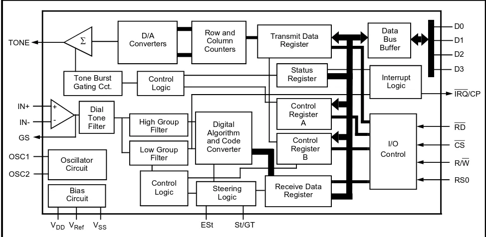
Row and Column Counters Transmit Data Register Data Bus Buffer Tone Burst Gating Cct. + -Oscillator Circuit Bias Circuit Control Logic Digital Algorithm and Code Converter Control Logic Steering Logic Status Register Control Register A Control Register B Receive Data Register Interrupt Logic I/O Control Low Group Filter High Group Filter Dial Tone Filter
ISSUE 2 May 1995
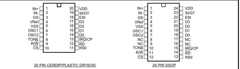
[image:30.595.70.557.510.748.2]Figure 2 - Pin Connections
Pin Description
Pin #
Name Description
20 24
1 1 IN+ Non-inverting op-amp input.
2 2 IN- Inverting op-amp input.
3 3 GS Gain Select. Gives access to output of front end differential amplifier for connection of feedback resistor.
4 4 VRef Reference Voltage output (VDD/2).
5 5 VSS Ground (0V).
6 6 OSC1 Oscillator input. This pin can also be driven directly by an external clock.
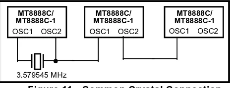
7 7 OSC2 Oscillator output. A 3.579545 MHz crystal connected between OSC1 and OSC2 completes the internal oscillator circuit. Leave open circuit when OSC1 is driven externally.
8 10 TONE Output from internal DTMF transmitter.
9 11 WR Write microprocessor input. TTL compatible.
10 12 CS Chip Select input. Active Low. This signal must be qualified externally by address latch enable (ALE) signal, see Figure 12.
11 13 RS0 Register Select input. Refer to Table 3 for bit interpretation. TTL compatible.
12 14 RD Read microprocessor input. TTL compatible.
13 15 IRQ/ CP
Interrupt Request/Call Progress (open drain) output. In interrupt mode, this output goes low when a valid DTMF tone burst has been transmitted or received. In call progress mode, this pin will output a rectangular signal representative of the input signal applied at the input op-amp. The input signal must be within the bandwidth limits of the call progress filter, see Figure 8.
14-17
18-21
D0-D3 Microprocessor Data Bus. High impedance when CS = 1 or RD = 1. TTL compatible.
18 22 ESt Early Steering output. Presents a logic high once the digital algorithm has detected a valid tone pair (signal condition). Any momentary loss of signal condition will cause ESt to return to a logic low.
19 23 St/GT Steering Input/Guard Time output (bidirectional). A voltage greater than VTSt detected at St causes the device to register the detected tone pair and update the output latch. A voltage less than VTSt frees the device to accept a new tone pair. The GT output acts to reset the external steering time-constant; its state is a function of ESt and the voltage on St.
20 24 VDD Positive power supply (5V typ.).
8,9 NC No Connection.
1 2 3 4 5 6 7 8 9 10 11 12 20 19 18 17 16 15 14 13 IN+ IN-GS VRef VSS OSC1 OSC2 TONE R/W CS VDD St/GT ESt D3 D2 D1 D0 IRQ/CP RD RS0 NC 1 2 3 4 5 6 7 8 9 10 11 12 13 14 15 16 24 23 22 21 20 19 18 17 IN+ IN-GS VRef VSS OSC1 OSC2 NC TONE R/W CS VDD St/GT ESt D3 D2 D1 D0 NC NC IRQ/CP RD RS0
The MT8888C/MT8888C-1 Integrated DTMF Transceiver consists of a high performance DTMF receiver with an internal gain setting amplifier and a DTMF generator which employs a burst counter to synthesize precise tone bursts and pauses. A call progress mode can be selected so that frequencies within the specified passband can be detected. The Intel micro interface allows microcontrollers, such as the 8080, 80C31/51 and 8085, to access the MT8888C/MT8888C-1 internal registers.
Input Configuration
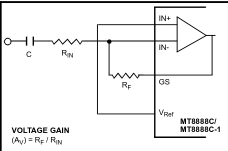
[image:32.595.326.558.94.394.2]The input arrangement of the MT8888C/MT8888C-1 provides a differential-input operational amplifier as well as a bias source (VRef), which is used to bias the inputs at VDD/2. Provision is made for connection of a feedback resistor to the op-amp output (GS) for gain adjustment. In a single-ended configuration, the input pins are connected as shown in Figure 3.
Figure 4 shows the necessary connections for a differential input configuration.
Receiver Section
Separation of the low and high group tones is achieved by applying the DTMF signal to the inputs of two sixth-order switched capacitor bandpass filters, the bandwidths of which correspond to the low and high group frequencies (see Table 1). These filters incorporate notches at 350 Hz and 440 Hz for exceptional dial tone rejection. Each filter output is followed by a single order switched capacitor filter section, which smooths the signals prior to limiting. Limiting is performed by high-gain comparators which are provided with hysteresis to prevent detection of unwanted low-level signals. The outputs of the comparators provide full rail logic swings at the frequencies of the incoming DTMF signals.
C RIN
RF IN+ IN-GS VRef VOLTAGE GAIN
(AV) = RF / RIN
[image:32.595.326.557.447.755.2]MT8888C/ MT8888C-1
Figure 4 - Differential Input Configuration
0= LOGIC LOW, 1= LOGIC HIGH
FLOW FHIGH DIGIT D3 D2 D1 D0
697 1209 1 0 0 0 1
697 1336 2 0 0 1 0
697 1477 3 0 0 1 1
770 1209 4 0 1 0 0
770 1336 5 0 1 0 1
770 1477 6 0 1 1 0
852 1209 7 0 1 1 1
852 1336 8 1 0 0 0
852 1477 9 1 0 0 1
941 1336 0 1 0 1 0
941 1209 * 1 0 1 1
941 1477 # 1 1 0 0
697 1633 A 1 1 0 1
770 1633 B 1 1 1 0
852 1633 C 1 1 1 1
941 1633 D 0 0 0 0
C1 C2 R1 R2 R3 R4 R5 IN+ IN-GS VRef MT8888C/
DIFFERENTIAL INPUT AMPLIFIER
C1 = C2 = 10 nF R1 = R4 = R5 = 100 kΩ
R2 = 60kΩ, R3 = 37.5 kΩ
R3 = (R2R5)/(R2 + R5)
VOLTAGE GAIN
(AV diff) - R5/R1
INPUT IMPEDANCE
(ZINdiff) = 2 R12 + (1/ωC)2
[image:32.595.72.300.605.756.2]digital counting techniques to determine the frequencies of the incoming tones and to verify that they correspond to standard DTMF frequencies. A complex averaging algorithm protects against tone simulation by extraneous signals such as voice while providing tolerance to small frequency deviations and variations. This averaging algorithm has been developed to ensure an optimum combination of immunity to talk-off and tolerance to the presence of interfering frequencies (third tones) and noise. When the detector recognizes the presence of two valid tones (this is referred to as the “signal condition” in some industry specifications) the “Early Steering” (ESt) output will go to an active state. Any subsequent loss of signal condition will cause ESt to assume an inactive state.
Steering Circuit
Before registration of a decoded tone pair, the receiver checks for a valid signal duration (referred to as character recognition condition). This check is performed by an external RC time constant driven by ESt. A logic high on ESt causes vc (see Figure 5) to rise as the capacitor discharges. Provided that the signal condition is maintained (ESt remains high) for the validation period (tGTP), vc reaches the threshold (VTSt) of the steering logic to register the tone pair, latching its corresponding 4-bit code (see Table 1) into the Receive Data Register. At this point the GT output is activated and drives vc to VDD. GT continues to drive high as long as ESt remains high. Finally, after a short delay to allow the output latch to settle, the delayed steering output flag goes high, signalling that a received tone pair has been registered. The status of the delayed steering flag can be monitored by checking the appropriate bit in the status register. If Interrupt mode has been selected, the IRQ/CP pin will pull low when the delayed steering flag is active.
[image:33.595.290.524.92.252.2]The contents of the output latch are updated on an active delayed steering transition. This data is presented to the four bit bidirectional data bus when the Receive Data Register is read. The steering circuit works in reverse to validate the interdigit pause between signals. Thus, as well as rejecting signals too short to be considered valid, the receiver will tolerate signal interruptions (drop out) too short to be considered a valid pause. This facility, together with the capability of selecting the steering time constants externally, allows the designer to tailor performance to meet a wide variety of system requirements.
Figure 5 - Basic Steering Circuit
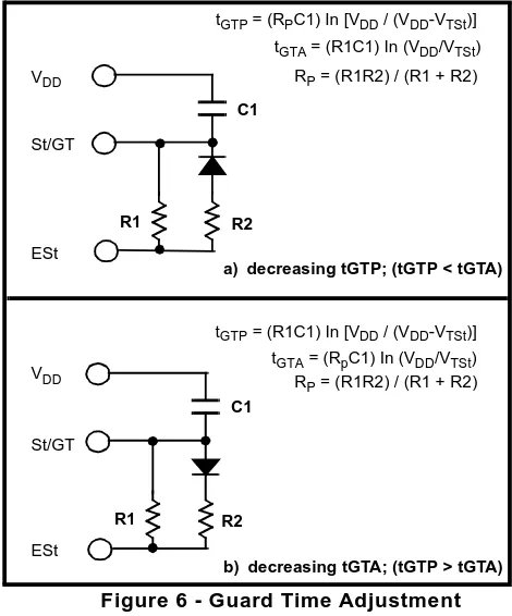
Guard Time Adjustment
The simple steering circuit shown in Figure 5 is adequate for most applications. Component values are chosen according to the following inequalities (see Figure 7):
tREC≥ tDPmax+tGTPmax - tDAmin tREC≤ tDPmin+tGTPmin - tDAmax tID≥ tDAmax+tGTAmax - tDPmin tDO≤ tDAmin+tGTAmin - tDPmax
The value of tDP is a device parameter (see AC Electrical Characteristics) and tREC is the minimum signal duration to be recognized by the receiver. A value for C1 of 0.1 µF is recommended for most
VDD VDD St/GT ESt C1 Vc R1 MT8888C/
tGTA = (R1C1) In (VDD / VTSt) tGTP = (R1C1) In [VDD / (VDD-VTSt)]
MT8888C-1 VDD St/GT ESt VDD St/GT ESt C1 R1 R2 C1 R1 R2
tGTA = (R1C1) In (VDD/VTSt)
tGTP = (RPC1) In [VDD / (VDD-VTSt)]
RP = (R1R2) / (R1 + R2)
tGTA = (RpC1) In (VDD/VTSt)
tGTP = (R1C1) In [VDD / (VDD-VTSt)]
RP = (R1R2) / (R1 + R2)
a) decreasing tGTP; (tGTP < tGTA)
[image:33.595.289.524.487.770.2]designer. Different steering arrangements may be used to select independent tone present (tGTP) and tone absent (tGTA) guard times. This may be necessary to meet system specifications which place both accept and reject limits on tone duration and interdigital pause. Guard time adjustment also allows the designer to tailor system parameters such as talk off and noise immunity.
Increasing tREC improves talk-off performance since it reduces the probability that tones simulated by speech will maintain a valid signal condition long enough to be registered. Alternatively, a relatively short tREC with a long tDO would be appropriate for extremely noisy environments where fast acquisition time and immunity to tone drop-outs are required. Design information for guard time adjustment is shown in Figure 6. The receiver timing is shown in Figure 7 with a description of the events in Figure 9.
Call Progress Filter
A call progress mode, using the MT8888C/ MT8888C-1, can be selected allowing the detection of various tones, which identify the progress of a telephone call on the network. The call progress tone input and DTMF input are common, however, call progress tones can only be detected when CP
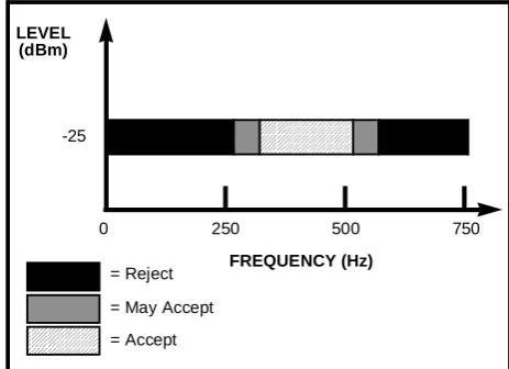
[image:34.595.324.556.244.412.2]detected if CP mode has been selected (see Table 7). Figure 8 indicates the useful detect bandwidth of the call progress filter. Frequencies presented to the input, which are within the ‘accept’ bandwidth limits of the filter, are hard-limited by a high gain comparator with the IRQ/CP pin serving as the output. The squarewave output obtained from the schmitt trigger can be analyzed by a microprocessor or counter arrangement to determine the nature of the call progress tone being detected. Frequencies which are in the ‘reject’ area will not be detected and consequently the IRQ/CP pin will remain low.
Figure 8 - Call Progress Response
LEVEL (dBm)
FREQUENCY (Hz)
-25
0 250 500 750
= Reject
= May Accept
= Accept
Vin
ESt
St/GT
RX0-RX3
b3
b2
Read Status Register
IRQ/CP
EVENTS A B C D E F
tREC tREC tID tDO
TONE #n TONE#n + 1 TONE#n + 1
tDP tDA
tGTP
tGTA
tPStRX
tPStb3
DECODED TONE # (n-1) # n # (n + 1)
[image:34.595.74.558.453.752.2]Figure 9 - Description of Timing Events
EXPLANATION OF EVENTS
A) TONE BURSTS DETECTED, TONE DURATION INVALID, RX DATA REGISTER NOT UPDATED.
B) TONE #n DETECTED, TONE DURATION VALID, TONE DECODED AND LATCHED IN RX DATA REGISTER.
C) END OF TONE #n DETECTED, TONE ABSENT DURATION VALID, INFORMATION IN RX DATA REGISTER
RETAINED UNTIL NEXT VALID TONE PAIR.
D) TONE #n+1 DETECTED, TONE DURATION VALID, TONE DECODED AND LATCHED IN RX DATA REGISTER.
E) ACCEPTABLE DROPOUT OF TONE #n+1, TONE ABSENT DURATION INVALID, DATA REMAINS UNCHANGED.
F) END OF TONE #n+1 DETECTED, TONE ABSENT DURATION VALID, INFORMATION IN RX DATA REGISTER
RETAINED UNTIL NEXT VALID TONE PAIR.
EXPLANATION OF SYMBOLS
Vin DTMF COMPOSITE INPUT SIGNAL.
ESt EARLY STEERING OUTPUT. INDICATES DETECTION OF VALID TONE FREQUENCIES.
St/GT STEERING INPUT/GUARD TIME OUTPUT. DRIVES EXTERNAL RC TIMING CIRCUIT.
RX0-RX3 4-BIT DECODED DATA IN RECEIVE DATA REGISTER
b3 DELAYED STEERING. INDICATES THAT VALID FREQUENCIES HAVE BEEN PRESENT/ABSENT FOR THE
REQUIRED GUARD TIME THUS CONSTITUTING A VALID SIGNAL. ACTIVE LOW FOR THE DURATION OF A VALID DTMF SIGNAL.
b2 INDICATES THAT VALID DATA IS IN THE RECEIVE DATA REGISTER. THE BIT IS CLEARED AFTER THE STATUS
REGISTER IS READ.
IRQ/CP INTERRUPT IS ACTIVE INDICATING THAT NEW DATA IS IN THE RX DATA REGISTER. THE INTERRUPT IS
CLEARED AFTER THE STATUS REGISTER IS READ.
tREC MAXIMUM DTMF SIGNAL DURATION NOT DETECTED AS VALID.
tREC MINIMUM DTMF SIGNAL DURATION REQUIRED FOR VALID RECOGNITION.
tID MINIMUM TIME BETWEEN VALID SEQUENTIAL DTMF SIGNALS.
tDO MAXIMUM ALLOWABLE DROPOUT DURING VALID DTMF SIGNAL.
tDP TIME TO DETECT VALID FREQUENCIES PRESENT.
tDA TIME TO DETECT VALID FREQUENCIES ABSENT.
tGTP GUARD TIME, TONE PRESENT.
tGTA GUARD TIME, TONE ABSENT.
DTMF Generator
The DTMF transmitter employed in the MT8888C/ MT8888C-1 is capable of generating all sixteen standard DTMF tone pairs with low distortion and high accuracy. All frequencies are derived from an external 3.579545 MHz crystal. The sinusoidal waveforms for the individual tones are digitally synthesized using row and column programmable dividers and switched capacitor D/A converters. The row and column tones are mixed and filtered providing a DTMF signal with low total harmonic distortion and high accuracy. To specify a DTMF signal, data conforming to the encoding format shown in Table 1 must be written to the transmit Data Register. Note that this is the same as the receiver output code. The individual tones which are generated (fLOW and fHIGH) are referred to as Low Group and High Group tones. As seen from the table, the low group frequencies are 697, 770, 852 and 941 Hz. The high group frequencies are 1209, 1336, 1477 and 1633 Hz. Typically, the high group to low group amplitude ratio (twist) is 2 dB to com-pensate for high group attenuation on long loops.
The period of each tone consists of 32 equal time segments. The period of a tone is controlled by
write operations to the Transmit Data Register the 4 bit data on the bus is latched and converted to 2 of 8 coding for use by the programmable divider circuitry. This code is used to specify a time segment length, which will ultimately determine the frequency of the tone. When the divider reaches the appropriate count, as determined by the input code, a reset pulse is issued and the counter starts again. The number of time segments is fixed at 32, however, by varying the segment length as described above the frequency can also be varied. The divider output clocks another counter, which addresses the sinewave lookup ROM.
Figure 10 - Spectrum Plot
Scaling Information
10 dB/Div
Start Frequency = 0 Hz Stop Frequency = 3400 Hz Marker Frequency = 697 Hz and 1209 Hz
Burst Mode
In certain telephony applications it is required that DTMF signals being generated are of a specific duration determined either by the particular application or by any one of the exchange transmitter specifications currently existing. Standard DTMF signal timing can be accomplished by making use of the Burst Mode. The transmitter is capable of issuing symmetric bursts/pauses of predetermined duration. This burst/pause duration is 51 ms±1 ms, which is a standard interval for autodialer and central office applications. After the burst/pause has been issued, the appropriate bit is set in the Status Register indicating that the transmitter is ready for more data. The timing described above is available when DTMF mode has been selected. However, when CP mode (Call Progress mode) is selected, the burst/pause duration is doubled to 102 ms ±2 ms. Note that when CP mode and Burst mode have been selected, DTMF tones may be transmitted only and not received. In applications where a non-standard burst/pause time is desirable, a software timing loop or external timer can be used to provide the timing pulses when the burst mode is disabled by enabling and disabling the transmitter.
Single Tone Generation
[image:36.595.328.557.688.753.2]A single tone mode is available whereby individual tones from the low group or high group can be generated. This mode can be used for DTMF test equipment applications, acknowledgment tone generation and distortion measurements. Refer to Control Register B description for details.
Table 2. Actual Frequencies Versus Standard Requirements
Distortion Calculations
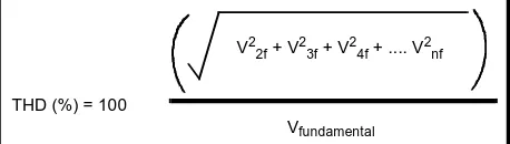
The MT8888C/MT8888C-1 is capable of producing precise tone bursts with minimal error in frequency (see Table 2). The internal summing amplifier is followed by a first-order lowpass switched capacitor filter to minimize harmonic components and intermodulation products. The total harmonic distortion for a single tone can be calculated using Equation 1, which is the ratio of the total power of all the extraneous frequencies to the power of the fundamental frequency expressed as a percentage.
ACTIVE INPUT
OUTPUT FREQUENCY (Hz)
%ERROR SPECIFIED ACTUAL
L1 697 699.1 +0.30
L2 770 766.2 -0.49
L3 852 847.4 -0.54
L4 941 948.0 +0.74
H1 1209 1215.9 +0.57
H2 1336 1331.7 -0.32
H3 1477 1471.9 -0.35
H4 1633 1645.0 +0.73
THD (%) = 100
Vfundamental