Intelligence is the faculty of making artificial objects, especially tools to make tools. —Henry Bergson (1859–1941)
A Hardware Description Language (HDL) is a formalism for defining and testing chips: objects whose interfaces consist of input and output pins that carry Boolean signals, and whose bodies are composed of interconnected collections of other, lower-level, chips. This appendix describes a typical HDL, as understood by the hardware simulator supplied with the book. Chapter 1 (in particular, section 1.1) provides essential background without which this appendix does not make much sense.
How to Use This Appendix This is a technical reference, and thus there is no need to read it from beginning to end. Instead, we recommended focusing on selected sections, as needed. Also, HDL is an intuitive and self-explanatory language, and the best way to learn it is to play with some HDL programs using the supplied hardware simulator. Therefore, we recommend to start experimenting with HDL programs as soon as you can, beginning with the following example.
A.1
Example
▸ Baca selengkapnya: elements of story structure
(2)though, the designer need not worry abouthowthese chips are implemented. When building a new chip in HDL, the internal parts that participate in the design are always viewed as black boxes, allowing the designer to focus only on their proper arrangement in the current chip architecture.
Thanks to this modularity, all HDL programs, including those that describe high-level chips, can be kept short and readable. For example, a complex chip like RAM16K can be implemented using a few internal parts (e.g., RAM4K chips), each described in a single HDL line. When fully evaluated by the hardware simulator all the way down the recursive chip hierarchy, these internal parts are expanded into many thousands of interconnected elementary logic gates. Yet the chip designer need not be concerned by this complexity, and can focus instead only on the chip’s top-most architecture.
A.2
Conventions
File extension: Each chip is defined in a separate text file. A chip whose name is Xxx is defined in fileXxx.hdl.
Chip structure: A chip definition consists of a header and a body. The header specifies the chip interface, and the body itsimplementation. The header acts as the chip’s API, or public documentation. The body should not interest people who use the chip as an internal part in other chip definitions.
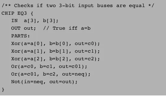
/** Checks if two 3-bit input buses are equal */ CHIP EQ3 {
IN a[3], b[3];
OUT out; // True iff a=b PARTS:
Xor(a=a[0], b=b[0], out=c0); Xor(a=a[1], b=b[1], out=c1); Xor(a=a[2], b=b[2], out=c2); Or(a=c0, b=c1, out=c01); Or(a=c01, b=c2, out=neq); Not(in=neq, out=out); }
Syntax conventions: HDL is case sensitive. HDL keywords are written in uppercase letters.
Identifier naming: Names of chips and pins may be any sequence of letters and digits not starting with a digit. By convention, chip and pin names start with a capi-tal letter and a lowercase letter, respectively. For readability, such names can include uppercase letters.
White space: Space characters, newline characters, and comments are ignored.
Comments: The following comment formats are supported:
// Comment to end of line /* Comment until closing */ /** API documentation comment */
A.3
Loading Chips into the Hardware Simulator
HDL programs (chip descriptions) are loaded into the hardware simulator in three different ways. First, the user can open an HDL file interactively, via a ‘‘load file’’ menu or GUI icon. Second, a test script (discussed here) can include aload Xxx.hdl command, which has the same effect. Finally, whenever an HDL program is loaded and parsed, every chip name Xxx listed in it as an internal part causes the simulator to load the respectiveXxx.hdlfile, all the way down the recursive chip hierarchy. In every one of these cases, the simulator goes through the following logic:
ifXxx.hdlexists in the current directory
then load it (and all its descendents) into the simulator else
ifXxx.hdlexists in the simulator’sbuiltInchips directory then load it (and all its descendents) into the simulator else
issue an error message.
simulator to use its built-in version instead, by simply moving the Xxx.hdlfile out from the current directory. Finally, in some cases the user (rather than the simulator) may want to load a built-in chip directly, for example, for experimentation. To do so, simply navigate to thetools/builtIndirectory—a standard part of the hard-ware simulator environment—and select the desired chip from there.
A.4
Chip Header (Interface)
The header of an HDL program has the following format:
CHIPchip name{
INinput pin name, input pin name, . . .; OUToutput pin name, output pin name, . . .; // Here comes the body.
}
m CHIP declaration: TheCHIPkeyword is followed by the chip name. The rest of the HDL code appears between curly brackets.
m Input pins: TheINkeyword is followed by a comma-separated list of input pin names. The list is terminated with a semicolon.
m Output pins: TheOUTkeyword is followed by a comma-separated list of output pin names. The list is terminated with a semicolon.
Input and output pins are assumed by default to be single-bit wide. A multi-bit bus can be declared using the notation pin name[w] (e.g.,a[3] in EQ3.hdl). This specifies that the pin is a bus of width w. The individual bits in a bus are indexed 0. . .w1, from right to left (i.e., index 0 refers to the least significant bit).
A.5
Chip Body (Implementation)
A.5.1 Parts
PARTS:
internal chip part; internal chip part; . . .
internal chip part;
Where each internal chip partstatement describes one internal chip with all its con-nections, using the syntax:
chip name(connection, . . . ,connection);
Where eachconnectionis described using the syntax:
part’s pin names¼chip’s pin name
(Throughout this appendix, the presently defined chip is calledchip, and the lower-level chips listed in thePARTSsection are calledparts).
A.5.2 Pins and Connections
Each connectiondescribes how one pin of a part is connected to another pin in the chip definition. In the simplest case, the programmer connects a part’s pin to an in-put or outin-put pin of the chip. In other cases, a part’s pin is connected to another pin of another part. This internal connection requires the introduction of aninternal pin, as follows:
Internal Pins In order to connect an output pin of one part to the input pins of other parts, the HDL programmer can create and use an internal pin, say v, as follows:
Part1 (..., out=v); // out of Part1 is piped into v Part2 (in=v, ...); // v is piped into in of Part2
Part3 (a=v, b=v, ...); // v is piped into both a and b of Part3
Input Pins Each input pin of a part may be fed by one of the following sources:
m an input pin of the chip
m an internal pin
m one of the constantstrueandfalse, representing 1 and 0, respectively
Each input pin has fan-in 1, meaning that it can be fed by one source only. Thus Part (in1=v,in2=v,...) is a valid statement, whereas Part (in1=v,in1=u, ...)is not.
Output Pins Each output pin of a part may feed one of the following destinations:
m an output pin of the chip
m an internal pin
A.5.3 Buses
Each pin used in a connection—whether input, output, or internal—may be a multi-bit bus. The widths (number of bits) of input and output pins are defined in the chip header. The widths of internal pins are deduced implicitly, from their connections.
In order to connect individual elements of a multi-bit bus input or output pin, the pin name (sayx) may be subscripted using the syntaxx[i]orx[i...j]=v, where v is an internal pin. This means that only the bits indexedito j(inclusive) of pinxare connected to the specified internal pin. An internal pin (like v above) may not be subscripted, and its width is deduced implicitly from the width of the bus pin to which it is connected the first time it is mentioned in the HDL program.
The constants true and false may also be used as buses, in which case the required width is deduced implicitly from the context of the connection.
Example
CHIP Foo {
IN in[8] // 8-bit input OUT out[8] // 8-bit output
// Foo's body (irrelevant to the example) }
Suppose now thatFoois invoked by another chip using the part statement:
wherevis a previously declared 3-bit internal pin, bound to some value. In that case, the connectionsin[2..4]=v andin[6..7]=truewill bind the inbus of the Foo chip to the following values:
7 6 5 4 3 2 1 0 (Bit)
in: 1 1 ? v[2] v[1] v[0] ? ? (Contents)
Now, let us assume that the logic of the Foo chip returns the following output:
7 6 5 4 3 2 1 0
out: 1 1 0 1 0 0 1 1
In that case, the connectionsout[0..3]=xandout[2..6]=ywill yield:
3 2 1 0 4 3 2 1 0
x: 0 0 1 1 y: 1 0 1 0 0
A.6
Built-In Chips
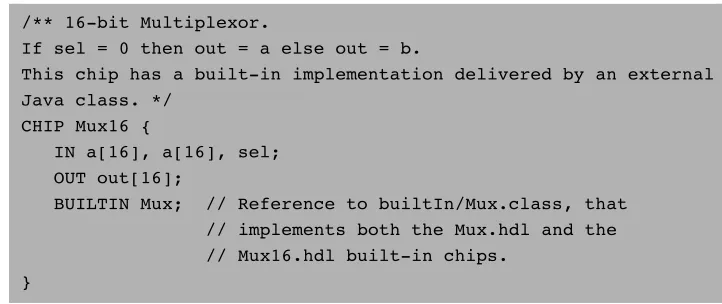
The hardware simulator features a library of built-in chips that can be used as inter-nal parts by other chips. Built-in chips are implemented in code written in a pro-gramming language like Java, operating behind an HDL interface. Thus, a built-in chip has a standard HDL header (interface), but its HDL body (implementation) declares it as built-in. Figure A.2 gives a typical example.
The identifier following the keyword BUILTIN is the name of the program unit that implements the chip logic. The present version of the hardware simulator is built in Java, and all the built-in chips are implemented as compiled Java classes. Hence, the HDL body of a built-in chip has the following format:
BUILTINJava class name;
where Java class nameis the name of the Java class that delivers the chip function-ality. Normally, this class will have the same name as that of the chip, for example Mux.class. All the built-in chips (compiled Java class files) are stored in a directory calledtools/builtIn, which is a standard part of the simulator’s environment.
Built-in chips provide three special services:
combinational and sequential chips, respectively. Thus the hardware simulator fea-tures built-in versions ofNand.hdlandDFF.hdl.
m Certification and efficiency: One way to modularize the development of a com-plex chip is to start by implementing built-in versions of its underlying chip parts. This enables the designer to build and test the chip logic while ignoring the logic of its lower-level parts—the simulator will automatically invoke their built-in imple-mentations. Additionally, it makes sense to use built-in versions even for chips that were already constructed in HDL, since the former are typically much faster and more space-efficient than the latter (simulation-wise). For example, when you load RAM4k.hdl into the simulator, the simulator creates a memory-resident data struc-ture consisting of thousands of lower-level chips, all the way down to the flip-flop gates at the bottom of the recursive chip hierarchy. Clearly, there is no need to repeat this drill-down simulation each timeRAM4Kis used as part in higher-level chips.Best practice tip:To boost performance and minimize errors, always use built-in versions of chips whenever they are available.
m Visualization: Some high-level chips (e.g., memory units) are easier to under-stand and debug if their operation can be inspected visually. To facilitate this ser-vice, built-in chips can be endowed (by their implementer) with GUI side effects. This GUI is displayed whenever the chip is loaded into the simulator or invoked as a lower-level part by the loaded chip. Except for these visual side effects, GUI-empowered chips behave, and can be used, just like any other chip. Section A.8 pro-vides more details about GUI-empowered chips.
/** 16-bit Multiplexor.
If sel = 0 then out = a else out = b.
This chip has a built-in implementation delivered by an external Java class. */
CHIP Mux16 {
IN a[16], a[16], sel; OUT out[16];
BUILTIN Mux; // Reference to builtIn/Mux.class, that // implements both the Mux.hdl and the // Mux16.hdl built-in chips.
}
A.7
Sequential Chips
Computer chips are eithercombinational orsequential(also calledclocked). The op-eration of combinational chips is instantaneous. When a user or a test script changes the values of one or more of the input pins of a combinational chip and reevaluates it, the simulator responds by immediately setting the chip output pins to a new set of values, as computed by the chip logic. In contrast, the operation of sequential chips is clock-regulated. When the inputs of a sequential chip change, the outputs of the chip may change only at the beginning of the next time unit, as effected by the simulated clock.
In fact, sequential chips (e.g., those implementing counters) may change their out-put values when the time changes even if none of their inout-puts changed. In contrast, combinational chips never change their values just because of the progression of time.
A.7.1 The Clock
The simulator models the progression of time by supporting two operations called tick andtock. These operations can be used to simulate a series oftime units, each consisting of two phases: a tickends the first phase of a time unit and starts its sec-ond phase, and atocksignals the first phase of the next time unit. Thereal timethat elapsed during this period is irrelevant for simulation purposes, since we have full control over the clock. In other words, either the simulator’s user or a test script can issue ticks andtocks at will, causing the clock to generate series of simulated time units.
The two-phased time units regulate the operations ofallthe sequential chip parts in the simulated chip architecture, as follows. During the first phase of the time unit (tick), the inputs of each sequential chip in the architecture are read and affect the chip’s internal state, according to the chip logic. During the second phase of the time unit (tock), the outputs of the chip are set to the new values. Hence, if we look at a sequential chip ‘‘from the outside,’’ we see that its output pins stabilize to new values only attocks—between consecutive time units.
repeat n {tick, tock, output;}. This particular example instructs the simulator to advance the clock n time units, and to print some values in the process. Test scripts and commands likerepeatandoutputare described in detail in appendix B.
A.7.2 Clocked Chips and Pins
A built-in chip can declare its dependence on the clock explicitly, using the statement:
CLOCKEDpin, pin, . . . ,pin;
where each pin is one of the input or output pins declared in the chip header. The inclusion of aninput pin xin theCLOCKEDlist instructs the simulator that changes to xshould not affect any of the chip’s output pins until the beginning of the next time unit. The inclusion of anoutput pin xin theCLOCKEDlist instructs the simulator that changes in any of the chip’s input pins should not affectxuntil the beginning of the next time unit.
Note that it is quite possible that only some of the input or output pins of a chip are declared as clocked. In that case, changes in the nonclocked input pins may affect the nonclocked output pins in a combinational manner, namely, independent of the clock. In fact, it is also possible to have the CLOCKEDkeyword with an empty list of pins, signifying that even though the chip may change its internal state depending on the clock, changes to any of its input pins may cause immediate changes to any of its output pins.
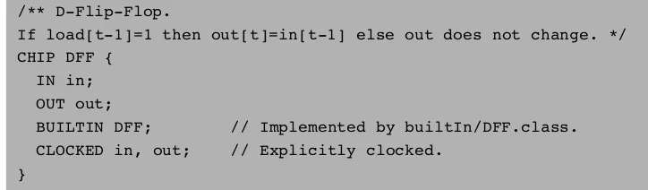
The ‘‘Clocked’’ Property of Chips How does the simulator know that a given chip is clocked? If the chip is built-in, then its HDL code may include the keyword CLOCKED. If the chip is not built-in, then it is said to be clocked when one or more of its lower-level chip parts are clocked. This ‘‘clocked’’ property is checked recursively, all the way down the chip hierarchy, where a built-in chip may be explicitly clocked. If such a chip is found, it renders every chip that depends on it (up the hierarchy) implicitly clocked. It follows that nothing in the HDL code of a given chip suggests that it may be clocked—the only way to know for sure is to read the chip documen-tation. For example, let us consider how the built-in DFF chip (figure A.3) impacts the ‘‘clockedness’’ of some of other chips presented in the book.
chips contains a DFF part. It follows that Bit, Register, RAM8, RAM64 and all the memory units above them are also clocked chips.
It’s important to remember that a sequential chip may well contain combinational logic that is not affected by the clock. For example, the structure of every sequen-tial RAM chip includes combinational circuits that manage its addressing logic (de-scribed in chapter 3).
A.7.3 Feedback Loops
We say that the use of a chip entails a feedback loop when the output of one of its parts affects the input of the same part, either directly or through some (possibly long) path of dependencies. For example, consider the following two examples of direct feedback dependencies:
Not (in=loop1, out=loop1) // Invalid DFF (in=loop2, out=loop2) // Valid
In each example, an internal pin (loop1orloop2) attempts to feed the chip’s input from its output, creating a cycle. The difference between the two examples is thatNot is acombinational chip whereas DFF isclocked. In the Not example,loop1creates an instantaneous and uncontrolled dependency between in and out, sometimes called data race. In the DFF case, the in-out dependency created by loop2 is delayed by the clocked logic of the DFF, and thusout(t)is not a function ofin(t) but rather ofin(t-1). In general, we have the following:
Valid/Invalid Feedback Loops When the simulator loads a chip, it checks recur-sively if its various connections entail feedback loops. For each loop, the simulator
/** D-Flip-Flop.
If load[t-1]=1 then out[t]=in[t-1] else out does not change. */ CHIP DFF {
IN in; OUT out;
BUILTIN DFF; // Implemented by builtIn/DFF.class. CLOCKED in, out; // Explicitly clocked.
}
checks if the loop goes through a clocked pin, somewhere along the loop. If so, the loop is allowed. Otherwise, the simulator stops processing and issues an error mes-sage. This is done in order to avoid uncontrolled data races.
A.8
Visualizing Chip Operations
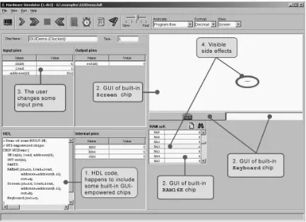
Built-in chips may be ‘‘GUI-empowered.’’ These chips feature visual side effects, designed to animate chip operations. A GUI-empowered chip can come to play in a simulation in two different ways, just like any other chip. First, the user can load it directly into the simulator. Second, and more typically, whenever a GUI-empowered chip is used as a part in the simulated chip, the simulator invokes it automatically. In both cases, the simulator displays the chip’s graphical image on the screen. Using this image, which is typically an interactive GUI component, one may inspect the current contents of the chip as well as change its internal state, when this operation is supported by the built-in chip implementation. The current version of this simulator features the following set of GUI-empowered chips:
ALU: Displays the Hack ALU’s inputs and output as well as the presently com-puted function.
Registers (There are three of them: ARegister—address register, DRegister—data register, and PC—program counter): Displays the contents of the register and allows modifying its contents.
Memory chips(ROM32K and various RAM chips): Displays a scrollable array-like image that shows the contents of all the memory locations and allows their modifi-cation. If the contents of a memory location changes during the simulation, the re-spective entry in the GUI changes as well. In the case of the ROM32K chip (which serves as the instruction memory of our computer platform), the GUI also features a button that enables loading a machine language program from an external text file. Screen chip: If the HDL code of a loaded chip invokes the built-in Screen chip, the hardware simulator displays a 256 rows by 512 columns window that simulates the physical screen. When the RAM-resident memory map of the screen changes during the simulation, the respective pixels in the screen GUI change as well, via a ‘‘refresh logic’’ embedded in the simulator implementation.
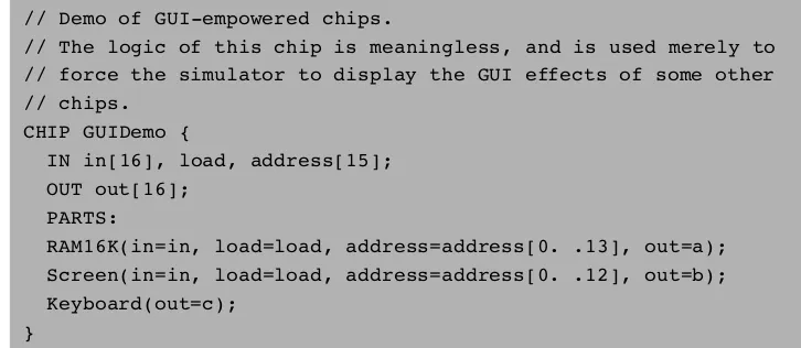
key pressed on the real keyboard is intercepted by the simulated chip, and its binary code is displayed in the keyboard’s RAM-resident memory map. If the user moves the mouse focus to another area in the simulator GUI, the control of the keyboard is restored to the real computer. Figure A.4 illustrates many of the features just described.
The chip logic in figure A.4 feeds the 16-bitinvalue into two destinations: register numberaddressin the RAM16K chip and register numberaddressin the Screen chip (presumably, the HDL programmer who wrote this code has figured out the widths of these address pins from the documentation of these chips). In addition, the chip logic routes the value of the currently pressed keyboard key to the internal pin c. These meaningless operations are designed for one purpose only: to illustrate how the simulator deals with built-in GUI-empowered chips. The actual impact is shown in figure A.5.
A.9
Supplied and New Built-In Chips
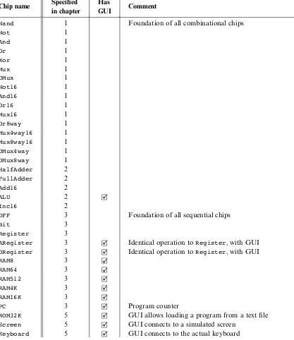
The built-in chips supplied with the hardware simulator are listed in figure A.6. These Java-based chip implementations were designed to support the construction and simulation of the Hack computer platform (although some of them can be used to support other 16-bit platforms). Users who wish to develop hardware platforms
// Demo of GUI-empowered chips.
// The logic of this chip is meaningless, and is used merely to // force the simulator to display the GUI effects of some other // chips.
CHIP GUIDemo {
IN in[16], load, address[15]; OUT out[16];
PARTS:
RAM16K(in=in, load=load, address=address[0. .13], out=a); Screen(in=in, load=load, address=address[0. .12], out=b); Keyboard(out=c);
}
Chip name Specified in chapter
Has
GUI Comment
Nand 1 Foundation of all combinational chips
Not 1
DFF 3 Foundation of all sequential chips
Bit 3
Register 3
ARegister 3 rZ Identical operation toRegister, with GUI
DRegister 3 rZ Identical operation toRegister, with GUI
RAM8 3 rZ
RAM64 3 rZ
RAM512 3 rZ
RAM4K 3 rZ
RAM16K 3 rZ
PC 3 rZ Program counter
ROM32K 5 rZ GUI allows loading a program from a text file
Screen 5 rZ GUI connects to a simulated screen
Keyboard 5 rZ GUI connects to the actual keyboard
other than Hack would probably benefit from the simulator’s ability to accommo-date new built-in chip definitions.