INTRODUCTION:
Frequency modulation, or FM, is an important method of impressing information on a carrier. It has
many advantages over AM. First, since FM only changes the frequency, and not the amplitude of the
carrier wave, FM receivers can be built to ignore amplitude (voltage) changes. This is important,
because most external noise is in the form of voltage variations that are "added" to the carrier wave as
it makes its way from transmitter to receiver. An AM receiver directly responds to these with the
familiar sounds of static interference; an FM receiver ignores the amplitude changes, almost
eliminating the effect of the noise.
Second, it is much easier to design systems to reproduce high-fidelity sound using FM. "High-fidelity"
means accurate signal reproduction, with a minimum of distortion. The reproduced information signal
is a very close replica of the original in an FM system. It's difficult to build hi-fi AM receivers, partly
due to the inherent nonlinear distortion created in a conventional AM diode detector, and also partly
due to the limited transmission bandwidth (8 kHz) allotted for AM broadcast.
These advantages do come at a price; that price is increased bandwidth. A typical FM broadcast station
uses up to 75 kHz of signal deviation (the peak frequency change), which results in a typical bandwidth
of 150 to 200 kHz. Because of the high bandwidth requirements, FM broadcasting is done in the VHF
band between 88 and 108 MHz. FM receivers and detectors are slightly more complex than those for
AM; and the higher frequencies used for FM (VHF) complicate overall transmitter and receiver design.
The circuitry in this lab operates on a carrier frequency of 100 kHz, which is in the VLF band. At such
a low carrier frequency, the frequency deviation needs to be limited so that the available bandwidth is
not used up. FM systems with limited deviation are very commonly used where the highest fidelity is
not needed. Voice-only communication systems in the amateur, business, and government radio
services are typical "narrowband" FM applications. Most narrowband FM communications occurs in the
VHF and UHF bands, where the reduced bandwidth requirement allows more stations to share the
available range of radio frequencies.
CIRCUIT ANALYSIS:
This experiment is in two parts, an FM modulator and an FM detector. The circuitry is designed to
operate in the VLF band at a carrier frequency of 100 kHz. The voltage-controlled-oscillator (VCO)
section of an LM565 PLL is used to create the FM waveform, and a second LM565 phase-locked-loop
(PLL) operates as the FM detector.
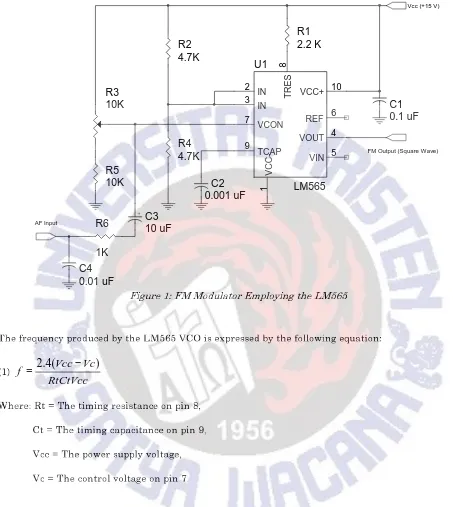
FM Modulator
C1
0.1 uF
R2
4.7K
R4
4.7K
R3
10K
R1
2.2 K
C2
0.001 uF
U1
LM565
IN 2 IN 3 VIN 5 TRES 8 TCAP 9 VCC-1 VCC+ 10 VCON 7 VOUT 4 REF 6R5
10K
C4
0.01 uF
R6
1K
C3
10 uF
+FM Output (Square W ave)
AF Input
Figure 1: FM Modulator Employing the LM565
The frequency produced by the LM565 VCO is expressed by the following equation:
(1)
RtCtVcc
Vc
Vcc
f
=
2
.
4
(
−
)
Where: Rt = The timing resistance on pin 8,
Ct = The timing capacitance on pin 9,
Vcc = The power supply voltage,
Vc = The control voltage on pin 7.
t
LM565 Pin 7 Voltage Vaverage AC Information SignalNotice that the audio signal is now riding on top of a DC level. Potentiometer R3 sets this DC level,
which controls the carrier center frequency. As the DC voltage rises, the VCO frequency decreases
in direct proportion to the amount of rise. The voltage "rise" is actually the same thing as the
amplitude of the information. Thus, positive information causes negative carrier frequency change or
deviation. The opposite effect happens on the negative peak of the intelligence; when the control
voltage falls, the VCO frequency increases. In other words, frequency modulation occurs.
Considerable amounts of RF signal from the VCO may “leak” out of pin 7 of the LM565. Components
R6 and C4 form a low-pass filter to prevent this RF energy from passing back to the audio input.
Modulator Sensitivity
The amount of frequency deviation produced in the VCO is directly proportional to the amplitude of the
information signal. The amount of deviation can be predicted by using the following equation:
(2)
δ
=
VmK
0Where: K
0is the modulator sensitivity, in Hz/Volt.
Vm = the peak information signal amplitude.
δ
= the deviation or peak frequency swing.
For example, if Vm=1/2 volt peak, and K
0= 50 kHz / Volt, then the amount of deviation produced will
be:
KHz
V
KHz
V
VmK
0=
(
0
.
5
)(
50
/
)
=
25
=
δ
The constant of the modulator in the experiment can be easily derived by differentiating equation (1)
with respect to Vc (recall that the control voltage Vc is the sum of the information signal, Vm(t) and
the average DC control voltage):
(3)
RtCtVcc
dVc
dF
K
02
.
4
−
=
=
(Hz/V)
This derivative is negative, indicating that positive intelligence voltage decreases the oscillator
frequency.
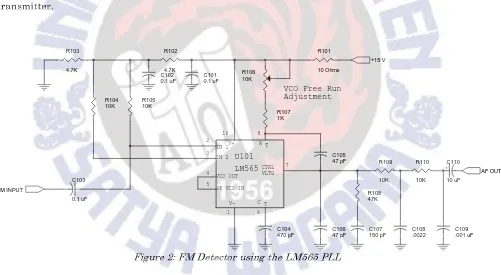
FM Detector:
Figure 2 shows the FM detector. It's based on the NE565 phase-locked-loop. The loop is set to free-run
at 100 kHz by C104 and the series combination of R107 and R106. Pot R106 allows adjustment of the
free-running frequency, which should be the same as the carrier or center frequency of the FM
transmitter.
V+ RT IN 1
IN 2
VCO OUT
PD VCO IN
V- C T 2 3 4 5 10 8 7 1 9 CTRL VLTG LM565
VCO Free Run Adjustment U101 R101 10 Ohms R106 10K R107 1K R109 10K R110 10K R108 47K C101 0.1 uF C102 0.1 uF C103 0.1 uF C104 470 pF C105 47 pF C106
47 pF C107150 pF C108.0022 C109.001 uF C110 10 uF + R102 4.7K R103 4.7K R104
10K R10510K
+15 V
FM INPUT
AF OUT
Figure 2: FM Detector using the LM565 PLL
corresponding to the "average" frequency going into the PLL from the FM modulator, and the other is
an AC level that is actually the detected information signal. This AC signal arises because of the PLL's
self-correcting action; as the transmitter deviates up or down in frequency, the PLL attempts to force
the VCO to follow this frequency
exactly
by varying its control voltage. Thus, the control voltage is a
copy of the original information signal.
LABORATORY PROCEDURE:
In this experiment you'll have two circuits to build. It is suggested that they be built on separate
breadboards, if possible.
1. Build the circuit of Figure 1. Don't connect anything to the AF INPUT yet.
2. Connect a frequency counter and scope to the FM OUTPUT of the circuit, and adjust R3 until a 100
kHz carrier wave is obtained. The waveshape from the VCO circuit will be a square wave.
3. Calculate K
0, the modulator sensitivity, by using equation (3).
4. Now connect a signal generator to the AF INPUT. Adjust it for 5 kHz frequency, and correct peak
voltage for 10 kHz deviation. (Use the result from step 3).
5. Connect scope channel 1 to the AF INPUT, and scope channel 2 to the FM OUTPUT. Trigger off
scope channel 1. Adjust the controls appropriately. Record the oscilloscope graph: FM Output vs AF
INPUT. Can you see the frequency deviation taking place? Why or why not?
6. Using the Agilent 54622D’s spectrum analyzer feature, look at the spectrum being displayed on
channel 1. Record this spectrum. Calculate the theoretical spectrum and compare the results.
7. Build the circuit of Figure 2. Keep component lead lengths as short as possible.
8. Apply power to the demodulator circuit, but don't connect its FM INPUT to anything yet. First,
adjust R106 so that the free-running VCO output on pin 4 of the NE565 PLL is 100 kHz. Use a
frequency counter for this measurement (the frequency counter function of the digital scope is
sufficiently accurate for this adjustment.)
Important: You must use proper RF grounding techniques for this experiment to work properly.
Use only one bus for ground, and keep all wires and leads as short as possible.
TIP: To get the best picture of the FM signal on the ‘54622D, the following settings are
suggested:
Timebase: 100
µ
S/div (or 2 MSample/s)
Center Frequency: 100 kHz
Span: 100 kHz
Window: HANNING
grounds! Connect the scope probes as follows: Channel 1 to the AF INPUT of the FM modulator,
and Channel 2 to the AF OUT of the FM detector. Record the oscilloscope graph: Detected FM
Output vs AF Input.
Note: Make sure the amplitude and frequency of the function generator are set correctly as in step 4.
10. How accurate is the reproduction of the information at the detector, when compared to the original
information (scope channel 1)? Use the subtract feature of the oscilloscope to find out. Set up an
oscilloscope trace that is the difference of channels 1 and 2 (use the math menu). You may need to
scale the channels appropriately to get “null” on equal signals. A system that isn’t creating any
distortion will have an input-output difference signal of zero.
11. Increase the deviation at the modulator (by adjusting the amplitude of the signal generator) until
the detected output just begins to become distorted.
1. What characteristic of the carrier is varied during Frequency Modulation?
______________________________________________________________________
______________________________________________________________________
2. What controls the amount of deviation in an FM transmitter?
______________________________________________________________________
______________________________________________________________________
3. What did R3 adjust? Why was this important?
______________________________________________________________________
______________________________________________________________________
______________________________________________________________________
4. What causes the voltage at pin 7 of the FM demodulator (NE565) to follow the original information
signal?
______________________________________________________________________
______________________________________________________________________
LM139/LM239/LM339/LM2901/LM3302 Low Power Low Offset Voltage Quad Comparators
Check for Samples:LM139-N,LM239-N,LM2901-N,LM3302-N,LM339-N
1
FEATURES
APPLICATIONS
2
•
Wide Supply Voltage Range
•
Limit Comparators
•
LM139/139A Series 2 to 36 V
DCor ±1 to ±18 V
DC•
Simple Analog-to-Digital Converters
•
LM2901: 2 to 36 V
DCor ±1 to ±18 V
DC•
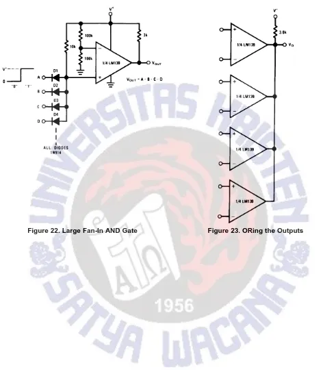
Pulse, Squarewave and Time Delay Generators
•
LM3302: 2 to 28 V
DCor ±1 to ±14 V
DC•
Wide Range VCO; MOS Clock Timers
•
Very Low Supply Current Drain (0.8 mA) —
•
Multivibrators and High Voltage Digital Logic
Independent of Supply Voltage
Gates
•
Low Input Biasing Current: 25 nA
DESCRIPTION
•
Low Input Offset Current: ±5 nA
The LM139 series consists of four independent
•
Offset Voltage: ±3 mV
precision voltage comparators with an offset voltage
•
Input Common-Mode Voltage Range Includes
specification as low as 2 mV max for all four
GND
comparators. These were designed specifically to
operate from a single power supply over a wide range
•
Differential Input Voltage Range Equal to the
of voltages. Operation from split power supplies is
Power Supply Voltage
also possible and the low power supply current drain
•
Low Output Saturation Voltage: 250 mV at 4
is independent of the magnitude of the power supply
mA
voltage. These comparators also have a unique
characteristic in that the input common-mode voltage
•
Output Voltage Compatible with TTL, DTL,
range includes ground, even though operated from a
ECL, MOS and CMOS Logic Systems
single power supply voltage.
ADVANTAGES
The LM139 series was designed to directly interface
with TTL and CMOS. When operated from both plus
•
High Precision Comparators
and minus power supplies, they will directly interface
•
Reduced V
OSDrift Over Temperature
with MOS logic— where the low power drain of the
•
Eliminates Need for Dual Supplies
LM339
is
a
distinct
advantage
over
standard
comparators.
•
Allows Sensing Near GND
•
Compatible with all Forms of Logic
One-Shot Multivibrator with Input Lock Out
Connection Diagrams
Figure 1. CDIP, SOIC, PDIP Packages – Top View
See Package Numbers J0014A, D0014A, NFF0014A
Figure 2. CLGA Package
Absolute Maximum Ratings
(1)LM139/LM239/LM339
LM139A/LM239A/LM339A LM3302
LM2901
Supply Voltage, V+ 36 VDCor ±18 VDC 28 VDCor ±14 VDC
Differential Input Voltage(2) 36 VDC 28 VDC
Input Voltage −0.3 VDCto +36 VDC −0.3 VDCto +28 VDC
Input Current (VIN<−0.3 VDC)(3) 50 mA 50 mA
Power Dissipation(4)
PDIP 1050 mW 1050 mW
Cavity DIP 1190 mW
SOIC Package 760 mW
Output Short-Circuit to GND(5) Continuous Continuous
Storage Temperature Range −65°C to +150°C −65°C to +150°C
Lead Temperature (Soldering, 10 seconds) 260°C 260°C
Operating Temperature Range −40°C to +85°C
LM339/LM339A 0°C to +70°C
LM239/LM239A −25°C to +85°C
LM2901 −40°C to +85°C
LM139/LM139A −55°C to +125°C
Soldering Information
PDIP Package Soldering (10 seconds) 260°C 260°C
SOIC Package
Vapor Phase (60 seconds) 215°C 215°C
Infrared (15 seconds) 220°C 220°C
ESD rating (1.5 kΩin series with 100 pF) 600V 600V
(1) Refer to RETS139AX for LM139A military specifications and to RETS139X for LM139 military specifications.
(2) Positive excursions of input voltage may exceed the power supply level. As long as the other voltage remains within the common-mode range, the comparator will provide a proper output state. The low input voltage state must not be less than−0.3 VDC(or 0.3 VDCbelow the magnitude of the negative power supply, if used) (at 25°C).
(3) This input current will only exist when the voltage at any of the input leads is driven negative. It is due to the collector-base junction of the input PNP transistors becoming forward biased and thereby acting as input diode clamps. In addition to this diode action, there is also lateral NPN parasitic transistor action on the IC chip. This transistor action can cause the output voltages of the comparators to go to the V+voltage level (or to ground for a large overdrive) for the time duration that an input is driven negative. This is not destructive and normal output states will re-establish when the input voltage, which was negative, again returns to a value greater than−0.3 VDC(at 25°C).
(4) For operating at high temperatures, the LM339/LM339A, LM2901, LM3302 must be derated based on a 125°C maximum junction temperature and a thermal resistance of 95°C/W which applies for the device soldered in a printed circuit board, operating in a still air ambient. The LM239 and LM139 must be derated based on a 150°C maximum junction temperature. The low bias dissipation and the “ON-OFF” characteristic of the outputs keeps the chip dissipation very small (PD≤100 mW), provided the output transistors are allowed to saturate.
Electrical Characteristics
(V+=5 V
DC, TA= 25°C, unless otherwise stated)
LM139A LM239A, LM339A LM139
Parameter Test Conditions Units
Min Typ Max Min Typ Max Min Typ Max
Input Offset Voltage See(1) 1.0 2.0 1.0 2.0 2.0 5.0 mV
DC Input Bias Current IIN(+)or IIN(−)with Output in 25 100 25 250 25 100 nADC
Linear Range(2), VCM=0V
Input Offset Current IIN(+)−IIN(−), VCM=0V 3.0 25 5.0 50 3.0 25 nADC Input Common-Mode V+=30 V
DC(LM3302, 0 V+−1.5 0 V+−1.5 0 V+−1.5 VDC Voltage Range V+= 28 V
DC)(3)
Supply Current RL=∞on all Comparators, 0.8 2.0 0.8 2.0 0.8 2.0 mADC
RL=∞, V+= 36V, 1.0 2.5 1.0 2.5 mADC
(LM3302, V+= 28 VDC)
Voltage Gain RL≥15 kΩ, V+= 15 VDC 50 200 50 200 50 200 V/mV VO= 1 VDCto 11 VDC
Large Signal VIN= TTL Logic Swing, VREF= 300 300 300 ns
Response Time
1.4 VDC, VRL= 5 VDC, RL= 5.1 kΩ
Response Time VRL= 5 VDC, RL= 5.1 kΩ(4) 1.3 1.3 1.3 μs
Output Sink Current VIN(−)= 1 VDC, VIN(+)= 0, 6.0 16 6.0 16 6.0 16 mADC VO≤1.5 VDC
Saturation Voltage VIN(−)= 1 VDC, VIN(+)= 0, 250 400 250 400 250 400 mVDC ISINK≤4 mA
Output Leakage VIN(+)= 1 VDC,VIN(−)= 0, 0.1 0.1 0.1 nADC
Current V
O= 5 VDC
(1) At output switch point, VO≃1.4 VDC, RS= 0Ωwith V+from 5 VDCto 30 VDC; and over the full input common-mode range (0 VDCto V+
−1.5 VDC), at 25°C. For LM3302, V+from 5 VDCto 28 VDC.
(2) The direction of the input current is out of the IC due to the PNP input stage. This current is essentially constant, independent of the state of the output so no loading change exists on the reference or input lines.
(3) The input common-mode voltage or either input signal voltage should not be allowed to go negative by more than 0.3V. The upper end of the common-mode voltage range is V+−1.5V at 25°C, but either or both inputs can go to +30 VDCwithout damage (25V for LM3302), independent of the magnitude of V+.
Electrical Characteristics
(V+= 5 V
DC, TA= 25°C, unless otherwise stated)
LM239, LM339 LM2901 LM3302
Parameter Test Conditions Units
Min Typ Max Min Typ Max Min Typ Max
Input Offset Voltage See(1) 2.0 5.0 2.0 7.0 3 20 mV
DC Input Bias Current IIN(+)or IIN(−)with Output in Linear 25 250 25 250 25 500 nADC
Range(2), V CM=0V
Input Offset Current IIN(+)−IIN(−), VCM= 0V 5.0 50 5 50 3 100 nADC Input Common-Mode V+= 30 VDC(LM3302, 0 V+−1.5 0 V+−1.5 0 V+−1.5 VDC
Voltage Range V+= 28 VDC)(3)
Supply Current RL=∞on all Comparators, 0.8 2.0 0.8 2.0 0.8 2.0 mADC
RL=∞, V+= 36V, 1.0 2.5 1.0 2.5 1.0 2.5 mADC
(LM3302, V+= 28 VDC)
Voltage Gain RL≥15 kΩ, V+= 15 VDC 50 200 25 100 2 30 V/mV VO= 1 VDCto 11 VDC
Large Signal VIN= TTL Logic Swing, VREF= 300 300 300 ns
Response Time 1.4 V
DC, VRL= 5 VDC, RL= 5.1 kΩ,
Response Time VRL= 5 VDC, RL= 5.1 kΩ(4) 1.3 1.3 1.3 μs
Output Sink Current VIN(−)= 1 VDC, VIN(+)= 0, 6.0 16 6.0 16 6.0 16 mADC VO≤1.5 VDC
Saturation Voltage VIN(−)= 1 VDC, VIN(+)= 0, 250 400 250 400 250 500 mVDC ISINK≤4 mA
Output Leakage VIN(+)= 1 VDC,VIN(−)= 0, 0.1 0.1 0.1 nADC Current
VO= 5 VDC
(1) At output switch point, VO≃1.4 VDC, RS= 0Ωwith V+from 5 VDCto 30 VDC; and over the full input common-mode range (0 VDCto V+
−1.5 VDC), at 25°C. For LM3302, V+from 5 VDCto 28 VDC.
(2) The direction of the input current is out of the IC due to the PNP input stage. This current is essentially constant, independent of the state of the output so no loading change exists on the reference or input lines.
(3) The input common-mode voltage or either input signal voltage should not be allowed to go negative by more than 0.3V. The upper end of the common-mode voltage range is V+−1.5V at 25°C, but either or both inputs can go to +30 VDCwithout damage (25V for LM3302), independent of the magnitude of V+.
Electrical Characteristics
(V+= 5.0 V DC(1))
LM139A LM239A, LM339A LM139
Parameter Test Conditions Units
Min Typ Max Min Typ Max Min Typ Max
Input Offset Voltage See(2) 4.0 4.0 9.0 mV
DC Input Offset Current IIN(+)−IIN(−), VCM= 0V 100 150 100 nADC Input Bias Current IIN(+)or IIN(−)with Output in 300 400 300 nADC
Linear Range, VCM= 0V(3) Input Common-Mode V+=30 V
DC(LM3302, 0 V+−2.0 0 V+−2.0 0 V+−2.0 VDC Voltage Range V+= 28 V
DC)(4)
Saturation Voltage VIN(−)=1 VDC, VIN(+)= 0, 700 700 700 mVDC ISINK≤4 mA
Output Leakage Current VIN(+) =1 VDC, VIN(−)= 0, 1.0 1.0 1.0 μADC VO= 30 VDC, (LM3302,
VO= 28 VDC)
Differential Input Voltage Keep all VIN's≥0 VDC(or V−, if 36 36 36 VDC used)(5)
(1) These specifications are limited to−55°C≤TA≤+125°C, for the LM139/LM139A. With the LM239/LM239A, all temperature
specifications are limited to−25°C≤TA≤+85°C, the LM339/LM339A temperature specifications are limited to 0°C≤TA≤+70°C, and the LM2901, LM3302 temperature range is−40°C≤TA≤+85°C.
(2) At output switch point, VO≃1.4 VDC, RS= 0Ωwith V+from 5 VDCto 30 VDC; and over the full input common-mode range (0 VDCto V+
−1.5 VDC), at 25°C. For LM3302, V+from 5 VDCto 28 VDC.
(3) The direction of the input current is out of the IC due to the PNP input stage. This current is essentially constant, independent of the state of the output so no loading change exists on the reference or input lines.
(4) The input common-mode voltage or either input signal voltage should not be allowed to go negative by more than 0.3V. The upper end of the common-mode voltage range is V+−1.5V at 25°C, but either or both inputs can go to +30 V
DCwithout damage (25V for LM3302), independent of the magnitude of V+.
Electrical Characteristics
(V+= 5.0 V DC(1))
LM239, LM339 LM2901 LM3302
Parameter Test Conditions Units
Min Typ Max Min Typ Max Min Typ Max
Input Offset Voltage See(2) 9.0 9 15 40 mV
DC Input Offset Current IIN(+)−IIN(−), VCM= 0V 150 50 200 300 nADC Input Bias Current IIN(+)or IIN(−)with Output in 400 200 500 1000 nADC
Linear Range, VCM= 0V(3) Input Common-Mode V+= 30 V
DC(LM3302, V+−2.0 0 V+−2.0 0 V+−2.0 VDC V+= 28 VDC)
Voltage Range See(4)
Saturation Voltage VIN(−)= 1 VDC, VIN(+)= 0, 700 400 700 700 mVDC ISINK≤4 mA
Output Leakage Current VIN(+) =1 VDC, VIN(−)= 0, VO= 30 1.0 1.0 1.0 μADC VDC, (LM3302, VO= 28 VDC)
Differential Input Voltage Keep all VIN's≥0 VDC(or V−, if 36 36 28 VDC used)(5)
(1) These specifications are limited to−55°C≤TA≤+125°C, for the LM139/LM139A. With the LM239/LM239A, all temperature
specifications are limited to−25°C≤TA≤+85°C, the LM339/LM339A temperature specifications are limited to 0°C≤TA≤+70°C, and the LM2901, LM3302 temperature range is−40°C≤TA≤+85°C.
(2) At output switch point, VO≃1.4 VDC, RS= 0Ωwith V+from 5 VDCto 30 VDC; and over the full input common-mode range (0 VDCto V+
−1.5 VDC), at 25°C. For LM3302, V+from 5 VDCto 28 VDC.
(3) The direction of the input current is out of the IC due to the PNP input stage. This current is essentially constant, independent of the state of the output so no loading change exists on the reference or input lines.
(4) The input common-mode voltage or either input signal voltage should not be allowed to go negative by more than 0.3V. The upper end of the common-mode voltage range is V+−1.5V at 25°C, but either or both inputs can go to +30 V
DCwithout damage (25V for LM3302), independent of the magnitude of V+.
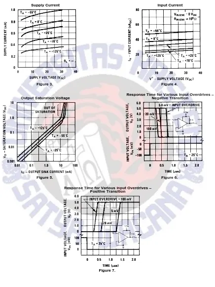
Typical Performance Characteristics
LM139/LM239/LM339, LM139A/LM239A/LM339A, LM3302
Supply Current Input Current
Figure 3. Figure 4.
Response Time for Various Input Overdrives –
Output Saturation Voltage Negative Transition
Figure 5. Figure 6.
Response Time for Various Input Overdrives – Positive Transition
Typical Performance Characteristics
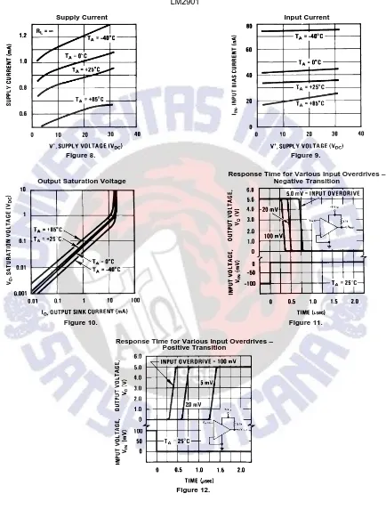
LM2901
Supply Current Input Current
Figure 8. Figure 9.
Response Time for Various Input Overdrives –
Output Saturation Voltage Negative Transition
Figure 10. Figure 11.
Response Time for Various Input Overdrives – Positive Transition
Application Hints
The LM139 series are high gain, wide bandwidth devices which, like most comparators, can easily oscillate if the
output lead is inadvertently allowed to capacitively couple to the inputs via stray capacitance. This shows up only
during the output voltage transition intervals as the comparator changes states. Power supply bypassing is not
required to solve this problem. Standard PC board layout is helpful as it reduces stray input-output coupling.
Reducing this input resistors to < 10 k
Ω
reduces the feedback signal levels and finally, adding even a small
amount (1 to 10 mV) of positive feedback (hysteresis) causes such a rapid transition that oscillations due to stray
feedback are not possible. Simply socketing the IC and attaching resistors to the pins will cause input-output
oscillations during the small transition intervals unless hysteresis is used. If the input signal is a pulse waveform,
with relatively fast rise and fall times, hysteresis is not required.
All pins of any unused comparators should be tied to the negative supply.
The bias network of the LM139 series establishes a drain current which is independent of the magnitude of the
power supply voltage over the range of from 2 V
DCto 30 V
DC.
It is usually unnecessary to use a bypass capacitor across the power supply line.
The differential input voltage may be larger than V
+without damaging the device. Protection should be provided
to prevent the input voltages from going negative more than
−
0.3 V
DC(at 25°C). An input clamp diode can be
used as shown in the applications section.
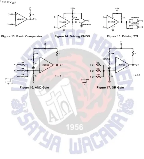
Typical Applications
(V
+= 5.0 V
DC)
Figure 13. Basic Comparator
Figure 14. Driving CMOS
Figure 15. Driving TTL
Typical Applications
(V
+= 15 V
DC)
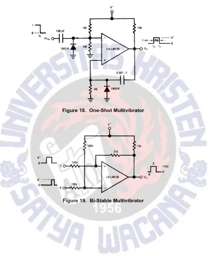
Figure 18. One-Shot Multivibrator
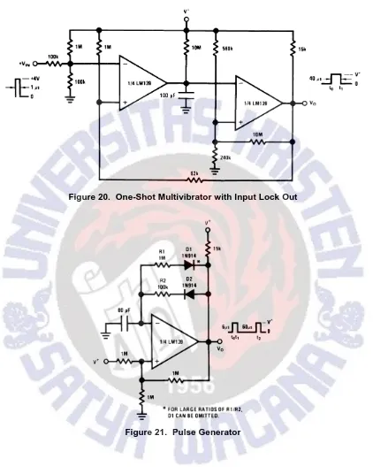
Figure 20. One-Shot Multivibrator with Input Lock Out
Figure 27. Squarewave Oscillator
Figure 28. Basic Comparator
* Or open-collector logic gate without pull-up resistor
Figure 31. Output Strobing
Figure 32. Crystal Controlled Oscillator
V+= +30 VDC
250 mVDC≤VC≤+50 VDC 700 Hz≤fO≤100 kHz
Split-Supply Applications
(V
+= +15 V
DCand V
−=
−
15 V
DC)
Figure 36. MOS Clock Driver
REVISION HISTORY
Changes from Revision C (March 2013) to Revision D Page
www.ti.com 12-Jul-2014
PACKAGING INFORMATION
Orderable Device Status
(1)
Package Type Package Drawing Pins Package Qty Eco Plan (2) Lead/Ball Finish (6)
MSL Peak Temp
(3)
Op Temp (°C) Device Marking
(4/5)
Samples
LM139AJ/PB ACTIVE CDIP J 14 25 TBD Call TI Call TI -55 to 125 LM139AJ
LM139J/PB ACTIVE CDIP J 14 25 TBD Call TI Call TI -55 to 125 LM139J
LM239J ACTIVE CDIP J 14 25 TBD Call TI Call TI -25 to 85 LM239J
LM2901M NRND SOIC D 14 55 TBD Call TI Call TI -40 to 85 LM2901M
LM2901M/NOPB ACTIVE SOIC D 14 55 Green (RoHS & no Sb/Br)
CU SN Level-1-260C-UNLIM -40 to 85 LM2901M
LM2901MX NRND SOIC D 14 2500 TBD Call TI Call TI -40 to 85 LM2901M
LM2901MX/NOPB ACTIVE SOIC D 14 2500 Green (RoHS & no Sb/Br)
CU SN Level-1-260C-UNLIM -40 to 85 LM2901M
LM2901N/NOPB ACTIVE PDIP NFF 14 25 Green (RoHS & no Sb/Br)
CU SN Level-1-NA-UNLIM -40 to 85 LM2901N
LM2901N/PB LIFEBUY PDIP NFF 14 25 TBD Call TI Call TI LM2901N
LM339AM NRND SOIC D 14 55 TBD Call TI Call TI -25 to 85 LM339AM
LM339AM/NOPB ACTIVE SOIC D 14 55 Green (RoHS & no Sb/Br)
CU SN Level-1-260C-UNLIM -25 to 85 LM339AM
LM339AMX NRND SOIC D 14 2500 TBD Call TI Call TI -25 to 85 LM339AM
LM339AMX/NOPB ACTIVE SOIC D 14 2500 Green (RoHS & no Sb/Br)
CU SN Level-1-260C-UNLIM -25 to 85 LM339AM
LM339AN/NOPB ACTIVE PDIP NFF 14 25 Green (RoHS & no Sb/Br)
CU SN Level-1-NA-UNLIM -25 to 85 LM339AN
LM339AN/PB LIFEBUY PDIP NFF 14 25 TBD Call TI Call TI LM339AN
LM339J ACTIVE CDIP J 14 25 TBD Call TI Call TI -25 to 85 LM339J
LM339M NRND SOIC D 14 55 TBD Call TI Call TI -25 to 85 LM339M
www.ti.com 12-Jul-2014
Orderable Device Status
(1)
Package Type Package Drawing Pins Package Qty Eco Plan (2) Lead/Ball Finish (6)
MSL Peak Temp
(3)
Op Temp (°C) Device Marking
(4/5)
Samples
LM339N/PB LIFEBUY PDIP NFF 14 25 TBD Call TI Call TI LM339N
MLM339P LIFEBUY PDIP NFF 14 25 TBD Call TI Call TI LM339N
(1)
The marketing status values are defined as follows:
ACTIVE: Product device recommended for new designs.
LIFEBUY: TI has announced that the device will be discontinued, and a lifetime-buy period is in effect.
NRND: Not recommended for new designs. Device is in production to support existing customers, but TI does not recommend using this part in a new design. PREVIEW: Device has been announced but is not in production. Samples may or may not be available.
OBSOLETE: TI has discontinued the production of the device.
(2)
Eco Plan - The planned eco-friendly classification: Pb-Free (RoHS), Pb-Free (RoHS Exempt), or Green (RoHS & no Sb/Br) - please check http://www.ti.com/productcontent for the latest availability information and additional product content details.
TBD: The Pb-Free/Green conversion plan has not been defined.
Pb-Free (RoHS): TI's terms "Lead-Free" or "Pb-Free" mean semiconductor products that are compatible with the current RoHS requirements for all 6 substances, including the requirement that
lead not exceed 0.1% by weight in homogeneous materials. Where designed to be soldered at high temperatures, TI Pb-Free products are suitable for use in specified lead-free processes.
Pb-Free (RoHS Exempt): This component has a RoHS exemption for either 1) lead-based flip-chip solder bumps used between the die and package, or 2) lead-based die adhesive used between
the die and leadframe. The component is otherwise considered Pb-Free (RoHS compatible) as defined above.
Green (RoHS & no Sb/Br): TI defines "Green" to mean Pb-Free (RoHS compatible), and free of Bromine (Br) and Antimony (Sb) based flame retardants (Br or Sb do not exceed 0.1% by weight
in homogeneous material)
(3)
MSL, Peak Temp. - The Moisture Sensitivity Level rating according to the JEDEC industry standard classifications, and peak solder temperature.
(4)
There may be additional marking, which relates to the logo, the lot trace code information, or the environmental category on the device.
(5)
Multiple Device Markings will be inside parentheses. Only one Device Marking contained in parentheses and separated by a "~" will appear on a device. If a line is indented then it is a continuation of the previous line and the two combined represent the entire Device Marking for that device.
(6)
Lead/Ball Finish - Orderable Devices may have multiple material finish options. Finish options are separated by a vertical ruled line. Lead/Ball Finish values may wrap to two lines if the finish value exceeds the maximum column width.
TAPE AND REEL INFORMATION
*All dimensions are nominal
Device Package Type
Package Drawing
Pins SPQ Reel Diameter (mm) Reel Width W1 (mm) A0 (mm) B0 (mm) K0 (mm) P1 (mm) W (mm) Pin1 Quadrant
LM2901MX SOIC D 14 2500 330.0 16.4 6.5 9.35 2.3 8.0 16.0 Q1 LM2901MX/NOPB SOIC D 14 2500 330.0 16.4 6.5 9.35 2.3 8.0 16.0 Q1 LM339AMX SOIC D 14 2500 330.0 16.4 6.5 9.35 2.3 8.0 16.0 Q1 LM339AMX/NOPB SOIC D 14 2500 330.0 16.4 6.5 9.35 2.3 8.0 16.0 Q1 LM339MX SOIC D 14 2500 330.0 16.4 6.5 9.35 2.3 8.0 16.0 Q1 LM339MX/NOPB SOIC D 14 2500 330.0 16.4 6.5 9.35 2.3 8.0 16.0 Q1
*All dimensions are nominal
Device Package Type Package Drawing Pins SPQ Length (mm) Width (mm) Height (mm)
LM2901MX SOIC D 14 2500 367.0 367.0 35.0
LM2901MX/NOPB SOIC D 14 2500 367.0 367.0 35.0
LM339AMX SOIC D 14 2500 367.0 367.0 35.0
LM339AMX/NOPB SOIC D 14 2500 367.0 367.0 35.0
LM339MX SOIC D 14 2500 367.0 367.0 35.0
LM339MX/NOPB SOIC D 14 2500 367.0 367.0 35.0
issue. Buyers should obtain the latest relevant information before placing orders and should verify that such information is current and complete. All semiconductor products (also referred to herein as “components”) are sold subject to TI’s terms and conditions of sale supplied at the time of order acknowledgment.
TI warrants performance of its components to the specifications applicable at the time of sale, in accordance with the warranty in TI’s terms and conditions of sale of semiconductor products. Testing and other quality control techniques are used to the extent TI deems necessary to support this warranty. Except where mandated by applicable law, testing of all parameters of each component is not necessarily performed.
TI assumes no liability for applications assistance or the design of Buyers’ products. Buyers are responsible for their products and applications using TI components. To minimize the risks associated with Buyers’ products and applications, Buyers should provide adequate design and operating safeguards.
TI does not warrant or represent that any license, either express or implied, is granted under any patent right, copyright, mask work right, or other intellectual property right relating to any combination, machine, or process in which TI components or services are used. Information published by TI regarding third-party products or services does not constitute a license to use such products or services or a warranty or endorsement thereof. Use of such information may require a license from a third party under the patents or other intellectual property of the third party, or a license from TI under the patents or other intellectual property of TI.
Reproduction of significant portions of TI information in TI data books or data sheets is permissible only if reproduction is without alteration and is accompanied by all associated warranties, conditions, limitations, and notices. TI is not responsible or liable for such altered documentation. Information of third parties may be subject to additional restrictions.
Resale of TI components or services with statements different from or beyond the parameters stated by TI for that component or service voids all express and any implied warranties for the associated TI component or service and is an unfair and deceptive business practice. TI is not responsible or liable for any such statements.
Buyer acknowledges and agrees that it is solely responsible for compliance with all legal, regulatory and safety-related requirements concerning its products, and any use of TI components in its applications, notwithstanding any applications-related information or support that may be provided by TI. Buyer represents and agrees that it has all the necessary expertise to create and implement safeguards which anticipate dangerous consequences of failures, monitor failures and their consequences, lessen the likelihood of failures that might cause harm and take appropriate remedial actions. Buyer will fully indemnify TI and its representatives against any damages arising out of the use of any TI components in safety-critical applications.
In some cases, TI components may be promoted specifically to facilitate safety-related applications. With such components, TI’s goal is to help enable customers to design and create their own end-product solutions that meet applicable functional safety standards and requirements. Nonetheless, such components are subject to these terms.
No TI components are authorized for use in FDA Class III (or similar life-critical medical equipment) unless authorized officers of the parties have executed a special agreement specifically governing such use.
Only those TI components which TI has specifically designated as military grade or “enhanced plastic” are designed and intended for use in military/aerospace applications or environments. Buyer acknowledges and agrees that any military or aerospace use of TI components which have not been so designated is solely at the Buyer's risk, and that Buyer is solely responsible for compliance with all legal and regulatory requirements in connection with such use.
TI has specifically designated certain components as meeting ISO/TS16949 requirements, mainly for automotive use. In any case of use of non-designated products, TI will not be responsible for any failure to meet ISO/TS16949.
Products Applications
Audio www.ti.com/audio Automotive and Transportation www.ti.com/automotive
Amplifiers amplifier.ti.com Communications and Telecom www.ti.com/communications
Data Converters dataconverter.ti.com Computers and Peripherals www.ti.com/computers
DLP® Products www.dlp.com Consumer Electronics www.ti.com/consumer-apps
DSP dsp.ti.com Energy and Lighting www.ti.com/energy
Clocks and Timers www.ti.com/clocks Industrial www.ti.com/industrial
Interface interface.ti.com Medical www.ti.com/medical
Logic logic.ti.com Security www.ti.com/security
Power Mgmt power.ti.com Space, Avionics and Defense www.ti.com/space-avionics-defense
Microcontrollers microcontroller.ti.com Video and Imaging www.ti.com/video
RFID www.ti-rfid.com
LM380 2.5W Audio Power Amplifier
Check for Samples:LM380
1
FEATURES
DESCRIPTION
The LM380 is a power audio amplifier for consumer
•
Wide Supply Voltage Range: 10V-22V
applications. In order to hold system cost to a
•
Low Quiescent Power Drain: 0.13W (V
S= 18V)
minimum, gain is internally fixed at 34 dB. A unique
•
Voltage Gain Fixed at 50
input stage allows ground referenced input signals.
The output automatically self-centers to one-half the
•
High Peak Current Capability: 1.3A
supply voltage.
•
Input Referenced to GND
The output is short circuit proof with internal thermal
•
High Input Impedance: 150k
Ω
limiting. The package outline is standard dual-in-line.
•
Low Distortion
The LM380N uses a copper lead frame. The center
•
Quiescent Output Voltage is at One-Half of the
three pins on either side comprise a heat sink. This
Supply Voltage
makes the device easy to use in standard PC layouts.
•
Standard Dual-In-Line Package
Uses
include
simple
phonograph
amplifiers,
intercoms, line drivers, teaching machine outputs,
alarms, ultrasonic drivers, TV sound systems, AM-FM
radio, small servo drivers, power converters, etc.
A selected part for more power on higher supply
voltages is available as the LM384. For more
information see
SNAA086
.
Connection Diagrams
[image:38.612.53.558.136.600.2](Dual-In-Line Packages, Top View)
Figure 1. 14-Pin PDIP
Figure 2. 8-Pin PDIP
Block and Schematic Diagrams
Figure 3. 14-Pin PDIP
Figure 4. 8-Pin PDIP
These devices have limited built-in ESD protection. The leads should be shorted together or the device placed in conductive foam during storage or handling to prevent electrostatic damage to the MOS gates.
Absolute Maximum Ratings
(1) (2)Supply Voltage 22V
Peak Current 1.3A
Package Dissipation 14-Pin PDIP(3) 8.3W
8-Pin PDIP(3) 1.67W
Input Voltage ±0.5V
Storage Temperature −65°C to +150°C
Operating Temperature 0°C to +70°C
Junction Temperature +150°C
Lead Temperature (Soldering, 10 sec.) +260°C
ESD rating to be determined
Thermal Resistance θJC(14-Pin PDIP) 30°C/W
θJC(8-Pin PDIP) 37°C/W
θJA(14-Pin PDIP) 79°C/W
θJA(8-Pin PDIP) 107°C/W
(1) "Absolute Maximum Ratings" indicate limits beyond which damage to the device may occur. Operating Ratings indicate conditions for which the device is functional, but do not ensure specific performance limits.
(2) If Military/Aerospace specified devices are required, please contact the Texas Instruments Sales Office/Distributors for availability and specifications.
(3) The package is to be derated at 15°C/W junction to heat sink pins for 14-pin pkg; 75°C/W for 8-pin.
Electrical Characteristics
(1)Symbol Parameter Conditions Min Typ Max Units
POUT(RMS) Output Power RL= 8Ω, THD = 3%(2) (3) 2.5 W
AV Gain 40 50 60 V/V
VOUT Output Voltage Swing RL= 8Ω 14 Vp-p
ZIN Input Resistance 150k Ω
THD Total Harmonic Distortion See(3) (4) 0.2 %
PSRR Power Supply Rejection Ratio See(5) 38 dB
VS Supply Voltage 10 22 V
BW Bandwidth POUT= 2W, RL= 8Ω 100k Hz
IQ Quiescent Supply Current 7 25 mA
VOUTQ Quiescent Output Voltage 8 9.0 10 V
IBIAS Bias Current Inputs Floating 100 nA
ISC Short Circuit Current 1.3 A
(1) VS= 18V and TA= 25°C unless otherwise specified.
(2) With device Pins 3, 4, 5, 10, 11, 12 soldered into a 1/16″epoxy glass board with 2 ounce copper foil with a minimum surface of 6 square inches.
(3) CBYPASS= 0.47μfd on Pin 1.
Heat Sink Dimensions
Typical Performance Characteristics
[image:42.612.84.538.81.690.2]Maximum Device Dissipation vs Ambient Temperature Device Dissipation vs Output Power—4ΩLoad
Figure 6. Figure 7.
Device Dissipation vs Output Power—8ΩLoad Device Dissipation vsOutput Power—16ΩLoad
Figure 8. Figure 9.
Typical Performance Characteristics (continued)
[image:43.612.77.529.71.633.2]Output Voltage Gain and Phase vs Frequency Total Harmonic Distortion vs Output Power
Figure 12. Figure 13.
Device Dissipation vs Output Power Supply Decoupling vs Frequency
Typical Applications
Figure 16. Phono Amplifier
Figure 17. Bridge Amplifier
REVISION HISTORY
Changes from Revision B (April 2013) to Revision C Page
www.ti.com 27-Mar-2014
PACKAGING INFORMATION
Orderable Device Status
(1)
Package Type Package Drawing Pins Package Qty Eco Plan (2) Lead/Ball Finish (6)
MSL Peak Temp
(3)
Op Temp (°C) Device Marking
(4/5)
Samples
LM380N LIFEBUY PDIP NFF 14 25 TBD Call TI Call TI 0 to 70 LM380N
LM380N-8/NOPB ACTIVE PDIP P 8 40 Green (RoHS & no Sb/Br)
CU SN Level-1-NA-UNLIM 0 to 70 LM 380N-8 LM380N/NOPB ACTIVE PDIP NFF 14 25 Pb-Free (RoHS
Exempt)
CU SN Level-1-NA-UNLIM 0 to 70 LM380N
(1)
The marketing status values are defined as follows:
ACTIVE: Product device recommended for new designs.
LIFEBUY: TI has announced that the device will be discontinued, and a lifetime-buy period is in effect.
NRND: Not recommended for new designs. Device is in production to support existing customers, but TI does not recommend using this part in a new design. PREVIEW: Device has been announced but is not in production. Samples may or may not be available.
OBSOLETE: TI has discontinued the production of the device.
(2)
Eco Plan - The planned eco-friendly classification: Pb-Free (RoHS), Pb-Free (RoHS Exempt), or Green (RoHS & no Sb/Br) - please check http://www.ti.com/productcontent for the latest availability information and additional product content details.
TBD: The Pb-Free/Green conversion plan has not been defined.
Pb-Free (RoHS): TI's terms "Lead-Free" or "Pb-Free" mean semiconductor products that are compatible with the current RoHS requirements for all 6 substances, including the requirement that
lead not exceed 0.1% by weight in homogeneous materials. Where designed to be soldered at high temperatures, TI Pb-Free products are suitable for use in specified lead-free processes.
Pb-Free (RoHS Exempt): This component has a RoHS exemption for either 1) lead-based flip-chip solder bumps used between the die and package, or 2) lead-based die adhesive used between
the die and leadframe. The component is otherwise considered Pb-Free (RoHS compatible) as defined above.
Green (RoHS & no Sb/Br): TI defines "Green" to mean Pb-Free (RoHS compatible), and free of Bromine (Br) and Antimony (Sb) based flame retardants (Br or Sb do not exceed 0.1% by weight
in homogeneous material)
(3)
MSL, Peak Temp. - The Moisture Sensitivity Level rating according to the JEDEC industry standard classifications, and peak solder temperature.
(4)
There may be additional marking, which relates to the logo, the lot trace code information, or the environmental category on the device.
(5)
www.ti.com 27-Mar-2014
continues to take reasonable steps to provide representative and accurate information but may not have conducted destructive testing or chemical analysis on incoming materials and chemicals. TI and TI suppliers consider certain information to be proprietary, and thus CAS numbers and other limited information may not be available for release.
issue. Buyers should obtain the latest relevant information before placing orders and should verify that such information is current and complete. All semiconductor products (also referred to herein as “components”) are sold subject to TI’s terms and conditions of sale supplied at the time of order acknowledgment.
TI warrants performance of its components to the specifications applicable at the time of sale, in accordance with the warranty in TI’s terms and conditions of sale of semiconductor products. Testing and other quality control techniques are used to the extent TI deems necessary to support this warranty. Except where mandated by applicable law, testing of all parameters of each component is not necessarily performed.
TI assumes no liability for applications assistance or the design of Buyers’ products. Buyers are responsible for their products and applications using TI components. To minimize the risks associated with Buyers’ products and applications, Buyers should provide adequate design and operating safeguards.
TI does not warrant or represent that any license, either express or implied, is granted under any patent right, copyright, mask work right, or other intellectual property right relating to any combination, machine, or process in which TI components or services are used. Information published by TI regarding third-party products or services does not constitute a license to use such products or services or a warranty or endorsement thereof. Use of such information may require a license from a third party under the patents or other intellectual property of the third party, or a license from TI under the patents or other intellectual property of TI.
Reproduction of significant portions of TI information in TI data books or data sheets is permissible only if reproduction is without alteration and is accompanied by all associated warranties, conditions, limitations, and notices. TI is not responsible or liable for such altered documentation. Information of third parties may be subject to additional restrictions.
Resale of TI components or services with statements different from or beyond the parameters stated by TI for that component or service voids all express and any implied warranties for the associated TI component or service and is an unfair and deceptive business practice. TI is not responsible or liable for any such statements.
Buyer acknowledges and agrees that it is solely responsible for compliance with all legal, regulatory and safety-related requirements concerning its products, and any use of TI components in its applications, notwithstanding any applications-related information or support that may be provided by TI. Buyer represents and agrees that it has all the necessary expertise to create and implement safeguards which anticipate dangerous consequences of failures, monitor failures and their consequences, lessen the likelihood of failures that might cause harm and take appropriate remedial actions. Buyer will fully indemnify TI and its representatives against any damages arising out of the use of any TI components in safety-critical applications.
In some cases, TI components may be promoted specifically to facilitate safety-related applications. With such components, TI’s goal is to help enable customers to design and create their own end-product solutions that meet applicable functional safety standards and requirements. Nonetheless, such components are subject to these terms.
No TI components are authorized for use in FDA Class III (or similar life-critical medical equipment) unless authorized officers of the parties have executed a special agreement specifically governing such use.
Only those TI components which TI has specifically designated as military grade or “enhanced plastic” are designed and intended for use in military/aerospace applications or environments. Buyer acknowledges and agrees that any military or aerospace use of TI components which have not been so designated is solely at the Buyer's risk, and that Buyer is solely responsible for compliance with all legal and regulatory requirements in connection with such use.
TI has specifically designated certain components as meeting ISO/TS16949 requirements, mainly for automotive use. In any case of use of non-designated products, TI will not be responsible for any failure to meet ISO/TS16949.
Products Applications
Audio www.ti.com/audio Automotive and Transportation www.ti.com/automotive
Amplifiers amplifier.ti.com Communications and Telecom www.ti.com/communications
Data Converters dataconverter.ti.com Computers and Peripherals www.ti.com/computers
DLP® Products www.dlp.com Consumer Electronics www.ti.com/consumer-apps
DSP dsp.ti.com Energy and Lighting www.ti.com/energy
Clocks and Timers www.ti.com/clocks Industrial www.ti.com/industrial
Interface interface.ti.com Medical www.ti.com/medical
Logic logic.ti.com Security www.ti.com/security
Power Mgmt power.ti.com Space, Avionics and Defense www.ti.com/space-avionics-defense
Microcontrollers microcontroller.ti.com Video and Imaging www.ti.com/video
RFID www.ti-rfid.com