CMOS IC LAYOUT
Concepts, Methodologies,
and Tools
Dan Clein
Technical Contributor: Gregg Shimokura
A member of the Reed Elsevier group All rights reserved.
No part of this publication may be reproduced, stored in a retrieval system, or trans-mitted in any form or by any means, electronic, mechanical, photocopying, record-ing, or otherwise, without the prior written permission of the publisher.
Recognizing the importance of preserving what has been written, Butter-worth–Heinemann prints its books on acid-free paper whenever possible. The contents of this CD are provided on an “as is” basis without warranty of any kind concerning the accuracy or completeness of the software product. Neither the author, publisher nor the publisher’s authorized resale agents shall be held respon-sible for any defect or claims concerning virus contamination, posrespon-sible errors, omis-sions or other inaccuracies or be held liable for any loss or damage whatsoever arising out of the use or inability to use this software product.
No party involved in the sale or distribution of this software is authorized to make any modification or addition whatsoever to this limited warranty.
All trademarks and registered trademarks are the property of their respective holders and are acknowledged.
DEMO L-Edit™V7.5 IC Layout Editor is the property of Tanner EDA, a division of Tanner Research, Inc.
Beyond providing replacements for defective discs, Butterworth-Heinemann does not provide technical support for the software included on this CD-ROM. Send any requests for replacement of a defective disc to Newnes Press, Customer Service Dept., 225 Wildwood Road, Woburn MA. 01801-2041 or email
[email protected]. Be sure to reference item number CD-71947-PC. Butterworth–Heinemann supports the efforts of American Forests and the Global ReLeaf program in its campaign for the betterment of trees, forests, and our environment.
Library of Congress Cataloging-in-Publication Data
Clein, Dan, 1958–
CMOS IC layout : concepts, methodologies, and tools / Dan Clein; technical contributor, Gregg Shimokura.
p. cm.
ISBN 0-7506-7194-7 (pbk. : alk. paper)
1. Metal oxide semiconductors, Complementary — Computer-aided design. 2. Integrated circuits — Computer-aided design. I. Title. TK7871. 99.M44C485 1999
621.39¢732 — dc21 99-44934
CIP
British Library Cataloguing-in-Publication Data
A catalogue record for this book is available from the British Library. The publisher offers special discounts on bulk orders of this book. For information, please contact:
For information on all Newnes publications available, contact our World Wide Web home page at: http://www.newnespress.com
10 9 8 7 6 5 4 3 2 1
To my wife Emilia, who has put up with my hobby
of layout design for the past 15 years.
Acknowledgments
...
xvii
1 Introduction
...
1
2 Schematic fundamentals
...
7
3 Layout design
...
22
4 Layout design flows
...
68
5 Advanced techniques for specialized
building-block layout design
...
91
6 Advanced techniques for building-block
interconnect layout design
...
137
7 Layout design techniques to address
electrical characteristics
...
154
8 Layout considerations due to process
constraints
...
183
9 Layout design techniques in an
uncertain environment
...
201
10 Computer-aided design (CAD) tools for
layout
...
216
Appendix A Audit checklists
...
245
Appendix B Database management
...
249
Appendix C Scheduling
...
254
PREFACE
Once upon a time, around about 1988, after finishing a very stressful but suc-cessful project within Motorola Semiconductor Israel (MSIL), the entire team was invited to a special lunch. Everybody was happy that we finished the “project” ahead of time, and we were there to enjoy the victory of “tape-out.” Instead of sitting in separate groups, IC circuit designers, CAD support people, and IC layout designers sat intermixed around round tables. I had the opportunity to sit beside Zvi Soha, who was at the time the CEO of MSIL. After enjoying a very special meal, but before the dessert arrived, Zvi asked each of us to tell him what would make each one of us more efficient, happier, and thus more productive. I list the various answers below:
The IC design engineer asked for faster workstations, more copies of the simulation software, and more engineers.
TheIC layout designerasked for faster machines, place-and-route tools, more people, and better support from the CAD group.
TheCAD representativesaid that all they needed were more and more people, because they wanted to provide Motorola with a complete software solution that would enable the CEO to “push a button and have a complete chip instantly ready.” The idea was that if Zvi needed a new chip, the software would ask him to fill in the fields of a pop-up form with the required specification numbers, and pushing the “enter” button would result in the final design. The CAD represen-tative went on to explain, “With such powerful software you will not need all these design engineers and layout people that were always asking for more soft-ware and hardsoft-ware.”
After a few minutes Zvi’s answer was:
“Well, you know, if I have such powerful software, I will not need you (CAD) either. . . .”
The moral of this real-life story is that in the past decade, most people thought that with the help of very advanced and sophisticated software, all the major problems would be solved.
It is true that as the gate length of devices became smaller, the density of the chips increased, the design complexity increased, and the time-to-market
requirements shrank, teams of designers had to find new ways of dealing with the many challenges.
What is very difficult for design automation partisans to understand is that by the time a new design automation tool is widely accepted, the challenges have changed.
For example, when block sizes and design complexities grew to a point beyond human capabilities to lay out manually, floorplannersand place-and-route
tools were introduced to automate the layout process.
In the beginning these tools were driven by schematic-based design styles. But when the circuit complexity and size grew, CAD adapted and synthesis
appeared.
The next step was to adapt the place-and-route tools to synthesis, and so on. . . . If we analyze the development of all automation software, we may find that all the development was driven by people who were ready to change, but who knewwhythings are the way they are and whatthey could do to change to find new solutions for the new problems.
Yes, automation helps—but the change and evolution in design was always driven by people who understood the basic concepts, tried new methodologies, and drove CAD software designers forward to develop new tools.
So it is under this umbrella that I will try to help all interested designers, both circuit and layout, and CAD developers to understand more about the real world of layout. That’s why my book will talk mostly about concepts, method-ologies, and tools related to CMOS layout design.
A few years ago at the Design Automation Conference, I was invited to par-ticipate in a demo of a new floorplanner. I was so impressed by the performance of the tool during a 10-minute demonstration on the trade show floor that I asked to see a private 40- to 50-minute demonstration.
In the same room there were about five people from different companies. The software developer was very proud of his remarkable tool and started to explain all about the features of the tool. For almost 30 minutes he amazed all of us with many screens full of options for floorplanning at different levels of inte-gration. Everybody was impressed with the vast capabilities of the tool.
During the last 5 minutes we, the potential users, were invited to ask ques-tions. The room was very quiet . . . everybody left fast, after only one very banal question was asked.
When I was alone with the developer, I had my own simple list of questions. I asked him the following:
During the development of the tool, did somebody think about potential users—who they were, and what their level of software knowledge was? Based on the number of things they had to set up, this was not an easy job. Assuming that people with limited software background will use the tool, there were 200+
fields that needed to be completed, and many others that were automatically set. Only then did you push the button and get an idea of the results. If more tweak-ing was required, then the driver of the tool would need to ask an expert for help or would have to learn the advanced features and capabilities of the tool.
The answer was, “We didn’t think about this. . . .”
I suggested that the development team should have had an advisory committee that is made up of a variety of potential users from different companies with varied requirements and methodologies. Did this happen in their case?
After a few more questions like this, I realized that in this case 20 software engineering Ph.D.s with very limited experience or knowledge about physical layout created a wonder of a tool based on a dry specification but without feed-back or cooperation with any potential users.
This was another moment when I thought about this book. It is very difficult to design and build a tool for layout without knowledge about layout concepts and methodologies.
I am sorry to say that this “wonderful” tool is still noton the market so we the users can benefit from its capabilities (sorry, but no company names).
Similar things have happened to me many times over the years, so in this case I decided to give the tool developers a hand. Yes, we need better tools, but we have to help tool developers to understand more about our philosophy as users. At the same time, we as users have to understand more about the philoso-phy of the tool. When a tool is to be designed, the technical marketing depart-ment that generated the specification had something in mind, and the final tool should reflect this view.
Using new tools means that we as users have to adapt our thinking and our methodologies to accommodate the new tools. The best example to demonstrate this is the application-specific integrated circuit (ASIC) flow. Only companies that started from scratch or built groups based on the new flow and methodologies were able to survive the problems of changing the way to design with the complex and different tools brought on by the new trend.
A smaller initial capital investment than before is required and less exper-tise is needed to use these new tools, as an ASIC flow has enabled a great many new companies to enter the IC and system design marketplace.
Most big companies have internal training courses for all levels of design, internal CAD groups to develop design tools, and a lot of resources for research, but there are advantages to being small. You can adapt faster to the new trends, methodologies, and flows.
Without having the overhead of internal tool development programs, small companies have to be more creative in finding solutions with much more limited resources. Small companies have to adapt to the offerings of external vendors such as Cadence, Mentor, Synopsys, and Avant!.
Their tools are not built specifically for any of us. Instead, they reflect market trends more than any internally developed CAD tool. These vendors do not operate completely independently: if one company buys 1,000 copies of a soft-ware package and another buys 20, the first company’s voice is considerably stronger for the vendor in influencing new features for the tool. There is always the threat of competition just around the corner, so there is still much more incen-tive to be right the first time. . . .
Let’s briefly list the major challenges of an IC designer in CMOS today. I would have liked to call this preface the “umbrella” chapter, because the prob-lems from one project to the next are like a heavy downpour, and I hope that my 10 chapters will help all of you to survive the flood.
PART ONE: THE BASICS
Where does layout design fit in the overall chip development process? Chapter 1 gives a nontechnical overview of the entire process so that we can understand the layout designer’s role.
The mandate of an IC layout designer is to create the layout masks of various portions of a chip in compliance with engineering drawings, netlist or simulation results, and process design rules. To be capable of understanding and respecting engineering drawings, the designer needs to understand basic electricity rules and all the concepts related to the layout of gates. This will be covered in Chapter 2.
Chapter 3 describes the manufacturing process and definition of layers. After we understand how the layers are coordinated to generate devices and connec-tivity, we learn about design rules. These are the manufacturing rules that must be followed to ensure that the chip can be reliably manufactured. The process engineers determine the minimum manufacturing grid, polygon, minimum dis-tance between layers, etc. The design rules are the rules that are the factor, which together with the engineering drawings, netlist, etc., will fundamentally decide the architecture of the chip.
PART TWO: LAYOUT STYLES
If a Layout Designer does not respect design requirements, the chip won’t work. If the design rules are not respected, then the chip may not make it out of the pro-totyping phase. The art of a good layout designer is to combine both, while taking into consideration all the other aspects of a normal project: time to finish, final size, quality, and so on. . . .
None of the chips just mentioned can claim that they are made up of only one type of design style these days, so in Chapter 5 we talk about specialization in design. We discuss full custom, standard cells, gate arrays, and other types of techniques used in today’s ICs and the advantages and disadvantage of each type. We talk about various techniques and methodologies used in complicated chips for specific applications. The list is long, but some of them are clock generators, datapath or register files, I/O cells, and memory types. We end the chapter with chip finishing techniques.
PART THREE: ADVANCED TOPICS
The topic of Chapter 6 is related to the requirements of big chips for adequate con-nectivity and power routing. We learn about methodologies to address all these and discuss placement impact to routing, floorplanning techniques and results, preplanned signals, etc.
Special process requirements are explained in Chapter 8. Learning about slits in wide metals, step coverage, latch-up, and special design rules is possible now that we understand even the most complicated process rules.
When the environment is uncertain, meaning that the process is not defined yet or the design not 100 percent simulated, the layout designer has to face new challenges. That’s why, in Chapter 9, we learn about contacts as cells, test pads, spare logic gates and spare lines, and laying out a circuit with changes in mind.
PART FOUR: TOOLS OF THE TRADE
Perhaps the most exciting chapter is Chapter 10. This chapter analyzes various EDA layout design tools required to face the challenges of any kind of layout design. From crude polygon generation to place-and-route, from generators and silicon compilers to verification tools, from plotting devices and software to trans-fer formats, we try to show you a path through this maze of names, concepts, methodologies, and usage. This chapter does not try to rate or recommend specific tools, but it does try to enlighten the novice user about the choices in the mar-ketplace and how these tools might be adapted to different methodologies, and vice versa.
This book is intended to help you protect yourself in a downpour of com-plicated design methodologies pitched by EDA vendors, a world in which the names of companies and tools change all the time, the hot topic each year is dif-ferent, and every year pundits at the Design Automation Conference are announc-ing new catastrophes and solutions.
For example, first the machine was too small (CALMA). Then UNIX came along and more memory was needed. Place-and-route appeared, along with verification tools, extraction tools, and new terms like Deep Sub-Micron (DSM), and so on. Even if the tools are solving most of today’s problems the market requirements (prices) are always generating new “unsolved mysteries.”
ACKNOWLEDGMENTS
Unlike any other book, this one is the product of people’s communication and willingness to spend time and explain why things are the way they are. I have tried to list all the “contributors” who, over the past 15 years, helped me to learn and understand concepts, methodologies, and the tools used for layout. This book is not only mine; it is theirs as well, because these are the people who believe that teaching others will make their life easier and the companies they work for more successful. The list is in chronological order, not necessarily related to the impor-tance or quantity of information that I received from them. Together with you, I thank the following:
Miriam Gaziel-Zvuloni—she was the person who saw potential in me and hired me as IC layout designer even though I barely knew Hebrew. She was the first teacher for all the basic layout I have learned. (INTEL—Israel)
Zehira Sitbon-Dadon—my manager for more than 5 years, who pushed me to learn and develop many advanced layout concepts. She offered me the oppor-tunity to became the layout teacher, to manage projects, and be responsible for all the layout tools and interfaces with vendors, engineering, and CAD within Motorola—Israel.
Nathan Baron—the first circuit designer who invested time in teaching layout designers what, how, why, etc., engineers expect when designing a schematic. His favorite saying to any new problem was, “First let’s sit, and slowly, slowly (relaxed) we will find a solution to any problem!” (Motorola—Israel)
Israel Kashat—the Director of Engineering who always helped by answer-ing all the process questions by sayanswer-ing: “What a nice problem. It is good that we found a problem. If we do not find any problems and have to solve them, why will somebody pay us a salary?!?” (Motorola—Israel)
Steve Upham—a very enthusiastic Application Engineer who spent 5 months trying to promote new tools and methodologies within Motorola Israel, who explained to me in great detail the philosophies of symbolic editors and place-and-route tools for the first time. (Cadence—England)
Carina Ben-Zvi, Nachshon Gal, and Eshel Haritan—CAD people who worked with me to develop various internal tools for layout and many times had
to explain software limitations, concepts, and philosophies. They often helped me to become better prepared to understand software developers from various vendors. (Former Motorola Israel employees)
Jean-Francois Côté—the first Canadian engineer who introduced me to DRAM layout secrets. His approach was then, “The more I teach others how to do what I know, the more time I have to learn new things . . .” I really believe that he is right. (Former MOSAID—Canada)
Graham Allan and Cormac O’Connell—my teaching experts in designing memories. They taught me most of what I know today about layout concept related to analog layout, DRC weird rules, and DRAM process requirements. (MOSAID—Canada)
Ed Fisher—being Mentor Graphics’ “guru” in the IC Graph polygon editor, he enhanced my knowledge of the capabilities of such tools, including my first encounter with device generators. (Mentor Graphics)
Jim Huntington—the Cadence “guru” in verification tools who helped us learn, install, and successfully use DRACULA on 16-Mbit chips.
Glenn Thorsthensen—another Mentor application engineer who spent a lot of time with the MOSAID layout group explaining place and route and compactor tricks. (Mentor Graphics)
Michael McSherry—he is the technical marketing person who introduced me to hierarchical verification concepts and implementation. (Mentor Graphics)
Steve Shutts—the first software developer who explained more than the ROSE tool, he taught me how symbolic layout tools and layout synthesis can make a difference in an IC layout designer’s work. (Rockwell)
Dennis Armstrong—a layout designer who moved to tool benchmarks and enhancements. For all of the past 10 years, he has helped me understand a lot about various tools. We began to talk while I was working for Motorola, and we continued to exchange tool information over the years. (Motorola-Austin)
Dan Asuncion—layout teacher for the Institute for Business and Technology (IBT), Santa Clara, California, who generously shared with me a lot of layout teaching experience and his course curriculum. He is one of the people who con-tinuously encouraged me to write this book by promising me that he would use it as the reference for his classes.
Mark Swinnen—former Silvar-Lisco application engineer who helped me understand more about placers, routers, and analog and digital considerations in the place-and-route environment.
Ron Morgan—one of the owners of GERED Corporation who sent me without too many questions the curriculum of their training courses so I could base my Canadian IC Layout course on an established North American style.
Roger Colbeck—the VP of Engineering in the Semiconductor Division of MOSAID who gave me the opportunity to manage and build the first trained IC Layout Group in Canada.
Simon Klaver—an application engineer from Sagantec who introduced me to all the secrets of migration tools and provided a general presentation that is on the CD.
Jim Lindauer—from Tanner Research, he agreed to provide me with a free copy of L-Edit software for the writing of the book. Special thanks to Tanner Research for providing a demonstration copy of their layout editor including the cross-sectional viewer so that the readers of this book can experience the thrill of IC layout design.
But most of all I thank Gregg Shimokura, the technical contributor to the book. We worked together in MOSAID for more than 5 years, and he was always ready to help me and others to know more about VLSI design. During this time he became the Manager of the IC CAD Technologies group, and we worked together to develop new methodologies that can enhance design capability. After so many years of wanting to write this book, I began because he offered volun-tarily to help me. Everything you will read in this book was initially started by me, but Gregg is the master who placed them in the right flow, reviewed my English, and made many additions to the raw material that he had to work with. Gregg added to this book the engineering view. We hope this view will help stu-dents understand how to become better engineers by knowing more about the results of their work in layout. Thank you again, Gregg, for all the long nights and working weekends that helped this book to be born.
1.1 HISTORY OF THE PROFESSION
During the past two decades, the electronics industry has grown very fast both in size and in complexity. Designers began talking about chip design only 25 years ago. At the beginning, the idea was to design chips to reduce the computer size. Instead of room-sized computers, we have now ended up with PCs running at a speed that back then was considered “impossible to imagine.” The application of IC technology has exploded into many parts of our lives.
IC layout design was originally hand-drafted on special paper called Mylar. This was a long and laborious task. The market demands and advances in tech-nology brought about an immediate need to develop software and hardware solu-tions to improve the time-to-market of the chip designs and especially to automate the entire process. Accuracy of the final masks was also a driving force in the com-puterization of layout design.
The first platforms were custom built to ensure that graphics applications ran quickly and had sufficient capabilities. Companies such as CALMA (Data General) built mainframe-sized machines and developed specialized software for printed circuit board (PCB) and integrated circuit (IC) applications.
The disk size was huge by today’s standards. The top-of-the-line computer had 220 MB of disk space and only 0.5 MB of DRAM was available at the time. The price tag was around $1 million U.S., and not everybody could afford to be involved in this kind of design. As the market and the chip sizes grew and more companies were involved in chip design, the hardware and software developers came up with faster, smaller, and cheaper solutions.
The biggest revolution in hardware was the development of the “engineer-ing workstation,” which ran a version of the UNIX platform. Workstations have developed over the years to incredible speed and complexity. They are used for all kinds of engineering design, so the prices are very affordable. HP, Sun, and IBM are only a handful of survivors in this field, Daisy being one that has disappeared from the market. Today there is tremendous pressure to go to even
1
CHAPTER ONE
cheaper and more popular platforms, such as PCs with Linux and Windows NT platforms.
As the hardware platforms evolved, software development progressed at an even faster rate. Companies such as Mentor Graphics, Cadence, Compass, and Daisy gained larger and larger shares of the IC and PCB design tools market. For the PC platform, a company such as Tanner, with a product called L-Edit, is an example of how the software development market has grown for IC design (more details are given in Chapter 10).
The direction for development of the software has really been toward more and more automation of the tasks that are labor intensive: for example, designs with hundreds of transistor blocks, where interconnection analysis is impossible to do by human eyes, or verification of a 256-MB memory chip (more details in Chapter 10).
Significant examples of automation include the following:
Layout synthesis:Layout can be created from “code” instead of the traditional methods of manually drawing the polygons.
Layout migration:Alternatively, layout can be “migrated” from one set of design rules to another using mapping and sophisticated compaction techniques.
Layout verification:These tools perform an increasing number of checks on the final layout before it goes to production. For example, minimum size rules are checked to ensure that the design is manufacturable.
Circuit synthesis:Similar to layout synthesis, in this case schematics can be automatically generated from specialized “code” (i.e., VHDL or Verilog). This has had a huge impact on layout design, as the sheer volume of circuitry produced by these circuit synthesis tools created a need for more layout automation such as place-and-route tools.
Place-and-route:Instance placement for literally millions of cells as well as optimizing the placement for minimum connectivity and maximum circuit performance.
Today, layout design is carried out in an environment that is ever changing. The software tools and approaches, computing platforms, the companies provid-ing these tools, the customers we serve, the applications that are beprovid-ing imple-mented, and the market pressures we face are all changing year by year.
These changes make this industry an interesting one in which to be involved. However, let’s not forget that the fundamental concepts behind producing quality layout are based on physical and electrical properties that never change. This is the basic principle on which this book was written.
1.2 WHAT IS LAYOUT DESIGN?
We define layout design as follows:
process, the design flow, and the performance requirements shown to be feasible by simulation.
Let’s look at this definition in greater detail as there are numerous implica-tions buried within.
A process: First and foremost, layout design is a process with many steps that should be followed in a logical order for optimal results. For example, the “process” of layout design may include setting up a database or suite of tools with the appropriate layers; defining the floorplan of each cell or chip; and/or running verification checks in the proper order.
Creation: “Design” and “creation” are usually synonymous, and layout design is no exception. Implementing one schematic in two different technologies usually results in layouts that look quite different, thus demonstrating the creative nature of the trade. In the same way, a schematic that will be used in two differ-ent regions of the chip may result in two differdiffer-ent architectures, adapted to their geographical location.
Accuracy: Although layout design is a creative process, we must not forget that the first requirement of the final layout must be that it is equivalent on a tran-sistor-by-transistor basis to the engineering drawing. Redesigning the configura-tion of transistors to “improve” the circuit is not the role of the layout designer unless you plan to take over (or already have taken over) the circuit design task as well.
Physical representation: CMOS ICs are made using an extremely complicated process that in the end results in tiny transistors and wires being constructed and connected on a silicon substrate. Layout design is the art of drawing these tran-sistors and wires as they look like in silicon; thus, the layout can be thought of as the physical representation of the circuit.
Engineering drawing: This may sound a bit old-fashioned, but it is accurate. Transistor-level or gate-level schematics have historically been the primary “drawing” and in many companies they remain so. Fancier methodologies these days result in some layout designers receiving a large text-based file called a “netlist.” However, in order for humans to understand a netlist, it is usually accompanied by a block-level schematic or drawing. Engineers (or equivalents) are the main providers of the drawings, but as the industry changes this may change as well.
Conform: By conforming, we mean “meeting the requirements of” and not necessarily “the smallest or best design possible.” There are many trade-offs to be made in the process of design: reliability, manufacturability, flexibility, and (perhaps most importantly) time to market, to name a few. Of course, there are minimum requirements that have to be met, but to achieve the optimal design at the expense of the project schedule is not practical in today’s marketplace.
Constraints imposed by the manufacturing process: These constraints include layout design rules such as the smallest width a metal track can be, but also many other manufacturability or reliability guidelines that will improve the overall quality of the layout. For example, in the case of a metal track, a wider line may improve the manufacturability of the design and thus should be used where space permits.
Constraints imposed by the design flow: These constraints include guidelines established to enable all other tools that are to be used in the design flow to be able to efficiently use the completed layout. For example, some routers like to have connections to cells on a regular pitch, while others do not care. Another example is the methodology to add text to layout so that the text can be used later for identification purposes.
Constraints imposed by the performance requirements shown to be feasible by simulation: An engineer completing a circuit design without detailed knowledge of how the circuit will be implemented in layout is required to make some assumptions. For example, the engineer designing the circuit will not know the exact area of the block without implementing the circuit in layout and so must make an educated estimate based on the information available. The total area figure may be important to know so that the maximum line length within the block is also known. This normally cannot be avoided, and the trick is to try to communicate these assumptions and thus constrain the layout accordingly. In our example the total area estimate used by the circuit designer should also be used by the layout designer as a target area, and differences from this estimate on the low or high side should be fed back to the circuit designer for resimulation.
In summary, layout design encompasses many different areas; it requires many different skills; and there are many trade-offs and decisions to be made that affect the quality of the final implementation. Great layout design requires a sound understanding of all of these issues, and we hope to cover all of them in various degrees throughout this book.
1.3 IC DESIGN FLOW
Where does layout design fit in the overall scheme of things? As defined in Section 1.2, layout design occurs once an engineering drawing is complete. Let us look at layout design in the context of an IC’s complete life cycle and where it fits in the “flow.”
There are many kinds of design flows based on the specific design under development. Let us consider a general conceptual flow through which all product concepts pass on their way to market (Figure 1.1).
1. First, it is normally the marketing department that defines the product to be developed.
2. The definition of the architecture or behavior of the design is the next step. Circuit design engineers decide the architecture of the chip to perform the market and/or IDEA functions.
3. System simulation is done by a group of engineers who define and verify the definition of the individual blocks to be integrated into the final chip. This step validates that the architecture defined in step 2 is sound and clearly defines manageable blocks to implement further.
(to meet timing specifications). These groups interface with the layout design groups who adapt the circuit to the floorplan of the chip.
5. Layout design is done by engineers and layout designers. Their work con-sists of laying out polygons. Transistors, substrate connections, connections (using 1 to 6 layers of metal), etc., are implemented for all of the blocks using the schematics generated by the circuit group. The final design going to mass production is the layout of the entire chip.
6. After the first wafers are manufactured, a group of test engineers will try to test the chips. First, they will check if the process parameters are within the acceptable tolerance levels. The following step is to test the chips using an
IC Design Flow 5
engineering tester in order to find all the specification violations and to try, on the spot, to fix them.
7. If and when all the errors are fixed (process and/or logical), the chip will move to mass production and to market.
Remember that this is a conceptual flow. In reality, there are many feedback loops and iterations of the design as it moves through the different stages. Changes to the design occur as a result of many different factors, including many that arise from layout limitations or constraints. Anticipating these issues or problems before they occur is where understanding the basic fundamentals differentiates great designers from good ones.
You have been given or have designed a schematic and are ready to move to layout. What’s next? In this chapter we will learn the basic building blocks of a schematic and the fundamentals of preparing yourself to implement the design in layout. We start by presenting the basic building block of all CMOS circuits— the transistor. We then continue by making sense of a typical schematic drawing, and we also lay the groundwork for more advanced topics.
2.1 THE MOS TRANSISTOR: THE BASIC CIRCUIT STRUCTURE
The transistor is the smallest building block or device that we need to understand to effectively implement or layout a design. Let’s first consider the functionality of the transistor and try to provide a basic understanding of the operation of a transistor so that we can maximize the performance of the design.
CMOS stands for complementary metal oxide semiconductor. This name is appropriate because there are two flavors of transistors, PMOS and NMOS, and together they complement each other, as we shall see in this section. Typically, a schematic might denote PMOS and NMOS transistors as shown in Figure 2.1. Note that the drain and source nodes are reversed as drawn in the diagrams.
In most cases the “Bulk” connection is always connected to the logical “1” level for PMOS and logical “0” level for NMOS. For this reason most schematics do
7
CHAPTER TWO
Schematic Fundamentals
not show the bulk connection; it is implied. Of course, this is not always the case. For the moment, in the following schematics we will ignore the “bulk” connection. The gates of the PMOS and NMOS transistors are open or the transistors are “on” under different conditions. PMOS transistors are “on” when the gate is at a logical “0” level. Conversely, the NMOS transistor is “on” when the gate node is at a logical “1” level. The way to remember this is that the bubble on the gate of the PMOS looks like a “0” and the NMOS gate looks like a “1” (Figure 2.2).
Both transistors operate very much like a “switch” or a valve in a water pipe. Like a valve, the “gate” controls whether the switch is open or closed. Positive current flow is defined as the action of “draining” water or charge from the drain side of the transistor to the water or “source” side when the gate is open. If the gate is closed, current (or water) does not flow.
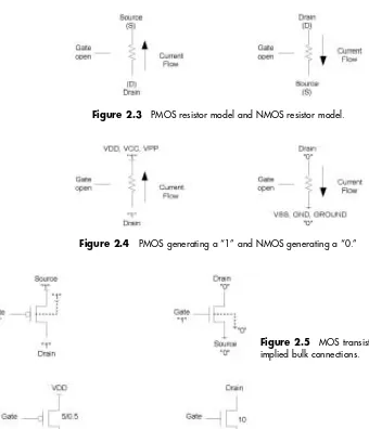
A simpler way to visualize the operation of the transistors is as a resistor when it is “on” (Figure 2.3).
The amount of current that flows through the transistor is limited by the equivalent resistance of the transistor. As we shall see later, the sizing of the tran-sistors directly affects this equivalent resistance. We will use this simpler resistor model in analyzing the operation of the transistors from this point on.
Now let’s consider the case when the source is connected to a static logic level. Generally, logical “1” levels are denoted on a schematic by the highest supply voltage for the design. Typically this high supply voltage would be labeled as VDD, VCC, or perhaps VPP. Conversely, logical “0” levels are denoted on a schematic by the ground level of the chip. VSS, GND, or GROUND are typical names. Under these conditions and with the gates of the transistors open the drain nodes are naturally driven to the same level as the source.
Due to the physical nature and limitations of the PMOS and NMOS devices (not to be discussed here), PMOS transistors are almost always used to establish logical “1” levels and NMOS logical “0” (Figure 2.4), although there are excep-tions, of course. This is why PMOS and NMOS together have been termed “com-plementary”: they complement each other because, together, they simply and reliably generate both logic levels. For this reason, Boolean logic is easily imple-mented using PMOS and NMOS transistors, which is one of the main reasons why CMOS circuitry is so popular today.
Let’s not completely forget the bulk connection mentioned earlier in this section. Remember that the bulk is generally connected to the respective logic levels, and the implied connections to the supply levels are shown in Figure 2.5. The size of the transistor should also be identified on the schematic (Figure 2.6). Each PMOS and NMOS has a length and a width. These dimensions will be
explained in detail in a later chapter, and for now take this as a given. Typically the length of either transistor may not be shown and has a default value. This value is usually the minimum allowable as limited by the process technology, and it is this number that is quoted to specify the technology. For example, a 0.25-mm process typically means the default gate length is 0.25mm and thus is not shown on the schematic because it is redundant information.
In Figure 2.6 the width of the PMOS transistor is 5mm, and that of the NMOS is 10mm. Generally, the width value is always stated first. The PMOS transistor length is 0.5mm, and since the NMOS is not shown, it is assumed to be the default value for the process, which is 0.25mm.
When we start to look at the layout of transistors, it should become more obvious that the resistance of the transistor will decrease and the current drive of the transistor will increase as the width of the transistor is increased or the length of the transistor is decreased. For this chapter, please take this as a given.
The Mos Transistor: The Basic Circuit Structure 9
Figure 2.3 PMOS resistor model and NMOS resistor model.
Figure 2.4 PMOS generating a “1” and NMOS generating a “0.”
Figure 2.5 MOS transistors showing implied bulk connections.
2.2 LOGIC GATES
The majority of schematics today are not filled with transistors. The reasons for this are many, but the main ones are that it is impractical because of the com-plexities of the designs that are undertaken, and that transistors are grouped into what is called a logic gate or “gate.” A logic gate could be confused with the gate of a transistor, but we hope that the context in which the term is used will be sufficiently obvious.
Logic gates are implemented directly or in combination to form Boolean logic functions. Theoretically, almost any Boolean logic function can be imple-mented with a single logic gate, but in practice this is not done. We hope that, after reading this book, you will fully understand why.
In general, most logic functions are implemented in CMOS using inverters, two to four input NANDs, two to four input NORs, and transmission gates. Let’s begin to learn about these gates by understanding the simplest of all logic gates: the inverter.
2.2.1 Inverter
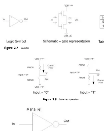
As the name implies, the inverter is the simplest logic gate. Its function is to invert the signal received on the input node to the opposite polarity to the output node (Figure 2.7).
Let’s use our knowledge of transistors. Knowing that the PMOS is “open” when receiving a “0” means that the “1” is driven to the output. In this case the NMOS is off and does not affect the output level. Conversely, by the same rules, a “0” is produced when the input is a “1” (Figure 2.8).
CMOS logic by its very nature is always inverting. Also note that the NMOS and PMOS are never “on” at the same time. This demonstrates the reason why CMOS is a low-power style of circuit design. Once the gate switches state, there is no DC current path between VDD and VSS; such a path, if it existed, would consume DC power.
In specifying the inverter size, now two device sizes are required (Figure 2.9).
• The “P” and “N” identifiers specify the device type. Again, generally the widths are stated first.
• In this case the PMOS transistor width is 2mm, and that of the NMOS is 1mm.
• The PMOS transistor length is 0.5mm, and since the NMOS is not shown it is assumed to be the default value for the process.
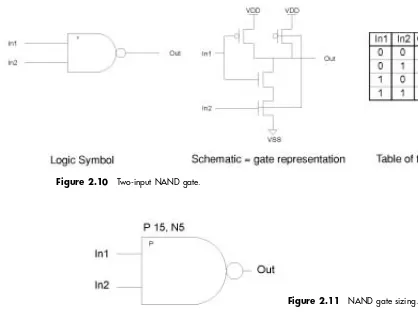
2.2.2 Two-Input NAND Gate
When a logical decision is required to be made between different signals, NAND and NOR gates will do the job. By following the operation of the individual tran-sistors under each input condition in the truth table of Figure 2.10, you will see that the desired output is produced with the transistor configuration shown.
The “Not AND” function (OUT =“0”) is produced when both IN1 and IN2 are both “1.” The requirement for both inputs to be “1” simultaneously is achieved by connecting the two NMOS transistors in series. At the same time, the PMOS transistors are connected in a complementary fashion by being in parallel.
Logic Gates 11
Figure 2.7 Inverter.
Figure 2.8 Inverter operation.
This configuration not only produces the correct functionality from the gate, but also results in eliminating static DC power consumption by ensuring that there is never a condition in which a PMOS path to VDD and an NMOS path to VSS are “on” simultaneously.
Three or more input NAND gates are easily implemented by extending the series connections of the NMOS and the parallel connections of the PMOS transistors.
In specifying the NAND gate transistor sizes, four device sizes are now required. In most cases, however, all PMOS transistors will be the same size and, similarly, all NMOS transistors will be the same size; therefore, once again typi-cally only two values are required (Figure 2.11). This is also true of NOR gates, and indicating sizes on the NOR gate is done in a very similar way.
• The “P” and “N” identifiers specify the device type. Again, generally the widths are stated first.
• In this case the PMOS transistor width is 15mm, and 5mm for the NMOS. • The PMOS and NMOS transistor are assumed to be the default value for the
process.
If distinct sizing for the two separate PMOS transistors is required, typically this would be indicated by a subscript to the “P” identifier such as “P1, P2,” and additional values would be given.
Figure 2.10 Two-input NAND gate.
2.2.3 Two-Input NOR Gate
The NOR gate is the mirror or complementary configuration to the NAND. In the NOR gate the series/parallel connections are reversed between the NMOS and PMOS transistors—the PMOS transistors are in series and the NMOS in parallel (Figure 2.12).
Once again, the potential for DC power consumption is eliminated under all input conditions, and three or more input variations of the NOR are easily made by increasing the series and parallel connections of the PMOS and NMOS transistors, respectively.
Transistor size values are indicated in much the same way as for NAND gates, and a description of a typical convention will not be repeated here.
2.2.4 Complex Gates
As mentioned previously, almost any Boolean logic function can be implemented in a single-stage CMOS logic gate. The term complex gates is the name given to logic gates that have a “complex” function, usually a combination of AND, OR, NAND, and NOR, all implemented in one logic stage.
Because complex gates are implemented in a single stage, in almost all cases power consumption, area, and speed benefits are achieved.
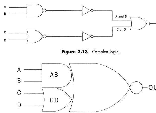
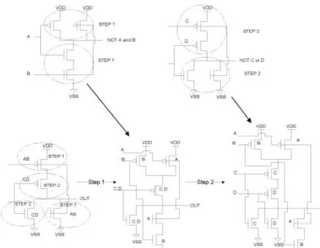
Figure 2.13 is an example of a complex logic function implemented in mul-tiple gates.
If we do a simple transistor count for this logic we find that there are 16 tran-sistors in all with 3 stages of logic. It is very common to find that an engineering schematic would not be designed this way but in a single stage of logic repre-sented by a symbol such as that shown in Figure 2.14.
By combining the inverters with their respective driving gates, you can see that the NAND–inverter combination becomes an AND and the NOR–inverter combination becomes the OR. The output NOR remains the same.
What does the transistor representation of this gate look like? We need this representation to do our layout design.
Logic Gates 13
This type of complex gate is very efficient to use and build, but somehow cumbersome to draw. To determine the transistor representation we analyze the logic starting from the output gate and work backward (i.e., from right to left).
First consider the output of a two-input NOR. The idea is to combine a NAND function representing the AND gate as well as a NOR function repre-senting the OR gate into the output NOR to create the final logic gate.
Why do we use an input NAND instead of AND? Similarly, why NOR instead of OR?
The answer is that the output NOR gate provides an extra stage of logic inversion, which we take advantage of in implementing the final gate. Since there is an inherent inversion in the output NOR gate, we do not need to implement input AND or OR functions; NAND and NOR functions are just what we need. It is wise to work this through and prove it to yourself.
Before we can perform the transistor merging as described later, the prepa-ration step is to determine the logic gates at the input that will be merged into the output gate. This is done by simply inverting the logic at the inputs. In our case we invert the AND to NAND and the OR to a NOR.
1. We replace the AB PMOS transistors with the parallel PMOS transistors of an input NAND and the AB NMOS transistors with the respective series NMOS transistors of the same input NAND.
2. Now we use the same methodology, but for the CD devices. Replace the CD PMOS transistors with the series PMOS transistors of the input NOR and the CD NMOS transistors with the respective parallel NMOS transistors. There—you’re done! (See Figure 2.15.)
If you check the truth table of the final configuration you should find that the 8-transistor logic gate is logically equivalent to the 16-transistor, 3-stage logic function presented earlier.
Figure 2.13 Complex logic.
Use this technique to expand and understand the simplicities of complex gates!
Because of the greater number of transistors for a typical complex gate, indi-vidual transistor sizes may or may not be indicated on the schematic. In most cases each transistor would have a different size, and so transistor sizes are typi-cally omitted from the symbol. Size information must be determined by looking at the transistor-level schematic. Even if sizes are indicated, the mapping of these sizes to the transistor configuration should be manually checked before layout begins.
2.3 TRANSMISSION GATES
Let us consider one more configuration of transistors that may appear in a schematic.
In the case of the inverter, the source of both transistors is connected to a power supply. In the case of combination gates, series connected transistors form part of a chain that eventually connects to a power supply, and thus the transis-tors should be treated similarly to the simple inverter.
The transmission gate is a fairly common case where both the drain and source nodes are used as signals. In this case, the output generally follows the input based on the state of the controls A and B. Note that this configuration allows for noninverting propagation of the input signal, as well as the blocking of the input signal when both control signals disable the PMOS and NMOS transistors. These are powerful features of this gate; transmission gates are used quite frequently and need to be designed carefully (Figure 2.16).
Remember we said that in general PMOS transistors are connected to gen-erate logical “1” levels and NMOS logical “0,” and almost never the reverse. The truth table for the transmission gate shows one of the reasons why this is so. PMOS transistors are able to pass “0” levels, but they do so somewhat unwillingly and degrade the “0” level. The same is true for NMOS transistors and “1” levels. This is what is meant by “Weak Levels” in the truth table. Unless specifically intended, these weak-level conditions are generally avoided in robust logic designs. Usually both controls are implemented such that the transmission gate is either completely “on” or “off” (both transistors) but not halfway.
Understanding the Schematic Connectivity 17
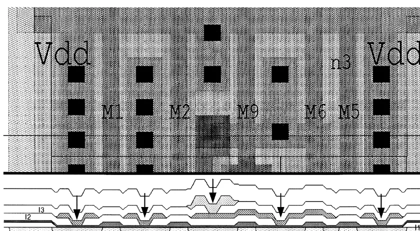
Figure 2.17 Schematic example. TABLE 2.1 Schematic Connections
Schematic
Representation Description
Simple wire connection. These signals are local signals to be routed and implemented within the schematic under consideration.
>> On page connector. A virtual connection is achieved with this symbol. The connection name or node name is used to identify where on the schematic the net is to be routed. In our example the two nodes labeled CLKD are electrically connected but are not visibly connected. Generally, this is done to avoid cluttering the schematic with wires.
Port or pin connector. This symbol identifies a net that enters or exits the schematic under consideration and is part of the “interface” of the schematic to the outside world. These signals may have special considerations attached to them for performance or reliability reasons, so it is important to find out if such conditions exist.
Global connector. We have seen this as the bulk connection to the transistor. A global connector identifies an electrical node that is required internally and externally to the schematic block. The “VDD” net in this case is used everywhere and is global. Again, drawing the wires to show the implied connectivity is impractical.
>
VDD
2.4 UNDERSTANDING THE SCHEMATIC CONNECTIVITY
In implementing the layout of any schematic, there is more to the final design than is explicitly shown. Connections appear on a schematic as a simple line drawn from point A to point B, or a simple connection of two transistors in series or in parallel. In reality, a line represents a signal path that needs to be physically implemented and optimized. Let’s look at an example (Figure 2.17).
2.5 REVIEW OF FUNDAMENTAL ELECTRICAL LAWS
IC layout design is fundamentally the art of implementing an electrical circuit in terms of polygons and shapes, which represent transistors and connections to form the final design. The important concept that we must not forget is that the final design will have electrical characteristics that are very much defined by the characteristics of the physical layout.
The intent of this section is to review a few basic electrical laws and princi-ples that should be understood, so we can establish a good foundation upon which we can move forward and develop efficient and effective layout methodologies.
2.5.1 Ohm’s Law
This is the most basic and fundamental law:
V=I¥R
Voltage =Current ¥Resistance
We have seen that MOS transistors operate as “resistors” when they are “on” or when the gate is “open.” The current flow induced by the opening of the gate creates a voltage swing across the transistor. This demonstrates the application of Ohm’s law! Given the resistance of the transistor and a positive current value, the resulting voltage change is explained by Ohm’s law (Figure 2.18).
Similarly, when the gate is “off” the current is “0.” By Ohm’s law, the voltage change is also “0,” which makes sense since the gate is “closed” and it acts like an open circuit.
In reality, the resistance of the transistor is dynamic, as is the amount of current flowing through the transistor. Therefore, this is a very simplistic model,
Review of Fundamental Electrical Laws 19
but it effectively explains how Ohm’s law works and gives us the concepts behind how a transistor operates.
Ohm’s law is a powerful principle to remember and is the foundation for circuit and layout design alike.
2.5.2 Kirchoff’s Current Law
Kirchoff’s current law is another fundamental law that helps us to explain certain concepts in future chapters. Kirchoff’s current law states that the sum of currents into any electrical node is to zero. In this case currents coming into a node are deemed to be positive currents by convention, and currents passing out of a node are deemed to be negative currents, so their overall sum should equal zero:
I1+I2+I3+. . .+IN=0
Another way of stating the same thing is that the sum of currents into a node must equal the sum of currents out of a node (Figure 2.19).
2.5.3 Resistance
We have already mentioned the concept of resistance without really explaining it in more detail. We have used the resistor to model the transistor in the “on” state. In simple terms resistance can be thought of as the inability (or ability) of a conductor to conduct charge. Using a water analogy, a pipe of large diameter has a lower resistance than a smaller diameter pipe because it can pass a larger amount of water. The cross-sectional area of the pipe is larger in this case. This assumes that the two pipes are the same lengths. As a pipe or conductor increases in length, the resistance also increases.
The convention in IC design for resistance calculation is to characterize each conductor layer in terms of resistance per “square.” One “square” is defined as the condition when the length of the conductor equals the width.
The formula for calculating the resistance of a conductor is
R= r ¥l/w
where “r” is the resistivity of the layer measured in W/䊐,lis the length, and w
is the width of the conductor.
2.5.4 Capacitance
In simple terms, capacitance can be thought of as the amount of charge a body or conductor can hold per unit of voltage between the node in question and another reference node. Using our water analogy, a capacitor should be thought of as a dammed lake that is filled with or emptied of water based on the electrical power needs of consumers.
The amount of capacitance a conductor has is determined by the area of the conductor and how far it is away from the reference node. Again using our water analogy, let’s consider a lake. How much water will it take to fill the lake (think how much charge will it take to charge up the capacitor)? The answer is, it depends on the surface area of the lake and how deep it is.
The tricky part of this concept is that the distance between the reference node, the bottom of the lake, and the surface of the lake determines the depth of the lake. The farther the reference node is away from the conductor, the shallower the lake is. If the reference node is very close, the lake will be deeper and thus the overall capacitance is greater. The concept behind this is that the charge in the conductor is attracted to the reference node by an electric field attraction associated with opposite charges. Closer bodies have larger electric fields and thus larger capacitance values.
There is also a dependency on the material that separates the two nodes. Some materials isolate the attraction to a better degree than others do.
A very simple model for the capacitance of a conductor is calculated as
C= e ¥A/d
where A is the surface area of the specific conductor, dis the physical distance between the conductor and the reference node, and e is a constant repre-senting the characteristics of the insulating layer between the conductor and the reference node.
2.5.5 Delay Calculation
Without going into gory theoretical detail, let us consider a simple example of a inverter driving a wire or conductor. The wire is represented as a single resistor and a lumped capacitance (Figure 2.20).
Our goal is to calculate the delay from IN to node A. The total delay is dependent on two factors:
• The associated switching delay of the inverter. This inverter delay is depen-dent on the size of the resistor and the capacitor. This delay is normally calculated or measured from simulation, so we will not consider it formally here.
• The delay of the wire is due to the resistor and the capacitor. A first-order approximation of the delay through the wire as an independent component is
Delay=R¥C
This simple equation gives us an easy formula to analyze the delay through different wiring scenarios and allows us to make the appropriate trade-offs in laying out the final design.
If it is required to minimize the delay through a given circuit, we need to consider reducing both the resistance and the capacitance of the wire. Using our knowledge of resistance and capacitance, we can optimize our layout to minimize the delay by doing the following:
• Minimizing the length of the conductor. This reduces both the resistance and capacitance terms.
• Optimizing the width of the conductor. Decreasing the width of the conductor decreases the capacitance of the wire; however it increases the resistance!
• Increasing the spacing of the conductor to other reference nodes. This decreases the capacitance of the wire. Usually this means running the wire in areas that are free from other polygons or shapes or using a top metal layer instead of the lower one.
In Chapter 1 we defined in great detail layout design as follows:
The process of creating an accurate physical representation of an engineer-ing drawengineer-ing that conforms to constraints imposed by the manufacturengineer-ing process, the design flow, and the performance requirements shown to be feasible by simulation.
Summarizing once again, a layout designer is a person who knows basic electrical concepts, process limitations, and properties; has a talent for seeing and feeling space and floor plans; and can learn and use various CAD tools.
Let us understand in greater detail the manufacturing process and how it relates layout to the physical representation of the design.
3.1 INTRODUCTION TO CMOS VLSI MANUFACTURING PROCESSES
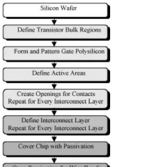
There are many kinds of design processes, but this text discusses only CMOS technologies. We will first discuss the manufacturing order of layers (Figure 3.1) without going into the details of how each step is physically realized.
We start with a bare silicon wafer. Between steps an isolation layer is grown to protect areas that are not to be patterned.
P and N bulk regions are defined by differentiating different areas of the wafer with “wells” or “tubs” of the appropriate type.
The polysilicon that forms the gate areas is added next.
Source and drain areas are defined by diffusing areas on either side of the gate polysilicon. Other active areas such as substrate contacts and guard rings are formed at the same time.
In order for interconnect layers to be connected to the polysilicon and/or active areas, contact holes are created in the isolation layer on top of the layer to be connected.
22
The interconnect layers are deposited and fill the contact holes created in the previous step.
The last layer is called the passivation layer with openings for wire bonding connections. The passivation layer is a glass layer that isolates the chip from the external world.
This diagram is a very simple explanation of the manufacturing process. Different process technologies have significantly different manufacturing steps.
DRAM memories for example have four layers of polysilicon to construct the memory cell capacitor. ASIC designs have only one polysilicon and more layers of metal, which are used to connect many, many logic gates. Using five to six layers of metal, microprocessors, and other complex ASIC designs can be produced (Figure 3.2).
3.2 LAYERS AND CONNECTIVITY
Let us simplify the types of layers that are used and introduce the concept of mask
layers and drawnlayers.
If we analyze most CMOS processes, we find that there are four basic layer types:
1. Conductors:These layers are conducting layers in that they are capable of car-rying signal voltages. Diffusion areas, metal and polysilicon layers, and well layers fall into this category.
Layers and Connectivity 23
2. Isolation layers: These layers are the insulator layers that isolate each con-ductor layer from each other in vertical and horizontal directions. This iso-lation is required in both the vertical and horizontal direction to avoid “short circuits” between separate electrical nodes.
in the passivation layer for bonding pads are another example of a contact layer.
4. Implant layers:These layers do not explicitly define a new layer or contact, but customize or change existing conductor propriety. For example, diffu-sion or active areas for PMOS and NMOS transistors are defined simulta-neously. A P+ mask is used to create P+ implant areas that define certain diffusion areas to P-type by the use of a P-type implant.
Using a combination of these four types of layers, transistor devices, resistors, capacitors, and interconnections are created.
In almost all cases, the number of layers that are drawn by the layout designer has been reduced to the minimum number required for the mask-making process. This minimum number of layers is referred to as the set of drawnlayers. Minimiz-ing the number of drawn layers reduces human error and layer management, as well as the computational requirements of the CAD software.
Themasklayers, or the layer shapes that are translated to the optical masks, are sometimes different from the drawn layers. First, there may be many more mask than drawn layers. In this case, the additional mask layers are automatically generated from the drawn layers.
Additionally, the mask layers may be resized from the drawn layers to account for variances in the manufacturing process. This resizing is also done automatically by the mask-making process.
Note that isolation layers are never drawn but are always implied from the mask layers as part of the manufacturing process.
From this point on any reference to a layer should be interpreted as meaning a drawn layer.
Of course, all of the layer entry is done with sophisticated CAD software, and the subsequent manipulation of layers is also done with computers and com-plicated software.
Every shape that is drawn is entered either as a “polygon” or a “path.” There are subtle differences between the two, which are partly related to the way com-puters handle and process the layout database. There are situations where poly-gons are better suited to layout than paths, and vice versa. These differences will be explained in the next two sections.
3.2.1 The Polygon
As the name implies, a polygon is an N-sided shape that geometrically has N+1 vertices, which define the shape (the computer sees N+1 vertices because there is one vertex that is double counted because it is counted as both the origin and the end point).
The typical uses for polygons are places where the designer has to cover areas that are not necessary a simple rectangle—for example, cell boundaries, tran-sistors, n-wells, contacts, diffusion areas, and transistor gates. In addition, poly-gons are flexible enough to be used to define areas because they can be implemented in various angle modes such as 90 or 45 degrees or in some rare cases as freehand shapes.
The pros of using polygons include the following: • Can be used to enclose an odd-shaped area • Can be easily drawn, added to, or subtracted from
• Can be easily merged with other polygons at the same level of hierarchy and same layer
See some examples of polygons in Figure 3.3. The cons of using polygons include the following:
• Not easy to modify complex polygons for consistency. An example might be when a uniform width is desired and to modify all portions of a polygon is tedious.
• Requires more computer database space compared to a “path” in situations where paths are useable.
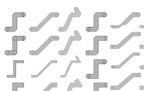
3.2.2 The Path
As the name implies, a path is a shape that is defined by a start and end point, intermediate vertices, and a width value. It is used primarily to connect devices and run signals from point to point because a path has a consistent width.
A path is easily manipulated and uses fewer computer resources than a polygon in terms of data. The vertices define a centerline (or sideline) for the path, and an additional variable defines the path’s width. Path lines can also follow 90-degree, 45-degree, or freehand angle modes.
Paths can be designed as centered, left, or right justified. This means that the shape of the path appears either centered or to the left or right sides of the vertices. An additional attribute of a path is the way the path is ended. The length of the path relative to the start and end points can be fixed, extended beyond the end points by a certain amount, or perhaps rounded.
All of these features need to be implemented with many things in mind: the target manufacturing process, the CAD tools, and design requirements. Some examples of paths are shown in Figure 3.4.
As we can see, the path has a lot of potential in having different termina-tions and vertex formats for different layout styles and design requirements.
An efficient use of paths is to generate layout using multiple paths. Once the desired shape is defined, we can flatten the paths to get polygons (see Figure 3.5). Generating the first version of the layout using paths is much quicker and more efficient. We can still convert the paths to polygons if so desired. The reverse is very limited. A path cannot be generated easily from a polygon.
Depending on the type of layout and the designer’s working habits, the more paths that are used, the more efficient the layout is. Paths are easier to change and contain less computer data. For example, moving a section of a path requires moving one edge. Moving an equivalent section of a polygon requires moving the two edges on each side of the polygon.
Efficient work habits will save time and money in the long run because minimizing the size of the layout database minimizes several other factors:
• Disk space required to store the layout database • Workstation memory usage while working • Screen redraw time
• Workstation CPU time required to process the entire layout database for the mask making process
The only disadvantage of the path is that some CAD tools do not support the merging of a line of paths into one polygon when merging is desired.
3.3 INTRODUCTION TO TRANSISTOR LAYOUT
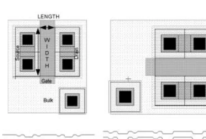
Before we start to discuss the layout of transistors, let us review the schematic fundamentals presented in Chapter 2. The top half of Figure 3.6 shows the basic symbol representations of both PMOS and NMOS transistors. The length and width of the transistors are shown. Also remember that the bulk connection is there, but is hidden from view to avoid cluttering the schematic.
In Chapter 2 we stated that the amount of current flow is determined by the device size. We hinted that the current flow is increased as the width of the device is increased or the length of the device is decreased. Let’s see why this is by under-standing the physical characteristics of the transistor as determined by the layout of the device.
• All four terminals of the transistor are shown and labeled. • The gate of the transistor is defined by a polygon of polysilicon.
• Areas of active or diffusion adjacent to the gate of the transistor define the source and drain areas. Note that the source and drain labels are in fact interchangeable!
• This transistor happens to be a PMOS transistor and the active areas are doped P-type by the P+implant layer.
• This PMOS transistor is located in an N-type well called an N-well. This forms the transistor bulk node.
Introduction to Transistor Layout 29
Figure 3.6 PMOS and NMOS transistors.