3.0 A, Step-Down Switching
Regulator
The LM2596 regulator is monolithic integrated circuit ideally suited for easy and convenient design of a step−down switching regulator (buck converter). It is capable of driving a 3.0 A load with excellent line and load regulation. This device is available in adjustable output version and it is internally compensated to minimize the number of external components to simplify the power supply design.
Since LM2596 converter is a switch−mode power supply, its efficiency is significantly higher in comparison with popular three−terminal linear regulators, especially with higher input voltages. The LM2596 operates at a switching frequency of 150 kHz thus allowing smaller sized filter components than what would be needed with lower frequency switching regulators. Available in a standard 5−lead TO−220 package with several different lead bend options, and D2PAK surface mount package.
The other features include a guaranteed $4% tolerance on output voltage within specified input voltages and output load conditions, and $15% on the oscillator frequency. External shutdown is included, featuring 80 mA (typical) standby current. Self protection features include switch cycle−by−cycle current limit for the output switch, as well as thermal shutdown for complete protection under fault conditions.
Features
•
Adjustable Output Voltage Range 1.23 V − 37 V•
Guaranteed 3.0 A Output Load Current•
Wide Input Voltage Range up to 40 V•
150 kHz Fixed Frequency Internal Oscillator•
TTL Shutdown Capability•
Low Power Standby Mode, typ 80 mA•
Thermal Shutdown and Current Limit Protection•
Internal Loop Compensation•
Moisture Sensitivity Level (MSL) Equals 1•
Pb−Free Packages are Available Applications•
Simple High−Efficiency Step−Down (Buck) Regulator•
Efficient Pre−Regulator for Linear Regulators•
On−Card Switching Regulators•
Positive to Negative Converter (Buck−Boost)See detailed ordering and shipping information in the package dimensions section on page 23 of this data sheet.
ORDERING INFORMATION 1
5
TO−220 TV SUFFIX CASE 314B
1
5
Heatsink surface connected to Pin 3
TO−220 T SUFFIX CASE 314D
Pin 1. Vin 2. Output 3. Ground 4. Feedback 5. ON/OFF
D2PAK D2T SUFFIX CASE 936A
Heatsink surface (shown as terminal 6 in case outline drawing) is connected to Pin 3
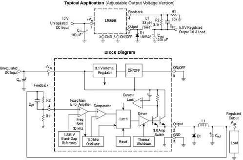
1 5
Figure 1. Typical Application and Internal Block Diagram
12 V Unregulated DC Input
L1 33 mH
GND +Vin
1 Cin
100 mF
3 5 ON/OFF
Output 2 Feedback 4
D1
1N5822 Cout
220 mF
Typical Application (Adjustable Output Voltage Version)
Block Diagram
Unregulated DC Input
+Vin
1
Cout Feedback
4 Cin
L1
D1 R2
R1
Output 2 GND 3 ON/OFF 5
Reset Latch
Thermal Shutdown 150 kHz
Oscillator 1.235 V
Band-Gap Reference
Freq Shift 30 kHz
Comparator Fixed Gain
Error Amplifier
Current Limit
Driver
3.0 Amp Switch ON/OFF
3.1 V Internal Regulator
Regulated Output
Vout
Load
LM2596
5.0 V Regulated Output 3.0 A Load R1
R2 3.1k
1.0k
CFF
CFF
MAXIMUM RATINGS
Rating Symbol Value Unit
Maximum Supply Voltage Vin 45 V
ON/OFF Pin Input Voltage − −0.3 V ≤ V ≤ +Vin V
Output Voltage to Ground (Steady−State) − −1.0 V
Power Dissipation
Case 314B and 314D (TO−220, 5−Lead) PD Internally Limited W
Thermal Resistance, Junction−to−Ambient RqJA 65 °C/W
Thermal Resistance, Junction−to−Case RqJC 5.0 °C/W
Case 936A (D2PAK) P
D Internally Limited W
Thermal Resistance, Junction−to−Ambient RqJA 70 °C/W
Thermal Resistance, Junction−to−Case RqJC 5.0 °C/W
Storage Temperature Range Tstg −65 to +150 °C
Minimum ESD Rating (Human Body Model: C = 100 pF, R = 1.5 kW) − 2.0 kV
Lead Temperature (Soldering, 10 seconds) − 260 °C
Maximum Junction Temperature TJ 150 °C
PIN FUNCTION DESCRIPTION
Pin Symbol Description (Refer to Figure 1)
1 Vin This pin is the positive input supply for the LM2596 step−down switching regulator. In order to minimize voltage transi-ents and to supply the switching currtransi-ents needed by the regulator, a suitable input bypass capacitor must be present (Cin in Figure 1).
2 Output This is the emitter of the internal switch. The saturation voltage Vsat of this output switch is typically 1.5 V. It should be kept in mind that the PCB area connected to this pin should be kept to a minimum in order to minimize coupling to sensitive circuitry.
3 GND Circuit ground pin. See the information about the printed circuit board layout.
4 Feedback This pin is the direct input of the error amplifier and the resistor network R2, R1 is connected externally to allow pro-gramming of the output voltage.
5 ON/OFF It allows the switching regulator circuit to be shut down using logic level signals, thus dropping the total input supply current to approximately 80 mA. The threshold voltage is typically 1.6 V. Applying a voltage above this value (up to +Vin) shuts the regulator off. If the voltage applied to this pin is lower than 1.6 V or if this pin is left open, the regulator will be in the “on” condition.
OPERATING RATINGS (Operating Ratings indicate conditions for which the device is intended to be functional, but do not guarantee specific performance limits. For guaranteed specifications and test conditions, see the Electrical Characteristics.)
Rating Symbol Value Unit
Operating Junction Temperature Range TJ −40 to +125 °C
SYSTEM PARAMETERS
ELECTRICAL CHARACTERISTICS Specifications with standard type face are for TJ = 25°C, and those with boldface type apply
over full Operating Temperature Range −40°C to +125°C
Characteristics Symbol Min Typ Max Unit
LM2596 (Note 1, Test Circuit Figure 15)
Feedback Voltage (Vin = 12 V, ILoad = 0.5 A, Vout = 5.0 V, ) VFB_nom 1.23 V
Feedback Voltage (8.5 V ≤ Vin≤ 40 V, 0.5 A ≤ ILoad ≤ 3.0 A, Vout = 5.0 V) VFB 1.193
1.18
1.267
1.28
V
Efficiency (Vin = 12 V, ILoad = 3.0 A, Vout = 5.0 V) η − 73 − %
Characteristics Symbol Min Typ Max Unit
Feedback Bias Current (Vout = 5.0 V) Ib 25 100
200
nA
Oscillator Frequency (Note 2) fosc 135
120
150 165
180
kHz
Saturation Voltage (Iout = 3.0 A, Notes 3 and 4) Vsat 1.5 1.8
2.0
V
Max Duty Cycle “ON” (Note 4) DC 95 %
Current Limit (Peak Current, Notes 2 and 3) ICL 4.2
3.5
5.6 6.9
7.5
A
Output Leakage Current (Notes 5 and 6) Output = 0 V
Output = −1.0 V
IL
0.5 6.0
2.0 20
mA
Quiescent Current (Note 5) IQ 5.0 10 mA
Standby Quiescent Current (ON/OFF Pin = 5.0 V (“OFF”)) (Note 6)
Istby 80 200
250
mA
ON/OFF PIN LOGIC INPUT
Threshold Voltage 1.6 V
Vout = 0 V (Regulator OFF) VIH 2.2
2.4
V
Vout = Nominal Output Voltage (Regulator ON) VIL 1.0
0.8
V
ON/OFF Pin Input Current
ON/OFF Pin = 5.0 V (Regulator OFF) IIH − 15 30 mA
ON/OFF Pin = 0 V (regulator ON) IIL − 0.01 5.0 mA
1. External components such as the catch diode, inductor, input and output capacitors can affect switching regulator system performance. When the LM2596 is used as shown in the Figure 15 test circuit, system performance will be as shown in system parameters section. 2. The oscillator frequency reduces to approximately 30 kHz in the event of an output short or an overload which causes the regulated output
voltage to drop approximately 40% from the nominal output voltage. This self protection feature lowers the average dissipation of the IC by lowering the minimum duty cycle from 5% down to approximately 2%.
3. No diode, inductor or capacitor connected to output (Pin 2) sourcing the current. 4. Feedback (Pin 4) removed from output and connected to 0 V.
CURRENT
(mA)
TYPICAL PERFORMANCE CHARACTERISTICS (Circuit of Figure 15)
V out
, OUTPUT
VOL
TAGE CHANGE (%)
V out
, OUTPUT
VOL
TAGE CHANGE (%)
CURRENT
(
I O
, OUTPUT
CURRENT
(A)
TJ, JUNCTION TEMPERATURE (°C) Vin, INPUT VOLTAGE (V)
INPUT
- OUTPUT
DIFFERENTIAL
(V)
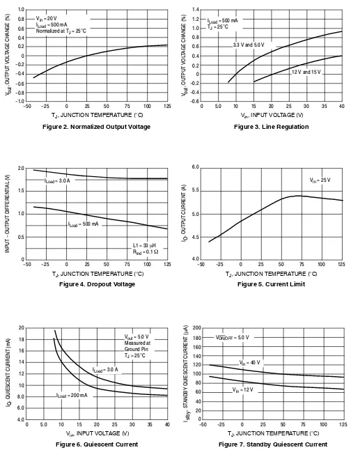
TJ, JUNCTION TEMPERATURE (°C) Figure 2. Normalized Output Voltage
TJ, JUNCTION TEMPERATURE (°C)
Figure 3. Line Regulation
Figure 4. Dropout Voltage Figure 5. Current Limit
ILoad = 3.0 A
Vin = 40 V L1 = 33 mH
Rind = 0.1 W
ILoad = 500 mA
ILoad = 3.0 A
Vout = 5.0 V Measured at Ground Pin TJ = 25°C
VON/OFF = 5.0 V
µ
A)
1.0
0.6
0.2 0 -0.2 -0.4
-1.0
1.4 1.2 1.0 0.8 0.6 0.4 0.2 0 -0.2 -0.4 -0.6
2.0
1.5
1.0
0.5
0
6.0
5.5
5.0
4.5
4.0
20
18
16
14
12
200 180 160 140 120 100 125
100 75 50 25 0 -25
-50 0 5.0 10 15 20 25 30 35 40
125 100 75 50 25 0 -25
-50 -50 -25 0 25 50 75 100 125
-0.8 -0.6 0.4
0.8 Vin = 20 V
ILoad = 500 mA
Normalized at TJ = 25°C
ILoad = 500 mA
TJ = 25°C
3.3 V and 5.0 V
12 V and 15 V
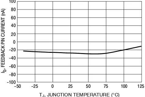
Vsat , SA TURA TION VOL TAGE (V) 2.0 2.5 3.0 4.0 I b
, FEEDBACK PIN CURRENT
(nA) , ST ANDBY QUIESCENT CURRENT ( µ A) I stby , INPUT VOL TAGE (V)
TJ, JUNCTION TEMPERATURE (°C) SWITCH CURRENT (A)
NORMALIZED FREQUENCY
(%)
TJ, JUNCTION TEMPERATURE (°C) Figure 8. Standby Quiescent Current
Vin, INPUT VOLTAGE (V)
Figure 9. Switch Saturation Voltage
Figure 10. Switching Frequency Figure 11. Minimum Supply Operating Voltage
Figure 12. Feedback Pin Current
TJ = 25°C
200 180 140 120 100 80 60 40 20 0 1.6 1.4 1.2 1.0 0.8 0.6 0.4 0.2 0 5.0 4.5 3.5 1.5 1.0 0.5 0 40 30 25 20 15 10 5
0 0 0.5 1.0 1.5 2.0 3.0
125 100 75 50 25 0 -25 -50
TJ, JUNCTION TEMPERATURE (°C)
100 80 60 40 20 0 -20 -40 -60 -80 -100 125 100 75 50 25 0 -25 -50 160 35 2.5
-40°C
25°C
125°C
Vout' 1.23 V
ILoad = 500 mA
TYPICAL PERFORMANCE CHARACTERISTICS (Circuit of Figure 15)
Vin −9.0 −8.0 −7.0 −6.0 −5.0 −4.0 −3.0 −2.0 −1.0 0.0 1.0
−50 −25 0 25 50 75 100 125
2.0 A
0 0 A
B
C
100ms/div 2 ms/div
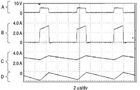
Figure 13. Switching Waveforms Figure 14. Load Transient Response
Vout = 5 V
A: Output Pin Voltage, 10 V/div
B: Switch Current, 2.0 A/div
C: Inductor Current, 2.0 A/div, AC−Coupled D: Output Ripple Voltage, 50 mV/div, AC−Coupled Horizontal Time Base: 5.0ms/div
10 V
0
4.0 A
2.0 A
100 mV Output Voltage Change
0
3.0 A
2.0 A
1.0 A
0 4.0 A
- 100 mV
Load Current
TYPICAL PERFORMANCE CHARACTERISTICS (Circuit of Figure 15)
D
Figure 15. Typical Test Circuit
D1 1N5822
L1 33 mH Output
2 4
Feedback
Cout
220 mF Cin
100 mF
LM2596 1
5
3 GND ON/OFF
Vin
Load Vout
5,000 V
Adjustable Output Voltage Versions
Vout+Vref
ǒ
1.0) R2 R1Ǔ
R2+R1
ǒ
Vout Vref 1.0Ǔ
Where Vref = 1.23 V, R1
between 1.0 k and 5.0 k
R2
R1 8.5 V - 40 V
Unregulated DC Input
PCB LAYOUT GUIDELINES
As in any switching regulator, the layout of the printed circuit board is very important. Rapidly switching currents associated with wiring inductance, stray capacitance and parasitic inductance of the printed circuit board traces can generate voltage transients which can generate electromagnetic interferences (EMI) and affect the desired operation. As indicated in the Figure 15, to minimize inductance and ground loops, the length of the leads indicated by heavy lines should be kept as short as possible. For best results, single−point grounding (as indicated) or ground plane construction should be used.
On the other hand, the PCB area connected to the Pin 2 (emitter of the internal switch) of the LM2596 should be kept to a minimum in order to minimize coupling to sensitive circuitry.
Another sensitive part of the circuit is the feedback. It is important to keep the sensitive feedback wiring short. To assure this, physically locate the programming resistors near to the regulator, when using the adjustable version of the LM2596 regulator.
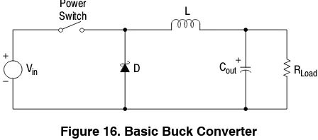
DESIGN PROCEDURE Buck Converter Basics
The LM2596 is a “Buck” or Step−Down Converter which is the most elementary forward−mode converter. Its basic schematic can be seen inFigure 16.
The operation of this regulator topology has two distinct time periods. The first one occurs when the series switch is on, the input voltage is connected to the input of the inductor. The output of the inductor is the output voltage, and the rectifier (or catch diode) is reverse biased. During this period, since there is a constant voltage source connected across the inductor, the inductor current begins to linearly ramp upwards, as described by the following equation:
IL(on)+
ǒ
VIN*VOUTǓ
ton LDuring this “on” period, energy is stored within the core material in the form of magnetic flux. If the inductor is properly designed, there is sufficient energy stored to carry the requirements of the load during the “off” period.
Figure 16. Basic Buck Converter
D
Vin RLoad
L
Cout
Power Switch
The next period is the “off” period of the power switch. When the power switch turns off, the voltage across the inductor reverses its polarity and is clamped at one diode voltage drop below ground by the catch diode. The current now flows through the catch diode thus maintaining the load current loop. This removes the stored energy from the inductor. The inductor current during this time is:
IL(off)+
ǒ
VOUT*VDǓ
toff LThis period ends when the power switch is once again turned on. Regulation of the converter is accomplished by varying the duty cycle of the power switch. It is possible to describe the duty cycle as follows:
d+tonT , where T is the period of switching.
For the buck converter with ideal components, the duty cycle can also be described as:
d+VVout
in
Figure 17 shows the buck converter, idealized waveforms of the catch diode voltage and the inductor current.
Power Switch
Figure 17. Buck Converter Idealized Waveforms
Power Switch Off
Power Switch Off
Power Switch On Power
Switch On Von(SW)
VD(FWD)
Time
Time ILoad(AV)
Imin
Ipk
Diode Diode
Power Switch
Diode V
oltage
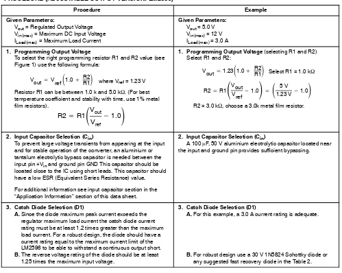
PROCEDURE (ADJUSTABLE OUTPUT VERSION:LM2596)
Procedure Example
Given Parameters:
Vout = Regulated Output Voltage Vin(max) = Maximum DC Input Voltage ILoad(max) = Maximum Load Current
Given Parameters:
Vout = 5.0 V Vin(max) = 12 V ILoad(max) = 3.0 A
1. Programming Output Voltage
To select the right programming resistor R1 and R2 value (see Figure 1) use the following formula:
Resistor R1 can be between 1.0 k and 5.0 kW. (For best temperature coefficient and stability with time, use 1% metal film resistors).
Vout+Vref
ǒ
1.0) R2R1Ǔ
R2+R1
ǒ
VoutVref*1.0
Ǔ
where Vref = 1.23 V1. Programming Output Voltage (selecting R1 and R2) Select R1 and R2:
R2 = 3.0 kW, choose a 3.0k metal film resistor. R2+R1
ǒ
VoutVref*1.0
Ǔ
+ǒ
5 V1.23 V*1.0
Ǔ
Vout+1.23ǒ
1.0) R2R1
Ǔ
Select R1 = 1.0 kW2. Input Capacitor Selection (Cin)
To prevent large voltage transients from appearing at the input and for stable operation of the converter, an aluminium or tantalum electrolytic bypass capacitor is needed between the input pin +Vin and ground pin GND This capacitor should be located close to the IC using short leads. This capacitor should have a low ESR (Equivalent Series Resistance) value.
For additional information see input capacitor section in the “Application Information” section of this data sheet.
2. Input Capacitor Selection (Cin)
A 100 mF, 50 V aluminium electrolytic capacitor located near the input and ground pin provides sufficient bypassing.
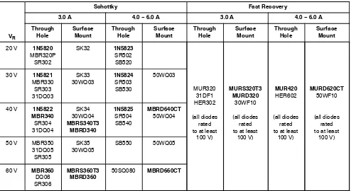
3. Catch Diode Selection (D1)
A.Since the diode maximum peak current exceeds the regulator maximum load current the catch diode current rating must be at least 1.2 times greater than the maximum load current. For a robust design, the diode should have a current rating equal to the maximum current limit of the LM2596 to be able to withstand a continuous output short.
B.The reverse voltage rating of the diode should be at least 1.25 times the maximum input voltage.
3. Catch Diode Selection (D1)
A.For this example, a 3.0 A current rating is adequate.
PROCEDURE (ADJUSTABLE OUTPUT VERSION:LM2596) (CONTINUED)
Procedure Example
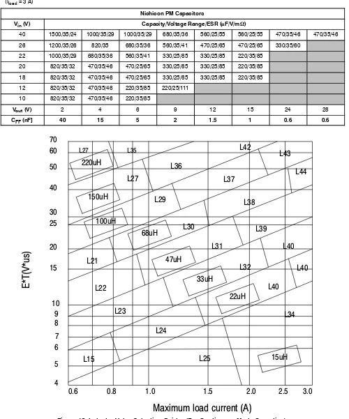
4. Inductor Selection (L1)
A.Use the following formula to calculate the inductor Volt x microsecond [V x ms] constant:
B.Match the calculated E x T value with the corresponding number on the vertical axis of the Inductor Value Selection Guide shown inFigure 18. This E x T constant is a
measure of the energy handling capability of an inductor and is dependent upon the type of core, the core area, the number of turns, and the duty cycle.
C.Next step is to identify the inductance region intersected by the E x T value and the maximum load current value on the horizontal axis shown inFigure 18.
D.Select an appropriate inductor from Table 3. The inductor chosen must be rated for a switching
frequency of 150 kHz and for a current rating of 1.15 x ILoad. The inductor current rating can also be determined by calculating the inductor peak current:
where ton is the “on” time of the power switch and E T+ǒVIN*VOUT*VSATǓ
VOUT)VD VIN*VSAT)VD
1000 150 kHzǒV msǓ
Ip(max)+ILoad(max))
ǒ
Vin *Vout
Ǔ
ton 2Lton + VoutV in
x 1.0 fosc
4. Inductor Selection (L1)
A.Calculate E x T [V x ms] constant:
B.E x T = 27 [V x ms]
C.ILoad(max) = 3.0 A Inductance Region = L40
D.Proper inductor value = 33 mH Choose the inductor from Table 3. E T+ǒ12*5*1.5Ǔ 5)0.5
12*5)0.5 1000
150 kHzǒV msǓ
E T+ǒ5.5Ǔ 5.5
7.5 6.6ǒV msǓ
5. Output Capacitor Selection (Cout)
A.Since the LM2596 is a forward−mode switching regulator
with voltage mode control, its open loop has 2−pole−1−zero frequency characteristic. The loop stability is determined by the output capacitor (capacitance, ESR) and inductance values.
For stable operation use recommended values of the output capacitors in Table 1.
Low ESR electrolytic capacitors between 220uFand 1500uF provide best results.
B.The capacitors voltage rating should be at least 1.5 times greater than the output voltage, and often much higher voltage rating is needed to satisfy low ESR requirement
5. Output Capacitor Selection (Cout)
A.In this example is recommended Nichicon PM capacitors: 470 mF/35 V or 220 mF/35 V
6. Feedforward Capacitor (CFF)
It provides additional stability mainly for higher input voltages. For Cff selection use Table 1. The compensation capacitor between 0.6 nF and 40 nF is wired in parallel with the output voltage setting resistor R2, The capacitor type can be ceramic, plastic, etc..
6. Feedforward Capacitor (CFF)
LM2596 Series Buck Regulator Design Procedures (continued)
Table 1. RECOMMENDED VALUES OF THE OUTPUT CAPACITOR AND FEEDFORWARD CAPACITOR (Iload = 3 A)
Nichicon PM Capacitors
Vin (V) Capacity/Voltage Range/ESR (mF/V/mW)
40 1500/35/24 1000/35/29 1000/35/29 680/35/36 560/25/55 560/25/55 470/35/46 470/35/46
26 1200/35/26 820/35 680/35/36 560/35/41 470/25/65 470/25/65 330/35/60
22 1000/35/29 680/35/36 560/35/41 330/25/85 330/25/85 220/35/85
20 820/35/32 470/35/46 470/25/65 330/25/85 330/25/85 220/35/85
18 820/35/32 470/35/46 470/25/65 330/25/85 330/25/85 220/35/85
12 820/35/32 470/35/46 220/35/85 220/25/111
10 820/35/32 470/35/46 220/35/85
Vout (V) 2 4 6 9 12 15 24 28
CFF (nF] 40 15 5 2 1.5 1 0.6 0.6
15uH
22uH
33uH
47uH
68uH
100uH
150uH
220uH
L35 L27
L36
L27
L42
L43
L44
L37
L38
L30
L29
L21
L22
L31
L39
L40
L32
L23
L15
L24
L40
L40
L25
L34
6
7
8
9
10
15
20
25
30
40
50
60
70
Table 2. DIODE SELECTION
VR
Schottky Fast Recovery
3.0 A 4.0 − 6.0 A 3.0 A 4.0 − 6.0 A
Through Hole
Surface Mount
Through Hole
Surface Mount
Through Hole
Surface Mount
Through Hole
Surface Mount
20 V 1N5820
MBR320P SR302
SK32 1N5823
SR502 SB520
MUR320 31DF1 HER302 (all diodes
rated to at least
100 V)
MURS320T3 MURD320
30WF10 (all diodes
rated to at least
100 V)
MUR420
HER602
(all diodes rated to at least
100 V)
MURD620CT
50WF10
(all diodes rated to at least
100 V)
30 V 1N5821
MBR330 SR303 31DQ03
SK33 30WQ03
1N5824
SR503 SB530
50WQ03
40 V 1N5822
MBR340
SR304 31DQ04
SK34 30WQ04
MBRS340T3 MBRD340
1N5825
SR504 SB540
MBRD640CT
50WQ04
50 V MBR350
31DQ05 SR305
SK35 30WQ05
SB550 50WQ05
60 V MBR360
DQ06 SR306
MBRS360T3 MBRD360
50SQ080 MBRD660CT
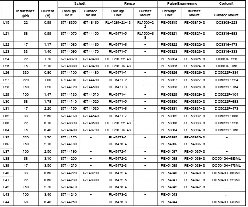
Table 3. INDUCTOR MANUFACTURERS PART NUMBERS
Inductance (mH)
Current (A)
Schott Renco Pulse Engineering Coilcraft
Through Hole
Surface Mount
Through Hole
Surface Mount
Through Hole
Surface
Mount Surface Mount
L15 22 0.99 67148350 67148460 RL−1284−22−43 RL1500−2 2
PE−53815 PE−53815−S DO3308−223
L21 68 0.99 67144070 67144450 RL−5471−5 RL1500−6 8
PE−53821 PE−53821−S DO3316−683
L22 47 1.17 67144080 67144460 RL−5471−6 − PE−53822 PE−53822−S DO3316−473
L23 33 1.40 67144090 67144470 RL−5471−7 − PE−53823 PE−53823−S DO3316−333
L24 22 1.70 67148370 67148480 RL−1283−22−43 − PE−53824 PE−53825−S DO3316−223
L25 15 2.10 67148380 67148490 RL−1283−15−43 − PE−53825 PE−53824−S DO3316−153
L26 330 0.80 67144100 67144480 RL−5471−1 − PE−53826 PE−53826−S DO5022P−334
L27 220 1.00 67144110 67144490 RL−5471−2 − PE−53827 PE−53827−S DO5022P−224
L28 150 1.20 67144120 67144500 RL−5471−3 − PE−53828 PE−53828−S DO5022P−154
L29 100 1.47 67144130 67144510 RL−5471−4 − PE−53829 PE−53829−S DO5022P−104
L30 68 1.78 67144140 67144520 RL−5471−5 − PE−53830 PE−53830−S DO5022P−683
L31 47 2.20 67144150 67144530 RL−5471−6 − PE−53831 PE−53831−S DO5022P−473
L32 33 2.50 67144160 67144540 RL−5471−7 − PE−53932 PE−53932−S DO5022P−333
L33 22 3.10 67148390 67148500 RL−1283−22−43 − PE−53933 PE−53933−S DO5022P−223
L34 15 3.40 67148400 67148790 RL−1283−15−43 − PE−53934 PE−53934−S DO5022P−153
L35 220 1.70 67144170 − RL−5473−1 − PE−53935 PE−53935−S −
L36 150 2.10 67144180 − RL−5473−4 − PE−54036 PE−54036−S −
L37 100 2.50 67144190 − RL−5472−1 − PE−54037 PE−54037−S −
L38 68 3.10 67144200 − RL−5472−2 − PE−54038 PE−54038−S DO5040H−683ML
L39 47 3.50 67144210 − RL−5472−3 − PE−54039 PE−54039−S DO5040H−473ML
L40 33 3.50 67144220 67148290 RL−5472−4 − PE−54040 PE−54040−S DO5040H−333ML
L41 22 3.50 67144230 67148300 RL−5472−5 − PE−54041 PE−54041−S DO5040H−223ML
L42 150 2.70 67148410 − RL−5473−4 − PE−54042 PE−54042−S −
L43 100 3.40 67144240 − RL−5473−2 − PE−54043 -
APPLICATION INFORMATION
EXTERNAL COMPONENTS
Input Capacitor (Cin)
The Input Capacitor Should Have a Low ESR
For stable operation of the switch mode converter a low ESR (Equivalent Series Resistance) aluminium or solid tantalum bypass capacitor is needed between the input pin and the ground pin, to prevent large voltage transients from appearing at the input. It must be located near the regulator and use short leads. With most electrolytic capacitors, the capacitance value decreases and the ESR increases with lower temperatures. For reliable operation in temperatures below −25°C larger values of the input capacitor may be needed. Also paralleling a ceramic or solid tantalum capacitor will increase the regulator stability at cold temperatures.
RMS Current Rating of Cin
The important parameter of the input capacitor is the RMS current rating. Capacitors that are physically large and have large surface area will typically have higher RMS current ratings. For a given capacitor value, a higher voltage electrolytic capacitor will be physically larger than a lower voltage capacitor, and thus be able to dissipate more heat to the surrounding air, and therefore will have a higher RMS current rating. The consequence of operating an electrolytic capacitor beyond the RMS current rating is a shortened operating life. In order to assure maximum capacitor operating lifetime, the capacitor’s RMS ripple current rating should be:
Irms > 1.2 x d x ILoad
where d is the duty cycle, for a buck regulator d+tonT +VVout
in and d+tonT + |Vout|
|Vout| ) Vin for a buck*boost regulator.
Output Capacitor (Cout)
For low output ripple voltage and good stability, low ESR output capacitors are recommended. An output capacitor has two main functions: it filters the output and provides
regulator loop stability. The ESR of the output capacitor and the peak−to−peak value of the inductor ripple current are the main factors contributing to the output ripple voltage value. Standard aluminium electrolytics could be adequate for some applications but for quality design, low ESR types are recommended.
An aluminium electrolytic capacitor’s ESR value is related to many factors such as the capacitance value, the voltage rating, the physical size and the type of construction. In most cases, the higher voltage electrolytic capacitors have lower ESR value. Often capacitors with much higher voltage ratings may be needed to provide low ESR values that, are required for low output ripple voltage.
Feedfoward Capacitor
(Adjustable Output Voltage Version)
This capacitor adds lead compensation to the feedback loop and increases the phase margin for better loop stability. For CFF selection, see the design procedure section. The Output Capacitor Requires an ESR Value That Has an Upper and Lower Limit
As mentioned above, a low ESR value is needed for low output ripple voltage, typically 1% to 2% of the output voltage. But if the selected capacitor’s ESR is extremely low (below 0.05 W), there is a possibility of an unstable feedback loop, resulting in oscillation at the output. This situation can occur when a tantalum capacitor, that can have a very low ESR, is used as the only output capacitor.
At Low Temperatures, Put in Parallel Aluminium Electrolytic Capacitors with Tantalum Capacitors
Catch Diode
Locate the Catch Diode Close to the LM2596
The LM2596 is a step−down buck converter; it requires a fast diode to provide a return path for the inductor current when the switch turns off. This diode must be located close to the LM2596 using short leads and short printed circuit traces to avoid EMI problems.
Use a Schottky or a Soft Switching Ultra−Fast Recovery Diode
Since the rectifier diodes are very significant sources of losses within switching power supplies, choosing the rectifier that best fits into the converter design is an important process. Schottky diodes provide the best performance because of their fast switching speed and low forward voltage drop.
They provide the best efficiency especially in low output voltage applications (5.0 V and lower). Another choice could be Fast−Recovery, or Ultra−Fast Recovery diodes. It has to be noted, that some types of these diodes with an abrupt turnoff characteristic may cause instability or EMI troubles.
A fast−recovery diode with soft recovery characteristics can better fulfill some quality, low noise design requirements. Table 2 provides a list of suitable diodes for the LM2596 regulator. Standard 50/60 Hz rectifier diodes, such as the 1N4001 series or 1N5400 series are NOT suitable.
Inductor
The magnetic components are the cornerstone of all switching power supply designs. The style of the core and the winding technique used in the magnetic component’s design has a great influence on the reliability of the overall power supply.
Using an improper or poorly designed inductor can cause high voltage spikes generated by the rate of transitions in current within the switching power supply, and the possibility of core saturation can arise during an abnormal operational mode. Voltage spikes can cause the semiconductors to enter avalanche breakdown and the part can instantly fail if enough energy is applied. It can also cause significant RFI (Radio Frequency Interference) and EMI (Electro−Magnetic Interference) problems.
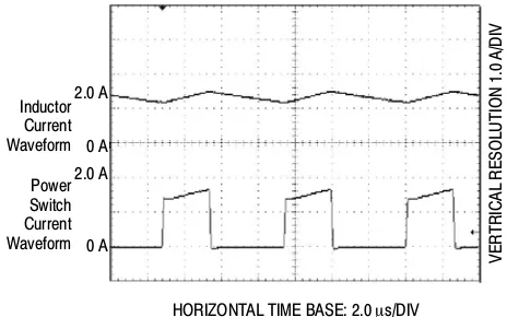
Continuous and Discontinuous Mode of Operation
The LM2596 step−down converter can operate in both the continuous and the discontinuous modes of operation. The regulator works in the continuous mode when loads are relatively heavy, the current flows through the inductor
ripple voltage. On the other hand it does require larger inductor values to keep the inductor current flowing continuously, especially at low output load currents and/or high input voltages.
To simplify the inductor selection process, an inductor selection guide for the LM2596 regulator was added to this data sheet (Figure18). This guide assumes that the regulator is operating in the continuous mode, and selects an inductor that will allow a peak−to−peak inductor ripple current to be a certain percentage of the maximum design load current. This percentage is allowed to change as different design load currents are selected. For light loads (less than approximately 300 mA) it may be desirable to operate the regulator in the discontinuous mode, because the inductor value and size can be kept relatively low. Consequently, the percentage of inductor peak−to−peak current increases. This discontinuous mode of operation is perfectly acceptable for this type of switching converter. Any buck regulator will be forced to enter discontinuous mode if the load current is light enough.
HORIZONTAL TIME BASE: 2.0 ms/DIV
Figure 19. Continuous Mode Switching Current Waveforms
VER
TRICAL
RESOLUTION 1.0
A/DIV
2.0 A
0 A 2.0 A
0 A Inductor
Current Waveform
Power Switch Current Waveform
Selecting the Right Inductor Style
Some important considerations when selecting a core type are core material, cost, the output power of the power supply, the physical volume the inductor must fit within, and the amount of EMI (Electro−Magnetic Interference) shielding that the core must provide. The inductor selection guide covers different styles of inductors, such as pot core, E−core, toroid and bobbin core, as well as different core materials such as ferrites and powdered iron from different manufacturers.
interference between two or more of the regulator circuits, especially at high currents due to mutual coupling. A toroid, pot core or E−core (closed magnetic structure) should be used in such applications.
Do Not Operate an Inductor Beyond its Maximum Rated Current
Exceeding an inductor’s maximum current rating may cause the inductor to overheat because of the copper wire losses, or the core may saturate. Core saturation occurs when the flux density is too high and consequently the cross sectional area of the core can no longer support additional lines of magnetic flux.
This causes the permeability of the core to drop, the inductance value decreases rapidly and the inductor begins to look mainly resistive. It has only the DC resistance of the winding. This can cause the switch current to rise very rapidly and force the LM2596 internal switch into cycle−by−cycle current limit, thus reducing the DC output load current. This can also result in overheating of the
inductor and/or the LM2596. Different inductor types have different saturation characteristics, and this should be kept in mind when selecting an inductor.
0.4 A
0 A
0.4 A
0 A Inductor
Current Waveform
Power Switch Current Waveform
Figure 20. Discontinuous Mode Switching Current Waveforms
VER
TICAL
RESOLUTION 200 mA/DIV
HORIZONTAL TIME BASE: 2.0 ms/DIV
GENERAL RECOMMENDATIONS Output Voltage Ripple and Transients
Source of the Output Ripple
Since the LM2596 is a switch mode power supply regulator, its output voltage, if left unfiltered, will contain a sawtooth ripple voltage at the switching frequency. The output ripple voltage value ranges from 0.5% to 3% of the output voltage. It is caused mainly by the inductor sawtooth ripple current multiplied by the ESR of the output capacitor.
Short Voltage Spikes and How to Reduce Them
The regulator output voltage may also contain short voltage spikes at the peaks of the sawtooth waveform (see Figure 21). These voltage spikes are present because of the fast switching action of the output switch, and the parasitic inductance of the output filter capacitor. There are some other important factors such as wiring inductance, stray capacitance, as well as the scope probe used to evaluate these transients, all these contribute to the amplitude of these spikes. To minimize these voltage spikes, low inductance capacitors should be used, and their lead lengths must be kept short. The importance of quality printed circuit board layout design should also be highlighted.
Unfiltered Output Voltage Filtered Output Voltage
HORIZONTAL TIME BASE: 5.0 ms/DIV
Figure 21. Output Ripple Voltage Waveforms
VER
TRICAL
Voltage spikes caused by switching action of the output switch and the parasitic inductance of the output capacitor
RESOLUTION 20 mV/DIV
Minimizing the Output Ripple
In order to minimize the output ripple voltage it is possible to enlarge the inductance value of the inductor L1 and/or to use a larger value output capacitor. There is also another way to smooth the output by means of an additional LC filter (20
mH, 100 mF), that can be added to the output (see Figure 30) to further reduce the amount of output ripple and transients. With such a filter it is possible to reduce the output ripple voltage transients 10 times or more. Figure 21shows the difference between filtered and unfiltered output waveforms of the regulator shown in Figure 30.
The lower waveform is from the normal unfiltered output of the converter, while the upper waveform shows the output ripple voltage filtered by an additional LC filter.
Heatsinking and Thermal Considerations
The Through−Hole Package TO−220
The LM2596 is available in two packages, a 5−pin TO−220(T, TV) and a 5−pin surface mount D2PAK(D2T). Although the TO−220(T) package needs a heatsink under most conditions, there are some applications that require no heatsink to keep the LM2596 junction temperature within the allowed operating range. Higher ambient temperatures require some heat sinking, either to the printed circuit (PC) board or an external heatsink.
The Surface Mount Package D2PAKand its
Heatsinking
heat dissipation significantly. If further thermal improvements are needed, double sided or multilayer PC boards with large copper areas should be considered. In order to achieve the best thermal performance, it is highly recommended to use wide copper traces as well as large areas of copper in the printed circuit board layout. The only exception to this is the OUTPUT (switch) pin, which should not have large areas of copper (see page 8 ‘PCB Layout Guideline’).
Thermal Analysis and Design
The following procedure must be performed to determine whether or not a heatsink will be required. First determine: 1. PD(max) maximum regulator power dissipation in the
application.
2. TA(max) maximum ambient temperature in the application.
3. TJ(max) maximum allowed junction temperature (125°C for the LM2596). For a conservative design, the maximum junction temperature should not exceed 110°C to assure safe operation. For every additional +10°C temperature rise that the junction must withstand, the estimated operating lifetime of the component is halved.
4. RqJC package thermal resistance junction−case. 5. RqJA package thermal resistance junction−ambient. (Refer to Maximum Ratings on page 2 of this data sheet or RqJC and RqJA values).
The following formula is to calculate the approximate total power dissipated by the LM2596:
PD = (Vin x IQ) + d x ILoad x Vsat
where d is the duty cycle and for buck converter
d+tonT +
VO Vin,
IQ (quiescent current) and Vsat can be found in the LM2596 data sheet,
Vin is minimum input voltage applied,
VO is the regulator output voltage, ILoad is the load current.
The dynamic switching losses during turn−on and turn−off can be neglected if proper type catch diode is used.
Packages Not on a Heatsink (Free−Standing)
For a free−standing application when no heatsink is used, the junction temperature can be determined by the following expression:
TJ = (RqJA) (PD) + TA
where (RqJA)(PD) represents the junction temperature rise caused by the dissipated power and TA is the maximum ambient temperature.
Packages on a Heatsink
If the actual operating junction temperature is greater than the selected safe operating junction temperature determined in step 3, than a heatsink is required. The junction temperature will be calculated as follows:
TJ = PD (RqJA + RqCS + RqSA) + TA where RqJC is the thermal resistance junction−case,
RqCS is the thermal resistance case−heatsink, RqSA is the thermal resistance heatsink−ambient. If the actual operating temperature is greater than the selected safe operating junction temperature, then a larger heatsink is required.
Some Aspects That can Influence Thermal Design
It should be noted that the package thermal resistance and the junction temperature rise numbers are all approximate, and there are many factors that will affect these numbers, such as PC board size, shape, thickness, physical position, location, board temperature, as well as whether the surrounding air is moving or still.
Other factors are trace width, total printed circuit copper area, copper thickness, single− or double−sided, multilayer board, the amount of solder on the board or even color of the traces.
The size, quantity and spacing of other components on the board can also influence its effectiveness to dissipate the heat.
L1 33 mH Feedback 12 to 40 V
Unregulated DC Input
Cin
100 mF/50 V ON/OFF GND
+Vin
LM2596−ADJ
ADDITIONAL APPLICATIONS
Inverting Regulator
An inverting buck−boost regulator using the LM2596−ADJ is shown in Figure 22. This circuit converts a positive input voltage to a negative output voltage with a common ground by bootstrapping the regulators ground to the negative output voltage. By grounding the feedback pin, the regulator senses the inverted output voltage and regulates it.
In this example the LM2596−12 is used to generate a
−12 V output. The maximum input voltage in this case cannot exceed +28 V because the maximum voltage appearing across the regulator is the absolute sum of the input and output voltages and this must be limited to a maximum of 40 V.
This circuit configuration is able to deliver approximately 0.7 A to the output when the input voltage is 12 V or higher. At lighter loads the minimum input voltage required drops to approximately 4.7 V, because the buck−boost regulator topology can produce an output voltage that, in its absolute value, is either greater or less than the input voltage.
Since the switch currents in this buck−boost configuration are higher than in the standard buck converter topology, the available output current is lower.
This type of buck−boost inverting regulator can also require a larger amount of startup input current, even for light loads. This may overload an input power source with a current limit less than 5.0 A.
Such an amount of input startup current is needed for at least 2.0 ms or more. The actual time depends on the output voltage and size of the output capacitor.
Because of the relatively high startup currents required by this inverting regulator topology, the use of a delayed startup or an undervoltage lockout circuit is recommended.
Using a delayed startup arrangement, the input capacitor can charge up to a higher voltage before the switch−mode regulator begins to operate.
The high input current needed for startup is now partially supplied by the input capacitor Cin.
It has been already mentioned above, that in some situations, the delayed startup or the undervoltage lockout features could be very useful. A delayed startup circuit applied to a buck−boost converter is shown in Figure 27. Figure 29 in the “Undervoltage Lockout” section describes an undervoltage lockout feature for the same converter topology.
Design Recommendations:
The inverting regulator operates in a different manner than the buck converter and so a different design procedure has to be used to select the inductor L1 or the output capacitor Cout.
The output capacitor values must be larger than what is normally required for buck converter designs. Low input voltages or high output currents require a large value output capacitor (in the range of thousands of mF).
The recommended range of inductor values for the inverting converter design is between 68 mH and 220 mH. To select an inductor with an appropriate current rating, the inductor peak current has to be calculated.
The following formula is used to obtain the peak inductor current:
where ton +
|VO|
Vin ) |VO|x 1.0fosc, and fosc + 52 kHz. Ipeak [
ILoad(Vin ) |V O|)
Vin )
Vinx ton 2L1
Under normal continuous inductor current operating conditions, the worst case occurs when Vin is minimal.
Figure 23. Inverting Buck−Boost Develops −12 V D1
1N5822 L1 33 mH Feedback 12 to 40 V
Unregulated DC Input
Cin
100 mF/50 V ON/OFF GND
+Vin
−12 V @ 0.7 A Regulated
Output Cout
220 mF
LM2596−ADJ
R3 R4
C1 0.1 mF
Figure 24. Inverting Buck−Boost Regulator Shutdown Circuit Using an Optocoupler
LM2596−XX 1
3
5 GN
D ON/OFF +Vin
R2 47 k Cin
100 mF
NOTE: This picture does not show the complete circuit.
R1 47 k
R3 470 Shutdown Input
MOC8101
-Vout
Off On 5.0 V
0
+Vin
With the inverting configuration, the use of the ON/OFF pin requires some level shifting techniques. This is caused by the fact, that the ground pin of the converter IC is no longer at ground. Now, the ON/OFF pin threshold voltage (1.3 V approximately) has to be related to the negative output voltage level. There are many different possible shut down methods, two of them are shown in Figures 24and25.
Figure 25. Inverting Buck−Boost Regulator Shutdown Circuit Using a PNP Transistor
NOTE: This picture does not show the complete circuit.
R2 5.6 k
Q1 2N3906
LM2596−XX 1
3
5 GN
D ON/OFF
R1
12 k -Vout
+Vin
Shutdown Input Off
On +V
0
+Vin
Cin
100 mF
Negative Boost Regulator
This example is a variation of the buck−boost topology and it is called negative boost regulator. This regulator experiences relatively high switch current, especially at low input voltages. The internal switch current limiting results in lower output load current capability.
The circuit in Figure 26 shows the negative boost configuration. The input voltage in this application ranges from −5.0 V to −12 V and provides a regulated −12 V output. If the input voltage is greater than −12 V, the output will rise above −12 V accordingly, but will not damage the regulator.
Figure 26. Negative Boost Regulator D1 1N5822
L1 33 mH
Feedback
−12 V Unregulated DC Input Cin 100 mF/
50 V ON/OFF GND
+Vin
−12 V @ 0.7 A Regulated
Output
LM2596−ADJ
R3 R4
Delayed Startup
There are some applications, like the inverting regulator already mentioned above, which require a higher amount of startup current. In such cases, if the input power source is limited, this delayed startup feature becomes very useful.
To provide a time delay between the time when the input voltage is applied and the time when the output voltage comes up, the circuit in Figure 27 can be used. As the input voltage is applied, the capacitor C1 charges up, and the voltage across the resistor R2 falls down. When the voltage on the ON/OFF pin falls below the threshold value 1.3 V, the regulator starts up. Resistor R1 is included to limit the maximum voltage applied to the ON/OFF pin. It reduces the power supply noise sensitivity, and also limits the capacitor C1 discharge current, but its use is not mandatory.
When a high 50 Hz or 60 Hz (100 Hz or 120 Hz respectively) ripple voltage exists, a long delay time can cause some problems by coupling the ripple into the ON/OFF pin, the regulator could be switched periodically on and off with the line (or double) frequency.
Figure 27. Delayed Startup Circuitry
R1 47 k
LM2596−XX 1
3
5 GN
D ON/OFF
R2 47 k +Vin
+Vin
C1 0.1 mF Cin
100 mF
NOTE: This picture does not show the complete circuit.
Undervoltage Lockout
Some applications require the regulator to remain off until the input voltage reaches a certain threshold level. Figure 28 shows an undervoltage lockout circuit applied to a buck regulator. A version of this circuit for buck−boost converter is shown in Figure 29. Resistor R3 pulls the ON/OFF pin high and keeps the regulator off until the input voltage reaches a predetermined threshold level with respect to the ground Pin 3, which is determined by the following expression:
Vth[VZ1)
ǒ
1.0)R2R1Ǔ
VBE(Q1)Figure 28. Undervoltage Lockout Circuit for Buck Converter
R2 10 k
Z1 1N5242B
R1 10 k
Q1 2N3904 R3 47 k
Vth≈ 13 V
Cin
100 mF
LM2596−XX 1
3
5 GN
D ON/OFF +Vin
+Vin
NOTE: This picture does not show the complete circuit.
The following formula is used to obtain the peak inductor current:
where ton +
|VO|
Vin ) |VO|x 1.0fosc, and fosc + 52 kHz. Ipeak [
ILoad(Vin ) |VO|)
Vin )
Vinx ton 2L1
Under normal continuous inductor current operating conditions, the worst case occurs when Vin is minimal.
Figure 29. Undervoltage Lockout Circuit for Buck−Boost Converter
R2 15 k
Z1 1N5242B
R1 15 k
Q1 2N3904 R3 47 k
Vth≈ 13 V
Cin
100 mF
LM2596−XX 1
3
5 GN
D ON/OFF +Vin
+Vin
Vout
NOTE: This picture does not show the complete circuit.
Adjustable Output, Low−Ripple Power Supply
Figure 30. 1.2 to 35 V Adjustable 3.0 A Power Supply with Low Output Ripple
D1 1N5822
L1 33 mH Output
2 4 Feedback
R2 50 k
R1 1.21 k
L2
20 mH VoltageOutput
1.2 to 35 V @ 3.0 A
Optional Output Ripple Filter 40 V Max
Unregulated DC Input
Cout
220 mF 100 C1mF
Cin
100 mF
LM2596−Adj 1
5
3 GN ON/OFF
THE LM2596 STEP−DOWN VOLTAGE REGULATOR WITH 5.0 V @ 3.0 A OUTPUT POWER CAPABILITY. TYPICAL APPLICATION WITH THROUGH−HOLE PC BOARD LAYOUT
C1 − 100 mF, 50 V, Aluminium Electrolytic C2 − 220 mF, 25 V, Aluminium Electrolytic D1 − 3.0 A, 40 V, Schottky Rectifier, 1N5822 L1 − 33 mH, DO5040H, Coilcraft
R1 − 1.0 kW, 0.25 W R2 − 3.0 kW, 0.25 W
Figure 31. Schematic Diagram of the 5.0 V @ 3.0 A Step−Down Converter Using the LM2596−ADJ
Vref = 1.23 V
R1 is between 1.0 k and 5.0 k D1
1N5822 L1 33 mH Output
2 R2
3.0 k
R1 1.0 k
Regulated Output Filtered
Vout2 = 5.0 V @ 3.0 A
Unregulated DC Input
C2 220 mF /16 V C1
100 mF /50 V
LM2596−ADJ 1
5
3 GN ON/OFF
D +Vin
+Vin = 10 V to 40 V
4 Feedback
Vout+V
ref)
ǒ
1.0)R2 R1
Ǔ
ON/OFFFigure 32. Printed Circuit Board Layout Component Side
Figure 33. Printed Circuit Board Layout Copper Side
NOTE: Not to scale. NOTE: Not to scale.
CFF
References
•
National Semiconductor LM2596 Data Sheet and Application Note•
National Semiconductor LM2595 Data Sheet and Application NoteORDERING INFORMATION
Device Package Shipping†
LM2596TADJG TO−220
(Pb−Free) 50 Units / Rail
LM2596TVADJG TO−220 (F)
(Pb−Free) 50 Units / Rail
LM2596DSADJG D2PAK
(Pb−Free) 50 Units / Rail
LM2596DSADJR4G D2PAK
(Pb−Free) 800 / Tape & Reel
†For information on tape and reel specifications, including part orientation and tape sizes, please refer to our Tape and Reel Packaging Specifications Brochure, BRD8011/D.
A = Assembly Location WL = Wafer Lot Y = Year WW = Work Week G = Pb−Free Package
TO−220 TV SUFFIX CASE 314B
1
MARKING DIAGRAMS
5
TO−220 T SUFFIX CASE 314D
D2PAK DS SUFFIX CASE 936A
LM 2596T−ADJ AWLYWWG LM
2596T−ADJ AWLYWWG
1 5
LM 2596−ADJ AWLYWWG
PACKAGE DIMENSIONS
TO−220 TV SUFFIX CASE 314B−05
ISSUE L
V Q
K F
U A
B
G
−P−
M
0.10 (0.254) T P M
5X J
M
0.24 (0.610) T OPTIONAL CHAMFER
S L
W E
C
H
N
−T− SEATINGPLANE
NOTES:
1. DIMENSIONING AND TOLERANCING PER ANSI Y14.5M, 1982.
2. CONTROLLING DIMENSION: INCH. 3. DIMENSION D DOES NOT INCLUDE
INTERCONNECT BAR (DAMBAR) PROTRUSION. DIMENSION D INCLUDING PROTRUSION SHALL NOT EXCEED 0.043 (1.092) MAXIMUM.
DIM MIN MAX MIN MAX MILLIMETERS INCHES
A 0.572 0.613 14.529 15.570
B 0.390 0.415 9.906 10.541
C 0.170 0.180 4.318 4.572
D 0.025 0.038 0.635 0.965
E 0.048 0.055 1.219 1.397
F 0.850 0.935 21.590 23.749
G 0.067 BSC 1.702 BSC
H 0.166 BSC 4.216 BSC
J 0.015 0.025 0.381 0.635
K 0.900 1.100 22.860 27.940
L 0.320 0.365 8.128 9.271
N 0.320 BSC 8.128 BSC
Q 0.140 0.153 3.556 3.886
S --- 0.620 --- 15.748
U 0.468 0.505 11.888 12.827
V --- 0.735 --- 18.669
W 0.090 0.110 2.286 2.794
5X D
TO−220 T SUFFIX CASE 314D−04
ISSUE F
−Q−
1 2 3 4 5
U
K
D
G A B1
5 PL
J H L
E C
M
Q
M
0.356 (0.014) T
SEATING PLANE −T−
DIM MIN MAX MIN MAX MILLIMETERS INCHES
A 0.572 0.613 14.529 15.570
B 0.390 0.415 9.906 10.541
C 0.170 0.180 4.318 4.572
D 0.025 0.038 0.635 0.965
E 0.048 0.055 1.219 1.397
G 0.067 BSC 1.702 BSC
H 0.087 0.112 2.210 2.845
J 0.015 0.025 0.381 0.635
K 0.977 1.045 24.810 26.543
L 0.320 0.365 8.128 9.271
Q 0.140 0.153 3.556 3.886
U 0.105 0.117 2.667 2.972 NOTES:
1. DIMENSIONING AND TOLERANCING PER ANSI Y14.5M, 1982.
2. CONTROLLING DIMENSION: INCH. 3. DIMENSION D DOES NOT INCLUDE
INTERCONNECT BAR (DAMBAR) PROTRUSION. DIMENSION D INCLUDING PROTRUSION SHALL NOT EXCEED 10.92 (0.043) MAXIMUM.
B1 0.375 0.415 9.525 10.541
B
DETAIL A-A
B1 B
PACKAGE DIMENSIONS
D2PAK
D2T SUFFIX CASE 936A−02
ISSUE C
5 REF
A
1 2 3
K B
S
H
D
G
C
E
M L
P N
R
V
U
TERMINAL 6 NOTES:1. DIMENSIONING AND TOLERANCING PER ANSI Y14.5M, 1982.
2. CONTROLLING DIMENSION: INCH.
3. TAB CONTOUR OPTIONAL WITHIN DIMENSIONS A AND K.
4. DIMENSIONS U AND V ESTABLISH A MINIMUM MOUNTING SURFACE FOR TERMINAL 6. 5. DIMENSIONS A AND B DO NOT INCLUDE MOLD
FLASH OR GATE PROTRUSIONS. MOLD FLASH AND GATE PROTRUSIONS NOT TO EXCEED 0.025 (0.635) MAXIMUM.
DIM A
MIN MAX MIN MAX
MILLIMETERS 0.386 0.403 9.804 10.236
INCHES
B 0.356 0.368 9.042 9.347 C 0.170 0.180 4.318 4.572 D 0.026 0.036 0.660 0.914 E 0.045 0.055 1.143 1.397 G 0.067 BSC 1.702 BSC H 0.539 0.579 13.691 14.707 K 0.050 REF 1.270 REF L 0.000 0.010 0.000 0.254 M 0.088 0.102 2.235 2.591 N 0.018 0.026 0.457 0.660 P 0.058 0.078 1.473 1.981 R 5 REF
S 0.116 REF 2.946 REF U 0.200 MIN 5.080 MIN V 0.250 MIN 6.350 MIN
_ _
4 5
M
0.010 (0.254) T
−T− OPTIONAL
CHAMFER
8.38 0.33
1.016 0.04 16.02
0.63 10.66
0.42
3.05 0.12
1.702 0.067
SCALE 3:1
ǒ
inchesmmǓ
*For additional information on our Pb−Free strategy and solderingdetails, please download the ON Semiconductor Soldering and Mounting Techniques Reference Manual, SOLDERRM/D.