なお、本レポートの全文は日本原子力研究開発機構ホームページ(http://www.jaea.go.jp) より発信されています。
独立行政法人日本原子力研究開発機構 研究技術情報部 研究技術情報課
〒319-1195 茨城県那珂郡東海村白方白根2番地4
電話029-282-6387, Fax 029-282-5920, E-mail:ird-support@jaea.go.jp
This report is issued irregularly by Japan Atomic Energy Agency.
Inquiries about availability and/or copyright of this report should be addressed to Intellectual Resources Section, Intellectual Resources Department,
Japan Atomic Energy Agency.
2-4 Shirakata Shirane, Tokai-mura, Naka-gun, Ibaraki-ken 319-1195 Japan Tel +81-29-282-6387, Fax +81-29-282-5920, E-mail:ird-support@jaea.go.jp
JAEA Takasaki Annual Report 2012
(Ed.) Takuji KOJIMA
Takasaki Advanced Radiation Research Institute
Japan Atomic Energy Agency
Watanuki-machi, Takasaki-shi, Gunma-ken
(Received December 9, 2013)
JAEA Takasaki annual report 2012 describes research and development activities performed
from April 1, 2012 to March 31, 2013 mainly with Takasaki Ion Accelerators for Advanced
Radiation Application (TIARA, four ion accelerators), and electron/gamma-ray irradiation
facilities (an electron accelerator and three
60Co gamma-ray irradiation facilities) at Takasaki
Advanced Radiation Research Institute, Japan Atomic Energy Agency (JAEA Takasaki). These
activities are classified into four research fields: 1) Space, Nuclear and Energy Engineering,
2) Environmental Conservation and Resource Exploitation, 3) Medical and Biotechnological
Application, and 4) Advanced Materials, Analysis and Novel Technology.
This annual report contains 164 reports consisting of 156 research papers and 8 status reports
on operation/maintenance of the irradiation facilities described above, a list of publications,
patents, related press-releases, television broadcasting, and the type of research collaborations as
appendices.
Keywords: TIARA, Ion Accelerator, Electron Accelerator, Gamma-ray Facility, Nuclear and
Energy Engineering, Environmental Conservation, Resource Exploitation, Medical
Application, Biotechnological Application, Advanced Materials, Novel Technology,
Materials for Space, Semiconductors, Inorganic Materials, Organic Materials,
Functional Materials, Radiation Chemistry, Radiation Biology, Radioisotope
Production, Material Analysis, Solid State Physics, Beam Technology, Accelerator
Technology, Facility Operation, Safety Control
高崎量子応用研究所研究年報
2012
日本原子力研究開発機構
高崎量子応用研究所
(編)
小嶋
拓治
(
2013
年
12
月
9
日受理)
高崎量子応用研究所研究年報
2012
は、同研究所にある
TIARA
施設(イオン加速器
4
基)
及び電子・ガンマ線照射施設(電子加速器
1
基、
60Co
ガンマ線照射施設
3
棟)等を利用し
て
2012
年
4
月
1
日から
2013
年
3
月
31
日までの間に行われた研究・技術開発成果をまと
めたものである。この研究年報には、
1
)宇宙・原子力・エネルギー、
2
)環境保全・資
源利用、
3
)医療・バイオ技術応用、
4
)先端材料・分析・基盤技術の
4
分野に分類した
156
編の論文及び
8
編の施設の運転・管理状況報告からなる合計
164
編を収録する。また、論
文リスト、出願特許、新聞発表、テレビ放映及び研究実施形態・利用施設の一覧表を付録
として含む。
高崎量子応用研究所:〒
370-1292
群馬県高崎市綿貫町
1233
編集委員:(著者代表)小嶋
拓治、伊藤
久義、田中
淳、横田
渉、
PREFACE
This report covers activities of research and development using TIARA (Takasaki Ion
Accelerators for Advanced Radiation Application), an electron accelerator and Co-60
gamma-ray irradiation facilities in Takasaki Advanced Radiation Research Institute, JAEA,
from April 2012 to March 2013.
This annual report contains 164 papers in the following research fields:
1) Space, Nuclear and Energy Engineering,
2) Environmental Conservation and Resource Exploitation,
3) Medical and Biotechnological Application,
4) Advanced Materials, Analysis and Novel Technology,
5) Status of Irradiation Facilities.
In the field of Space Engineering, radiation tolerance of solar cell components and
various types of electronic devices has been examined in connection with their space
application. R&Ds of new functional devices have been also performed by using ion
irradiation technique. For Nuclear and Energy Engineering, practically available results
were obtained for radiation stability of Cs or Sr adsorbents, radiation effects in cement
solidification form, zeolite, and sludge used for radioactive waste treatment, and radiation
resistance of polymer materials and optical devices applied for nuclear facilities. As for
structural materials used in light water, fast and fusion reactors, radiation induced
microstructural change has been intensively studied using ion beams for pressure vessel steels,
fuel claddings and blanket materials at TIARA. High performance polymer electrolyte
membranes suitable for fuel cell application and ion exchange membranes used for hydrogen
production have been developed by radiation grafting and cross-linking technique.
In the field of Environmental Conservation and Resource Exploitation, radiation grafting
technique using electron beams was used to develop fibrous catalysts producing biodiesel
fuels as well as adsorbents removing radioactive Cs ions in water. Using the latter material,
water purifier was fabricated and its high performance on Cs removal was demonstrated.
Improvement of thermal and mechanical properties of various biodegradable polymers has
been studied with radiation crosslinking technique for their industrial applications.
Experimental and theoretical investigations of wastewater treatment due to gamma-ray
irradiation showed that ionizing radiation was quite useful for decomposition of chlorinated
antibiotics in water. Hydro-gels produced by crosslinking of hydroxypropyl cellulose were
investigated to be effective for immobilizing denitrifying bacteria useful for environmental
purification.
plants and microorganisms has been investigated and new knowledge was provided.
Obvious gamma-ray sensitivity was found in the seeds of flavonoid-less mutants in
Arabidopsis, meanwhile grown-medium dependent increase of survival was observed in
E.coli
cells. Radiation-induced bystander effects on normal human lung fibroblasts were
investigated. Following co-culture between irradiated cells and non-irradiated cells for 24 h,
non-irradiated bystander cells were cultured for 14 days to count colonies formed.
The dose-response curve of carbon ions (LET
=
108 keV/
µ
m) was similar to that of
γ
-rays
(0.2 keV/
µ
m), indicating that radiation-induced bystander cell-killing effect is independent
of LET. On the other hand, the ion microbeam analysis with particle-induced
X-ray/Gamma-ray emission (micro-PIXE/PIGE) system for elemental mapping of
bio-medical samples was widely utilized to study about the risk of cigarette smoking,
Gadolinium neutron capture therapy, participation to the pulmonary alveolar proteinosis of
asbestos suction, functions of plant tissue and so on. In order to expand the potential for
cancer diagnosis and therapy using radionuclides, generating a radio-peptide drug for
targeting oncoprotein such as the human epidermal growth factor receptor type 2 (Her2), was
investigated. A new labeling technique for radiohalogenating of peptide has been
successfully developed to synthesize the F(p-
131I)MARSGL, which is a radioiodinated linear
peptide consisting of six amino acids as an anti-Her2 peptide. The radionuclides are also
applied to the plant studies on plant functions, absorption of various nutrients and pollutants
from the environment, which is crucial for the human society. New experimental methods
were developed for production of a
13N-labeled N
2gas tracer with high radioactivity, for
analysis of cadmium transport in a whole plant body, and for live-imaging of radiocesium
movement using a specially-designed gamma camera. The ion beam breeding has been
applied for many kinds of plants and microorganisms such as chrysanthemum, rice, poplar,
and entomopathogenic fungi to obtain new useful varieties. A candidate gene was identified
for high ethyle caproate production in the sake yeast generated by the ion beam breeding.
Study on mutational effect of carbon ion beams in Arabidopsis suggested that the frequency of
large DNA deletions is affected by LET.
In the field of Advanced Materials and Analysis, applying ion- or electron-irradiation
effect leads to creation of various materials such as Gasochromic MoO
3film, protein or
continuous or pulsed MeV heavy ion beams. Different kinds of radiation measurements
were also studied on the basis of TOF method, wall-less TE proportional counter, fluorescent
screen, and CR-39 detector. Characteristics of rock-salt, ice, PMMA, Gafchromic film,
CVD diamond film, and scintillator were examined as new detectors. The fundamental
studies on the interaction between MeV/atom cluster ions and target materials for C
2-C
60were
performed on the basis of the measurement of secondary ions/electrons or luminescence
emitted from materials, and theoretical estimation of energy deposition/loss. Technical
developments at AVF cyclotron for single-hit irradiation and wide uniform irradiation were in
progress besides quick beam change for microbeam and phase bunching analysis for higher
quality of beams. Development of a compact focusing system for 300 keV gaseous ion
microbeam and microwave ion source with long-life was also in progress as off-line
experiments.
About the Status of Irradiation Facilities, all the accelerators in TIARA, the AVF
cyclotron, the 3-MV tandem accelerator, the 3-MV single ended accelerator and the 400-kV
ion implanter, were operated steadily and safely as well as MeV-electron and Co-60
gamma-ray irradiation facilities. Total operation times of the tandem accelerator, the
single-ended accelerator and the ion implanter were 38,671, 44,064 and 34,305 hours,
respectively, since the beginning of their operation. The total number of experiments made
by various users using the AVF cyclotron was 9,788 from the first beam extraction in 1991 to
March 2013, as a result of continuous efforts such as regular maintenance and trouble
shooting.
Masao Tamada,
Director General
Contents
1. Space, Nuclear and Energy Engineering
···
1
1-01 Radiation Tolerance of New Coverglass for Space Solar Sheet ··· 5
1-02 Proton Induced Degradation of Triple Junction Amorphous Silicon
Thin Film Solar Cells ··· 6
1-03 Applicability of the Improved Radiation Hardness Techniques for Angle
Irradiation in DICE Latches on a 65 nm Bulk CMOS Process ··· 7
1-04 Influence of Generated Charge by High Energy Ion Irradiation on Soft
Error Rate in SOI SRAM ··· 8
1-05 Radiation Damage in Si
1-xGe
xSource/Drain p-type MOSFETs ··· 9
1-06 Anomalous Charge Collection from 4H-SiC Schottky Barrier Diodes ··· 10
1-07 Atomic and Electronic Structure Analysis of the Interface between
a
-SiO
2and 4H-SiC(11-20) ··· 11
1-08 Proton Irradiation Effects on Nitride Semiconductor-based Light Emitting
Device ··· 12
1-09 Evaluation of Radiation Tolerance of FRAM Microprocessor for
Heavy Ion Irradiation ··· 13
1-10 Experimental Study on Radiation Effects on Magnetic Tunnel Junctions 2 ··· 14
1-11 Ion Beam Induced Luminescence (IBIL) from Diamond Induced by Various
Single Ion with High Energy ··· 15
1-12 Fabrication of Strongly Coupled Pair of NV Centers in Diamond by
Ion Implantation ··· 16
1-13 Radiolytic Stabilities of Hydrophilic and Lipophilic Ligands for Mutual
Separation of Am/Cm/Ln ··· 17
1-14 Characterization of Composite Adsorbent for Minor Actinides by
Micro-PIXE Method ··· 18
1-15 Radiolytic Stability of Metal Hexacyanoferrate as Adsorbent for Recovery of
Cesium Ion ··· 19
1-16 Study on Durability of Strontium Adsorbents against Gamma Irradiation ··· 20
1-17 Effect of Gamma-ray Irradiation on De-oxygenation of Salt-containing
Water by Hydrazine ··· 21
1-18 Evaluation of Hydrogen Gas Generation from Cement Solidification Form by
Gamma-ray Irradiation II ··· 22
1-19 Studies of Irradiation Effects on Surface Structure of Zeolites after
Decontamination of Radioactive Water ··· 23
1-20 Evaluation of Radiation Resistance of Activated Sludge Used for Nitrate Ion
Decomposition ··· 24
1-21 Radiation Resistance Test of Insulation for Instrumentation Wire of
JT-60SA Magnet ··· 25
1-22 Radiation Resistant Evaluation of Sealing Coat Using Super Quick Hardening
1-23 Study of Radiation Resistance of Optical Fibers for Remote Imaging and
Spectroscopy ··· 27
1-24 Study of Radiation-resistant LED Lighting ··· 28
1-25 Creation of Database of Radiation Resistance on Polymer Materials and
Equipment ··· 29
1-26 Evaluation of High-temperature Irradiation Resistance of ODS Ferritic
Steel for Fast Reactor Application ··· 30
1-27 Irradiation Hardening Behavior of SUS316L and F82H Steels in Heavy
Irradiation Fields up to 250 dpa ··· 31
1-28 Radiation-induced Hardening for SUS316L with Bending Deformation ··· 32
1-29 Irradiation Hardening of Extra High Purity Ni-base Superalloy under
External Stress ··· 33
1-30 Irradiation Hardening of G-Phase Strengthened Ni-base Alloy under
Multi-ion Irradiation ··· 34
1-31 Precipitate Stability and Swelling Resistance of High-Nickel Alloy during
Irradiation ··· 35
1-32 Effects of Displacement Damage and Gas Atoms on Radiation Hardening and
Microstructure in F82H Weldment ··· 36
1-33 Corrosion Tests of Steels Used for Reactor Pressure Vessel and Primary
Containment Vessel ··· 37
1-34 Corrosion Resistance of Tank Material Used for Flock Storage ··· 38
1-35 Investigation of Microstructure in SiC Made by Nano-infiltration Transient
Eutectic Process after Triple Ion Beam Bombardment ··· 39
1-36 Ionizing Dose Dependences of Radiation-induced Conductivity and
Radiation-induced Electrical Degradation of Chemical Vapor Deposited
Silicon Carbides under Gamma-ray Irradiation ··· 40
1-37 Surface Morphology of He Implanted CeO
2Thin Film ··· 41
1-38 A Macroporous SiC Material Synthesized from Preceramic Polymer with
Direct Foaming and Radiation Curing ··· 42
1-39 Alkaline Durable Anion Exchange Membranes Synthesized by
Radiation-induced Grafting for Hydrazine Hydrate Fuel Cell ··· 43
1-40 Preparation of Anion-Exchange Membranes for Fuel Cell Applications by
γ-ray Pre-irradiation Grafting: Effect of the Carbon Dioxide in the Air ··· 44
1-41 Poly(ether ether ketone) (PEEK)-based Graft Type Polymer Electrolyte
Membrane: Relative Humidity Dependence for Fuel Cell Application ··· 45
1-42 Preparation of Novel Polymer Electrolyte Membranes by Combination of
Radiation Induced Grafting and Atom Transfer Radical Polymerization ··· 46
1-43 Preparation of Platinum Nanoparticle Catalysts for Fuel Cell Applications by
Ion Implantation ··· 47
1-44 Ion Content of Ion Exchange Membrane in HI-I
2-H
2O Mixture ··· 48
1-45 Applied-voltage Dependence on Conductometric Track Etching of
1-46 Microscopic Evaluation of the Absolute Fluence Distribution of an Ion Beam
Using a Track Etching ··· 50
2. Environmental Conservation and Resource Exploitation ···
51
2-01 Homogeneous Transesterification Kinetics of Triglyceride to Biodiesel
Using Grafted Fibrous Catalyst ··· 53
2-02 Effect of Initial Radical Concentration on Radiation-induced Graft
Polymerization on Polyethylene Nonwoven Fabric ··· 54
2-03 Development of the Water Purifier with Grafted Adsorbent for Cs Removal ··· 55
2-04 Development of a Grafted Filter for Radioactive Cesium ··· 56
2-05 The Influence on the Vulcanized Rubber Physical Properties by
Radiation Grafting ··· 57
2-06 Radiation-induced Crosslinking of Poly(butylene adipate-co-telephtalate) ··· 58
2-07 Effect of Gamma-rays Irradiation on Concentrated Aqueous Solutions of
BSA, DNA and Their Mixture ··· 59
2-08 Treatment of Chlorinated Antibiotics by Oxidative/Reductive Species
under Ionizing Radiation ··· 60
2-09 Immobilization of Denitrifying Bacteria to HPC Gel Medium Synthesized by
EB Irradiation ··· 61
3. Medical and Biotechnological Application ···
63
3-01 Estimation of Damage Localization in DNA Irradiated with Ionizing
Radiations in Water ··· 69
3-02 The Effect of Radiation Quality on Growth-medium Dependent Survival in
Escerichia coli
··· 70
3-03 Gamma-ray Sensitivity in
Arabidopsis thaliana
Exhibiting Different Flavonoid
Accumulation Patterns ··· 71
3-04 Target Irradiation of Individual Cells Using Focusing Heavy-ion Microbeam
of JAEA-Takasaki (IV): An Improvement of Control Pathway of Scanned
Beam Irradiation for “Actual” Cell Sample Irradiation ··· 72
3-05 Microbeam Irradiation Response of the Salt Chemotaxis in Mock-conditioned
C. elegans
··· 73
3-06 Radiation-induced Bystander Cell-killing Effect is Dependant on Dose of
Carbon Io
ns and γ
-rays but Independent of LET ··· 74
3-07 Mechanisms for the Induction of Radioadaptive Response by
Radiation-induced Bystander Response ··· 75
3-08 Analysis of Bystander Cell Signaling Pathway Activated by
Heavy Ion-microbeam IV ··· 76
3-09 Fluence-dependent Chromosomal Aberrations via Bystander Effect in
3-10 Ion Beam Irradiation Has Different Influences on the Expression of
Bax in Cultured Human Retinal Vascular Endothelial Cells Exposed to
L-dopa among
20Ne,
12C, and
4He ··· 78
3-11 Radiosensitivity is Affected by the Dependence of DNA Double-strand
Break Repair on LET ··· 79
3-12 Epigenetic Modifier as a Potential Radiosensitizer for Heavy-ion
Therapy on Malignancy ··· 80
3-13 Apoptotic Cell Death of the Heavy Ion Irradiated Silkworm Egg after Cellular
Blastoderm Stage ··· 81
3-14 Promotion of Miss-differentiation of Testis-ova in p53 Deficient Medaka
Testis by Micro-beam Irradiation of Carbon-ions ··· 82
3-15 Polythene Chromosome Abberation as a Possible Marker for Assessing DNA
Damage upon Ioniging Radiation in the Sleeping Chironomid Larvae ··· 83
3-16 Effects of Carbon-ion Microbeam Irradiation on Pharyngeal Pumping in
Caenorhabditis elegans
··· 84
3-17 Electron-spin Relaxation Times of Irradiated Fructose Measured with
Pulsed ESR ··· 85
3-18 Relaxation Times of Radicals Induced in Irradiated Foods Using
Pulse-ESR and CW-ESR ··· 86
3-19 Three-dimensional Distribution Measurement of Eu in a
Paramecium Bursaria
··· 87
3-20 Approaches to Isolation and Culture of Mice LMECs, and Effects of
Nicotine on Trace Elements Distribution in LMECs ··· 88
3-21 Measurement of Fluorine Distribution in Root Dentin under
Fluoride-containing Coating Materials ··· 89
3-22 Imaging of Metallofullerene Distribution Using Micro-PIXE for
Gadolinium NCT ··· 90
3-23 Elemental Analysis of Lung Tissue Particles and Intracellular Iron Content of
Alveolar Macrophages in Pulmonary Alveolar Proteinosis ··· 91
3-24 Analysis of Erythrocytes in Hepatitis C Patients Treated with Peg-interferon
Using In-Air Micro-PIXE ··· 92
3-25 Trial for Targeting of Anticancer Drugs, Using Radiosensitive
Immunolabelled Microcapsules ··· 93
3-26 Development of Method for Plant Material Analysis by
Micro-PIXE (Particle Induced X-ray Emission) ··· 94
3-27 Sensitivity of Micro Beam PIXE System in TIARA for Several Trace
Elements and Determination of Elemental Abundances in a Small Organism ··· 95
3-28 Synthesis of Radiohalogen-labeled Peptide with High Affinity to
HER2/neu Receptor ··· 96
3-29 Complexation of Lutetium-177 with Bifunctional Chelators in the
3-30 Production of
13N-labeled Nitrogen Gas Tracer for the Imaging of
Nitrogen Fixation in Soybean Nodules ··· 98
3-31 Analysis of the Effect of O
2Partial Pressure on Nitrogen Fixation in
Soybean Plant Using Positron-emitting Tracer ··· 99
3-32 RI Imaging Method to Analyze a Process of Radiocesium Contamination
of Plants and to Develop Phytoremediation Techniques ··· 100
3-33 Whole-plant Imaging of
107Cd Distribution Using Positron-emitting
Tracer Imaging System ··· 101
3-34 Development of Ion Beam Breeding Technology in Plants and Creation of
Useful Plant Resources ··· 102
3-35 Ion Beam Breeding of Rice for the Mutation Breeding Project of the
Forum for Nuclear Cooperation in Asia (FNCA) ··· 103
3-36 Generating New Chrysanthemum Plant Varieties Using Ion Beams ··· 104
3-37 Mutational Effects of Carbon Ions near the Range End in Arabidopsis ··· 105
3-38 Homologous Recombination Induced by Low-dose Radiations in Arabidopsis ···· 106
3-39 Screening of Salt Tolerant Mutants by Combination of Radiation
Mutagenesis and
In vitro
Regeneration in Lombardy Poplar (
Populus nigra
) ··· 107
3-40 Effects of Gamma-ray Irradiation on Oxalate Metabolism in
Rumex obtusifolius
L. ··· 108
3-41 Determination of the Carbon Ion Beam Irradiation Condition for Barley ··· 109
3-42 Mutagenic Effect of Carbon Ion Beams in
Deinococcus radiodurans
··· 110
3-43 Genetic Analysis of Novel DNA Cross-link Repair Genes Common to
Deinococcus
and
Thermus
··· 111
3-44 Molecular Analysis of Heavy Ion Induced Mutations in Budding
Yeast S.
cerevisiae
··· 112
3-45 Improvement of Endophytic Bacteria Using Ion Beams and Application of
Bio-pesticide with Plant Growth Promoter Made from Oligo-chitosan ··· 113
3-46 Identification of DNA Mutation Sites in a High Temperature
Tolerant Mutant of
Bradyrhizobium japonicum
USDA110 Generated by
Ion-beam Irradiation ··· 114
3-47 Simultaneous Saccharification and Fermentation from Ionic
Liquid-pretreated Biomass Using Ionic Liquid-tolerant Yeast Mutant ··· 115
3-48 Benomyl-tolerant Mutation of Entomopathogenic Fungi Induced by
Carbon Ion Beams ··· 116
3-49 Mutation Analysis of High Ethyl Caproate Producing Sake Yeasts
Generated by Ion Beam Breeding ··· 117
3-50 Role of DNA Repair and Effect of Herbal Extract on LOH Induced by
Ion Beam Radiations in
Saccharomyces cerevisiae
··· 118
4. Advanced Materials, Analysis and Novel Technology ···
119
4-01 Preparation of Gasochromic MoO
3Films by Reactive Sputtering Deposition ··· 123
4-03 Formation of Ag Nanoparticles on Poly(vinylpyrrolidone) Nanowire
Fabricated by SPNT ··· 125
4-04 Formation of Poly(vinylpyrrolidone) Nanofiber Containing Platinum Particles ··· 126
4-05 Production of Nano-sized Platinum-particle Films Using Low Energy
Electron Beams ··· 127
4-06 Wetting Phenomena of Polycarbosilane Solution ··· 128
4-07 Investigation of Permeation Mechanism through Zeolite Membranes by
Using Ion Beam Irradiation ··· 129
4-08 Control of Spatial Crosslinking Reaction in Polymer Film by Ion and
Electron Beam Irradiation ··· 130
4-09 Effect of Irradiation Ions on Critical Fluence of Changing to Amorphous
from Crystalline SiC Nanotubes ··· 131
4-10 Thermo-Optic Switch Consisting of Mach-Zehnder Polymer Waveguide
Drawn Using Proton Beam Writing ··· 132
4-11 Hydriding Property of Hydrogen Storage Alloy by Charged Particle Under
Different Irradiation Environment ··· 133
4-12 Micropatterning on Fluoropolymer Surface Using Proton Beam Writing and
Nitrogen Ion Beam Irradiation ··· 134
4-13 Fabrication of a Flexible Dielectrophoretic Device Using
Proton Beam Writing ··· 135
4-14 Li-ion Battery Characterization by Ion Beam Analysis ··· 136
4-15 Atomistic Transformation Processes Induced by the Interaction of
Implanted N-ions with Ti Thin Films ··· 137
4-16 Ion Beam Analysis of Quaternary Heusler Alloy Co
2(Mn
1-xFe
x)Si(111)
Epitaxially Grown on Ge(111) ··· 138
4-17 Non-thermal Equilibrium Crystal Structure of FeRh Intermetallic Compound
Irradiated with Energetic Heavy Ions ··· 139
4-18 Magnetic Patterning of FeRh Thin Films by Energetic Light Ion Microbeam
Irradiation and Their XMCD-PEEM Observation ··· 140
4-19 Transmission Properties of a 4-MeV C
+Ion Beam Entering a
Curved Insulating Channel ··· 141
4-20 Cathodoluminescence of He
+-ion-implanted Feldspars ··· 142
4-21 Control of Photoluminescent Properties of Si-O-C Materials by Irradiation of
Various Particle Beams ··· 143
4-22 Contribution of Aeolian Dust in Ichinomegata Estimated from Electron Spin
Resonance Signal Intensity and Crystallinity of Quartz ··· 144
4-23 Development of Spin-polarized Positron Beam and Its Application to
Spintronics Study ··· 145
4-24 Complementary Study of Vacancy Defects in Si Substrates by Using SPM and
4-26 Yield of Transient Species in NaBr Aqueous Solution Irradiated with
Pulsed H
+, C
5+and Ne
8+Ions ··· 148
4-27 Transient Absorption Spectra of Biphenyl-Dodecane Solution Measured by
Microsecond Ion Pulse Radiolysis ··· 149
4-28 Observation of Scintillation Behavior under Pulsed Ion Beam Irradiation ··· 150
4-29 Solvent Effect on Copolymerization of Maleimide with Styrene Induced by
Ion Beam Irradiation ··· 151
4-30 Measurements of Low Energy Neutron Spectra Using the TOF Method in
Quasi-monoenergetic Neutron Fields at TIARA ··· 152
4-31 Measurement of Lineal Energy Distributions for Energetic Ion Beams Using a
Wall-less Tissue Equivalent Proportional Counter ··· 153
4-32 Fabrication of UV Curable Resin Based Microscopic Devices Using External
Scanning Proton Microbeam ··· 154
4-33 Preliminary Study on 3D Proton Lithography Using 300 kV Compact
Focused Gaseous Ion Beam System ··· 155
4-34 Research and Development of an Ultra-high-energy Neutrino Detector Using
Radar Reflection in Rock Salt and Ice ··· 156
4-35 Effect of Low Irradiation Temperature on the Gamma-ray Response of
Clear Polymethylmethacrylate Dosimeter, Radix W ··· 157
4-36 Analysis of Phase Bunching in AVF Cyclotron ··· 158
4-37 Status Report on Technical Developments of Electrostatic Accelerators ··· 159
4-38 Fast Single-ion Hit System for Heavy-ion Microbeam at
TIARA Cyclotron (VI) ··· 160
4-39 Development of a Microwave Ion Source for Industrial Applications ··· 161
4-40 Beam Intensity Distribution Measurement Using a Fluorescent Screen for
Formation of a Uniform Ion Beam ··· 162
4-41 Response of Gafchromic Films to Energetic Ion Beams ··· 163
4-42 Development of Scintillator for Detention of Single-ion ··· 164
4-43 Focused Microbeam Irradiation Effects in Transmission CVD Diamond
Film Detectors ··· 165
4-44 Development of a New Ion Microbeam Analysis Technique:
Ion Luminescence Microscopic Imaging and Spectroscopy ··· 166
4-45 Coulomb Explosion Process in Collision of a Swift Cluster Ion with
Gas Target ··· 167
4-46 Study of Ion Induced Luminescence from Sapphire Irradiated with
Swift Cluster Ion Beams ··· 168
4-47 Electronic Stopping Power of Al and Si for Swift Carbon Cluster Ions with
Average Charge Reduction ··· 169
4-48 Comparison of Positive Secondary Ion Emission Yields for PMMA between
Low Energy Bi and C
60Ion Impacts ··· 170
4-49 Vicinage Effect on Secondary-electron Yield from Carbon Foils Bombarded
4-50 Production of Fast C
60Microbeam Using the Capillary-beam
Focusing Method ··· 172
4-51 Ion Tracks in Amorphous Si
3N
4Films Produced by Sub MeV C
60Ion ··· 173
5. Present Status of Irradiation Facilities 2011 ···
175
5-01 Utilization Status at TIARA Facility ··· 177
5-02 Operation of the AVF Cyclotron ··· 178
5-03 Operation of Electrostatic Accelerators ··· 179
5-04 Operation of the Electron Accelerator and the Gamma-ray Irradiation
Facilities ··· 180
5-05 Utilization Status of the Electron Accelerator and the Gamma-ray Irradiation
Facilities ··· 181
5-06 Radiation Control in TIARA ··· 182
5-07 Radioactive Waste Management in TIARA ··· 183
5-08 FACILITY USE PROGRAM in Takasaki Advanced Radiation Research
Institute ··· 184
Appendices ···
185
Appendix 1 List of Publication
···
186
Appendix 2 List of Related Patents
···
205
Appendix 3 List of Related Press-release and Television Broadcasting
···
207
Appendix 4 Type of Research Collaboration and Facilities Used for Research
···
210
1. Space, Nuclear and Energy Engineering
1-01 Radiation Tolerance of New Coverglass for Space Solar Sheet ···
5
K. Shimazaki, Y. Kobayashi, M. Takahashi, M. Imaizumi,
S. Sato and T. Ohshima
1-02 Proton Induced Degradation of Triple Junction Amorphous Silicon
Thin Film Solar Cells ···
6
S. Sato and T. Ohshima
1-03 Applicability of the Improved Radiation Hardness Techniques for Angle
Irradiation in DICE Latches on a 65 nm Bulk CMOS Process ···
7
A. Maru, H. Shindou, S. Kuboyama, T. Tamura, H. Abe and T. Ohshima
1-04 Influence of Generated Charge by High Energy Ion Irradiation on Soft
Error Rate in SOI SRAM ···
8
M. Hazama, S. Abo, F. Wakaya, T. Makino, S. Onoda, T. Ohshima,
T. Iwamatsu, H. Oda and M. Takai
1-05 Radiation Damage in Si
1-xGe
xSource/Drain p-type MOSFETs ···
9
K. Takakura, I. Tsunoda, M. Yoneoka, T. Nakashima and M. Sugiyama
1-06 Anomalous Charge Collection from 4H-SiC Schottky Barrier Diodes ··· 10
T. Makino, M. Deki, N. Iwamoto, S. Onoda, N. Hoshino,
H. Tsuchida and T. Ohshima
1-07 Atomic and Electronic Structure Analysis of the Interface between
a
-SiO
2and 4H-SiC(11-20) ··· 11
A. Miyashita and M. Yoshikawa
1-08 Proton Irradiation Effects on Nitride Semiconductor-based Light Emitting
Device ··· 12
H. Okada, Y. Okada, H. Sekiguchi, A. Wakahara, S. Sato and T. Ohshima
1-09 Evaluation of Radiation Tolerance of FRAM Microprocessor for
Heavy Ion Irradiation ··· 13
Y. Chiba, E. Asai, H. Tomioka, R. Shimazu, T. Kameda, T. Ohshima,
S. Onoda and T. Makino
1-10 Experimental Study on Radiation Effects on Magnetic Tunnel Junctions 2 ··· 14
D. Kobayashi, Y. Kakehashi, K. Hirose, S. Ikeda, M. Yamanouchi, H. Sato,
E.-C. Enobio, T. Endoh, H. Ohno, S. Onoda, T. Makino and T. Ohshima
1-11 Ion Beam Induced Luminescence (IBIL) from Diamond Induced by Various
Single Ion with High Energy ··· 15
S. Onoda, H. Abe, T. Makino and T. Ohshima
1-12 Fabrication of Strongly Coupled Pair of NV Centers in Diamond by
Ion Implantation ··· 16
T. Yamamoto, S. Onoda, H. Abe, S. Sato, T. Ohshima, J. Isoya and T. Umeda
1-13 Radiolytic Stabilities of Hydrophilic and Lipophilic Ligands for Mutual
1-14 Characterization of Composite Adsorbent for Minor Actinides by
Micro-PIXE Method ··· 18
Y. Takahatake, M. Nakamura, Y. Nakajima, Y. Koma, K. Sano, T. Arai,
T. Satoh and M. Koka
1-15 Radiolytic Stability of Metal Hexacyanoferrate as Adsorbent for Recovery of
Cesium Ion ··· 19
M. Arisaka, M. Watanabe, M. Ishizaki, M. Kurihara, R. Chen and H. Tanaka
1-16 Study on Durability of Strontium Adsorbents against Gamma Irradiation ··· 20
Y. Itoh, Y. Saitoh and T. Terunuma
1-17 Effect of Gamma-ray Irradiation on De-oxygenation of Salt-containing
Water by Hydrazine ··· 21
T. Motooka, T. Sato and M. Yamamoto
1-18 Evaluation of Hydrogen Gas Generation from Cement Solidification Form by
Gamma-ray Irradiation II ··· 22
T. Nakayama , Y. Kawato , S. Suzuki and Y. Meguro
1-19 Studies of Irradiation Effects on Surface Structure of Zeolites after
Decontamination of Radioactive Water ··· 23
R. Nagaishi, K. Morita, S. Tashiro, R. Saito and I. Yamagishi
1-20 Evaluation of Radiation Resistance of Activated Sludge Used for Nitrate Ion
Decomposition ··· 24
A. Nakagawa, T. Kogawara, T. Onizawa, K. Hanada,
T. Nakayama and Y. Meguro
1-21 Radiation Resistance Test of Insulation for Instrumentation Wire of
JT-60SA Magnet ··· 25
H. Murakami, A. Sukegawa and K. Yoshida
1-22 Radiation Resistant Evaluation of Sealing Coat Using Super Quick Hardening
Type Polyurethane and Polyurea ··· 26
I. Funakawa, M. Kito, K. Horie, K. Watanabe, T. Numao, Y. Saegusa
T. Masuda, K. Higashi, K. Shidomi and R. Yamagata
1-23 Study of Radiation Resistance of Optical Fibers for Remote Imaging and
Spectroscopy ··· 27
H. Naito, C. Ito, K. Imaizumi, A. Nagai and K. Tobita
1-24 Study of Radiation-resistant LED Lighting ··· 28
M. Kamikawa, K. Oka, R. Yamagata M. Kawasaki and K. Izumi
1-25 Creation of Database of Radiation Resistance on Polymer Materials and
Equipment ··· 29
A. Shimada, M. Sugimoto, A. Miyashita and M. Yoshikawa
1-26 Evaluation of High-temperature Irradiation Resistance of ODS Ferritic
Steel for Fast Reactor Application ··· 30
S. Ohtsuka, T. Tanno, N. Ohkubo, S. Jitsukawa, S. Yamashita, Y. Yano,
1-27 Irradiation Hardening Behavior of SUS316L and F82H Steels in Heavy
Irradiation Fields up to 250 dpa ··· 31
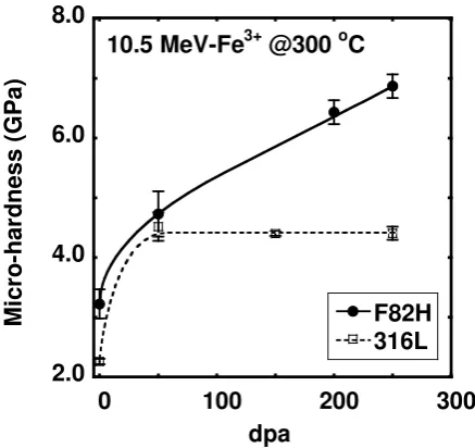
N. Okubo, N. Ishikawa and S. Ohnuki
1-28 Radiation-induced Hardening for SUS316L with Bending Deformation ··· 32
N. Ishikawa, N. Okubo and K. Kondo
1-29 Irradiation Hardening of Extra High Purity Ni-base Superalloy under
External Stress ··· 33
I. Ioka, G. H. Kim and T. Inoue
1-30 Irradiation Hardening of G-Phase Strengthened Ni-base Alloy under
Multi-ion Irradiation ··· 34
N. Okubo, I. Ioka, G. H. Kim and T. Inoue
1-31 Precipitate Stability and Swelling Resistance of High-Nickel Alloy during
Irradiation ··· 35
S. Yamashita, T. Inoue, Y. Sekio, T. Hayashi, I. Yamagata,
T. Yoshitake and T. Kaito
1-32 Effects of Displacement Damage and Gas Atoms on Radiation Hardening and
Microstructure in F82H Weldment ··· 36
M. Ando and H. Tanigawa
1-33 Corrosion Tests of Steels Used for Reactor Pressure Vessel and Primary
Containment Vessel ··· 37
J. Nakano and T. Tsukada
1-34 Corrosion Resistance of Tank Material Used for Flock Storage ··· 38
Y. Sano , H. Ambai, M. Takeuchi and Y. Koma
1-35 Investigation of Microstructure in SiC Made by Nano-infiltration Transient
Eutectic Process after Triple Ion Beam Bombardment ··· 39
K. Ozawa, T. Taguchi T. Nozawa, M. Ando and H. Tanigawa
1-36 Ionizing Dose Dependences of Radiation-induced Conductivity and
Radiation-induced Electrical Degradation of Chemical Vapor Deposited
Silicon Carbides under Gamma-ray Irradiation ··· 40
B. Tsuchiya, T. Shikama, S. Nagata, K. Saito and S. Yamamoto
1-37 Surface Morphology of He Implanted CeO
2Thin Film ··· 41
H. Serizawa, S. Yamamoto and T. Hakoda
1-38 A Macroporous SiC Material Synthesized from Preceramic Polymer with
Direct Foaming and Radiation Curing ··· 42
A. Idesaki, M. Sugimoto and M. Yoshikawa
1-39 Alkaline Durable Anion Exchange Membranes Synthesized by
Radiation-induced Grafting for Hydrazine Hydrate Fuel Cell ··· 43
K. Yoshimura, H. Koshikawa, T. Yamaki, H. Shishitani, S. Yamaguchi,
H. Tanaka and Y. Maekawa
1-40 Preparation of Anion-Exchange Membranes for Fuel Cell Applications by
1-41 Poly(ether ether ketone) (PEEK)-based Graft Type Polymer Electrolyte
Membrane: Relative Humidity Dependence for Fuel Cell Application ··· 45
S. Hasegawa, H. Koshikawa, J. Chen and Y. Maekawa
1-42 Preparation of Novel Polymer Electrolyte Membranes by Combination of
Radiation Induced Grafting and Atom Transfer Radical Polymerization ··· 46
S. Sawada, S. Hasegawa and Y. Maekawa
1-43 Preparation of Platinum Nanoparticle Catalysts for Fuel Cell Applications by
Ion Implantation ··· 47
S. Kato, T. Yamaki, S. Yamamoto, T. Hakoda, K. Kawaguchi, T. Kobayashi,
Y. Maekawa, A. Suzuki and T. Terai
1-44 Ion Content of Ion Exchange Membrane in HI-I
2-H
2O Mixture ··· 48
N. Tanaka, T. Yamaki, M. Asano, T. Terai and K. Onuki
1-45 Applied-Voltage Dependence on Conductometric Track Etching of
Poly(vinylidene fluoride) ··· 49
N. Nuryanthi, T. Yamaki, H. Koshikawa, A. Kitamura (Ogawa), S. Sawada,
M. Asano, S. Hasegawa, Y. Maekawa and Y. Katsumura
1-46 Microscopic Evaluation of the Absolute Fluence Distribution of an Ion Beam
Radiation Tolerance of New Coverglass
for Space Solar Sheet
K. Shimazaki
a), Y. Kobayashi
a), M. Takahashi
a), M. Imaizumi
a),
S. Sato
b)and T. Ohshima
b)a)
Aerospace Research and Development Directorate, JAXA,
b)Environment and Industrial Materials Research Division, QuBS, JAEA
Space solar sheet (SSS) being currently under development is a quite unique and Japan’s original devise for generating electricity in space1). There are two kinds of SSS: one is a film-type SSS using transparent polymer film and the other is glass-type SSS (G-SSS) using a coverglass. Space solar sheet basically possesses 15 paper-like III-V multi-junction solar cells connected in five series and three parallel rows. The cells are laminated with the transparent polymer film or coverglass. To realize G-SSS, features of flexibility, toughness (not crack easily) and high radiation tolerance are inevitably required for the coverglass. Optical degradation of the coverglass caused by space radiation is particularly important since it decreases the amount of transmitted sunlight falling on solar cells and degrades the cell output power. Hence, we evaluated a radiation tolerance of a new coverglass for G-SSS.
Space radiations are omnidirectional charged particles and have energies that range from near-zero up to several hundred million electron volts. However, the present ground tests are different from the actual space radiation environment. Ground tests usually utilize the monoenergetic and normal incident charged particles. For simulating the same level of degradation as the actual space radiation environment, we calculated the energies deposited in the sample using PHITS (Particle and Heavy Ion Transport code System)2,3). The interest sample was a new coverglass with 50 m thickness. Figure 1 illustrates the calculated depth profiles of the deposited energies by space radiations and ground-based monoenergetic irradiations. The assumed space environments and conditions were low-earth orbit for 5 years and geostationary orbit for 10 years. The 1-MeV electron was selected for ground test because its electron completely penetrates the sample. Calculation results show that the required fluences of 1-MeV electron were approximately 2
×
1014 and 2×
1016 e/cm2 for simulating the degradation due to space radiation at Low Earth Orbit (LEO) and Geostationary Orbit (GEO).
Figure 2 depicts the results of irradiation tests. Changes in transmittance due to the irradiations were evaluated as an effective transmittance which corresponded to the relative changes in calculated short-circuit current of the solar cells. The remaining factors of effective transmittance of the coverglass were 98% and 97% at fluences of 2
×
1014 and 2×
1016 e/cm2. The degradation behavior seems to be saturated as the fluence increases. In addition, the coverglass showed same degree of the degradation betweenLEO and GEO conditions although the total dose of GEO was larger than that of LEO by two orders of magnitude. It is expected that the optical properties of the coverglass is stable at different radiation environment. The transmittance loss of the coverglass will be only 3% when it is utilized on geostationary orbit for 10 years. These results demonstrate the developed coverglass exhibit an excellent performance in space and has a high potential for applying to G-SSS.
References
1) T. Takamoto et al., Proc. 35th IEEE PVSC (2010) 412-7.
2) H. Iwase et al., J. Nucl. Sci. Technol. 39 (2002) 1142. 3) K. Niita et al., Radiat. Meas. 41 (2006) 1080.
1 - 01
Fig. 1 Calculated depth profiles of deposited energies in coverglass.
Proton Induced Degradation of Triple Junction
Amorphous Silicon Thin Film Solar Cells
S. Sato and T. Ohshima
Environment and Industrial Materials Research Division, QuBS, JAEA
I. Introduction
Amorphous silicon (a-Si) thin film solar cells are one of the major candidates for flexible space solar cells, since it is known they have not only good radiation tolerance, but also many distinct advantages: high specific power, high
flexibility, ruggedness, and tight rollup feature for stowage1).
Additionally, they also have the potential for reductions of both cost and stowage volume. Recently, the specific power of 1200 W/kg has been attained by triple-junction (TJ) amorphous silicon alloy solar cells using roll-to-roll
processing2). However, systematic knowledge of the
radiation degradation of a-Si solar cells is still insufficient compared to other types of solar cells, such as crystalline Si and III-V compounds.
II. Experimental
Samples used in this study were a-Si/a-Si0.8Ge0.2/
a-Si0.6Ge0.4 TJ solar cells. Proton irradiation was
performed at TIARA. Current-voltage (I-V) characteristics
under air mass zero (AM0), 1 sun light illumination were
measured in-situ in an irradiation chamber. In this study,
proton beam flux, temperature during irradiation, and elapsed time between irradiation and measurement were carefully controlled in order to compare the degradation behavior accurately. The proton beam flux and the
irradiation temperature were 1.4
×
1010 cm-2s-1 and 298 K,respectively, and the I-V measurement was done 1 minute
after irradiation was stopped. The cells were kept under
dark conditions except when the I-V measurement was
performed.
III. Results and Discussion
Figure 1 shows short-circuit current (Isc) variations of the cells as a function of proton fluence (degradation curve). The degradation of Isc was larger as the proton energy was lower, except the results of 10 keV and 20 keV proton irradiations. Protons with energies of 10 keV and 20 keV
stop in the top (a-Si) and middle (a-Si0.8Ge0.2) subcells
respectively and deposit all of their energies in the cell. However, their proton energy itself was less than 40 keV and thus, their induced damage was also lower.
Figure 2 shows the degradation curves of Isc which are scaled using the displacement damage dose (DDD). DDD
is defined as the product of NIEL3) (Non-Ionizing Energy
Loss, MeV·cm2/g) and the proton fluence. In order to
consider the deposited energy distribution as a function of depth in the device structure, NIEL per unit depth was calculated using TRIM code and the average value in the
whole region of the cell was used.
The result clearly show
that a universal curve is drawn using DDD scaling, indicating that the degradation is mainly attributed to the displacement damage effect, which is the same mechanism as the degradation of crystalline silicon solar cells and is very different from the light-induced degradation so
commonly occurring in a-Si solar cells4).
We would like to thank Dr. Kevin Beernink of United Solar Ovonic LLC for fabricating the samples.
References
Fig. 2 Displacement damage dose (DDD) scaling for the degradation curves of Isc.
0 1010
Fig. 1 Degradation of Isc due to proton irradiation. The ordinate axis is normalized by the value before irradiation.
Applicability of the Improved Radiation Hardness
Techniques for Angle Irradiation in DICE Latches on a
65 nm Bulk CMOS Process
A. Maru
a), H. Shindou
a), S. Kuboyama
a), T. Tamura
a), H. Abe
b)and T. Ohshima
b)a)
Aerospace Research and Development Directorate, Japan Aerospace Exploration Agency (JAXA),
b)Environment and Industrial Materials Research Division, QuBS, JAEA
Recently, due to the requirements for higher density integration and device scaling, logical circuits have been fabricated with the process technologies less than 100 nm. Single-Event Upset (SEU) and Single-Event Transient (SET) phenomena are considered serious problems for those integrated circuits, because their supply voltage and the threshold to the phenomena are also decreasing. It was reported that Dual Interlocked Storage Cell (DICE) circuit is the hardened topology against SEU1),2). The DICE circuit keeps data using two memory nodes, and if data inversion occurs by incident particles on the one hand memory node, the correct data is rewritten by the other hand memory node. Therefore, DICE circuit has excellent radiation tolerance. However, in highly integrated circuits, it was found that two neighboring transistors were simultaneously inverted by an incident particle due to the charge sharing mechanism3). Therefore, it is important for the design of highly integrated DICE circuits used in space to estimate the extent of the charge sharing.
In the past study4), we evaluated the effectiveness of the Radiation Hardness By Design (RHBD) approach for 90 nm CMOS process, by using heavy ions from AVF cyclotron at JAEA. The DICE memory test circuit was fabricated by using 90 nm bulk CMOS process and the angled irradiation testing was performed with this circuit. As a result, SEUs were observed in the DICE memory circuit when heavy ions were irradiated with grazing angles. This result can be explained by the simultaneous inversion of a critical transistor pair which triggers SEU in the DICE memory. Due to the penetration of a single heavy ion into the critical transistor pair, SEUs were observed in the previous experiments. To mitigate this, we proposed three node DICE circuits. Figure 1 shows a schematic diagram of our
designed three node DICE circuit. Extra p-type transistors were inserted to the normal DICE circuit. In addition, the critical three transistors were arranged so as not to align in a straight line, and thus, a single ion could not penetrate these critical transistors in this circuit, simultaneously.
In the latest study, we applied this technique to the 65 nm bulk CMOS process and designed the three node DICE circuits. The layout designing indicates an advantage of the circuits area compared with the same circuits on the 90 nm bulk CMOS process: Higher integrated devices used for space are expected to be fabricated by using the 65 nm CMOS process. Table 1 shows a comparison of the circuit area.
The test samples, which were fabricated by using Taiwan Semiconductor Manufacturing Company (TSMC), were evaluated by using heavy ions with LET of 3.4 ~ 68.8 MeV/(mg/cm2). The results indicated that the test circuits exhibited almost the same single event tolerance compared to the circuits fabricated on the 90 nm bulk CMOS process. Therefore, the 65 nm bulk CMOS process is found to be applied to the devices used for space. However, some SEUs were still observed in the three node DICE circuit. There is the possibility to improve SEU tolerance by modifying transistor layout. We continue evaluating newly developed DICE circuits, and will modify the transistor layout in next stage.
References
Fig. 1 Schematic diagram of three node DICE memory cell.
Table 1 Comparison of the circuit area for the conventional DICE and the three node DICE circuits.
Circuit name 90 nm 65 nm
DICE 53.40[um2] 19.44[um2] Three node DICE 70.71[um2] 46.08[um2]
Influence of Generated Charge by High Energy Ion
Irradiation on Soft Error Rate in SOI SRAM
M. Hazama
a), S. Abo
a), F. Wakaya
a), T. Makino
b), S. Onoda
b), T. Ohshima
b),
T. Iwamatsu
c), H. Oda
c)and M. Takai
a)a)
Center for Quantum Science and Technology under Extreme Conditions, Osaka University,
b)Environment and Industrial Materials Research Division, QuBS, JAEA,
c)
Renesas Electronics Corporation
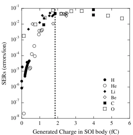
When a semiconductor device is irradiated with a high energy particle, originated from a cosmic ray, electron-hole pairs are generated along its track due to energy consumption of the particle and flow to the circuit, resulting in a soft error. In recent years, a size of a semiconductor device is shrunk for low power consumption and high speed operation. Therefore the amount of charge which induces soft errors (critical charge) for an advanced device has decreased as compared with that for a conventional device. A silicon-on-insulator (SOI) device can suppress the soft errors. Because an active region of the SOI device is separated from a substrate by a buried oxide (BOX) layer, the small amount of charge is generated by the high energy particle in the active region of the SOI device. However the soft errors occur by a floating body effect in the partially depleted (PD) SOI device with the electrically floated active region from the substrate, even if the amount of the generated charge in the SOI body is less than the critical charge. When the electron-hole pairs are generated in the SOI body of an n-channel Metal-Oxide-Semiconductor Field-Effect Transistor (MOSFET), the generated electrons move to the source and drain electrodes and the generated holes move to the neutral region at the bottom of the SOI body. The accumulated holes at the neutral region increase the body potential of the SOI MOSFET, resulting in the abnormal drain current and the soft error. The body-tie structure was invented to suppress the floating body effect, in which the highly doped p-type region is fabricated at the bottom side of the active region of the n-channel SOI MOSFET and connects to the ground potential. The accumulated holes can be retrieved through the highly doped p-type region and the body electrode. In this study, the influence of the amount of the generated charge on the soft error rates (SERs) in the body-tie SOI Static Random Access Memories (SRAMs) are investigated by various ion probes to clarify the effect of the floating body on the soft error.
In order to generate the various amounts of charge, the SOI SRAM with body-tie structure was irradiated with H, He, Li, Be, C, and O, accelerated up to a few tens of MeV by the tandem accelerator. The thicknesses of SOI and BOX layers are 75 nm and 145 nm, respectively. The critical charge of the experimental PD SOI SRAM with a technology node of 90 nm was 1.8 fC. The number of the incident particles to SOI SRAM is counted by a solid state detector (SSD) before and after ion irradiation. The less number of particles than the number of SRAM cells were
used to avoid multi hits to the single SRAM cell. The
generated charge in the SOI layer was calculated byThe
Stopping and Range of Ions in Matter (SRIM) simulator1).
Figure 1 shows SERs as a function of the generated charge in the SOI body by H, He, Li, Be, C and O ion probes. SERs in the SOI SRAM increased with increasing the amount of generated charge below the critical charge. These errors were induced by the floating body effect. SERs which occurred at the amount of the generated charge exceeds the critical charge were almost constant. These errors were induced by the flowed charge and the floating body effect.
The amount of generated charge in the SOI body depends on the kind and energy of the incident particles. Therefore, it is necessary to make measures according to the expected incident particles for realizing the soft-error-free PD SOI devices.
Reference
1) J. Ziegler, The Stopping and Range of Ions in Matter (SRIM2008) <http://www.srim.org>.
Generated Charge in SOI body (fC)
Fig. 1 SERs as a function of amount of the generated charge in the SOI body by using H, He, Li, Be, C and O ion probes for 90 nm node PD SOI-SRAM. The vertical dotted line shows the critical charge of 1.8 fC.
Radiation Damage in Si
1-xGe
xSource/Drain p-type
MOSFETs
K. Takakura
a), I. Tsunoda
a), M. Yoneoka
a), T. Nakashima
b,c)and M. Sugiyama
d) a)Kumamoto National College of Technology,
b)University of Miyazaki,
c)
Chuo Denshi Kogyo Co. Ltd.,
d)Tokyo University of Science
The development of semiconductor devices, which can operate in a radiation-harsh environment, is extensively taking place in a global context. This has been driven by multiple factors, including the high-energy particle accelerators and artificial satellites. Moreover, in the frame of high mobility substrates, new channel materials and/or promising methods to create strained channels are
required1,2). In line with this, we have investigated the
degradation of the device performances of Si1-xGex S/D
(source/drain) p-channel metal oxide semiconductor field effect transistors (p-MOSFETs) irradiated electrons. The purpose of this study is to investigate Ge content
dependence on radiation damage of Si1-xGex S/D
p-MOSFETs.
Si1-xGex (x=0, 0.3 and 0.35) S/D p-MOSFETs were
fabricated at interuniversity microelectronics center (imec)
at Belgium. The Si1-xGex S/D region depth of x = 0.3 and
0.35 samples is 40 nm, and gate length and gate width of all
samples are 0.25 µm and 10 µm. Subsequently, these were
irradiated by 2-MeV electrons for a fluence of 1
×
1017 and5
×
1017 e/cm2 at room temperature, using the electronaccelerator at Takasaki Advanced Radiation Research Institute, JAEA. Before and after electron irradiation,
input (IDS-VGS) characteristic was measured with a drain
voltage at -25 mV and gate voltages ranging from -1.2 to
0.5 V, enabling to estimate the hole-mobility3).
Before irradiation, the drain current increases with increasing Ge content. After irradiation, the drain current decreases with increasing electron fluence for all Ge content. Figure 1 shows the Ge content dependence of the maximum
hole mobility before and after electron irradiation. The hole mobility enhancement effect by SiGe stressor is clearly
observed by x=0.3 and 0.35 samples before irradiation.
These results indicate that the change of the drain current with Ge content can be mainly attributed to the increase of the hole mobility due to the compressive strain in the Si-channel. After electron irradiation, the hole mobility decreases with increasing electron fluence for all Ge content. This result suggests that the lattice defects are introduced by electron irradiation in the Si channel.
The damage factor of maximum hole mobility (DF = µ max-after/µ max-before; where µ max-before and µ max-after are
the maximum hole mobility in before and after electron irradiation) was summarized in Fig. 2 as a function of the Ge content. The damage factor decreases with increasing electron fluence for all Ge content. Moreover, Ge content dependence in the damage factor does not observed. It also indicates that the degradation of hole mobility by electron irradiation does not corresponds to compressive strain in the channel.
References
1) M. Kodera et al., Jpn. J. Appl. Phys. 47 (2008) 2506.
2) K. Rim et al., IEEE IEDM Tech. Dig. (1995) 517.
3) T. Nakashima et al., Thin Solid Films 520 [8] (2012)
3337.
Acknowledgement
Part of this work was supported by Inter-University Laboratory for the Joint Use of JAEA Facilities.
Fig. 1 Hole-mobility before and after electron irradiated
Si1-xGex-S/D p- MOSFETs as a function of the Ge
content.
Fig. 2 The damage factor of electron irradiated
Si1-xGex-S/D p- MOSFETs as a function of the Ge
content.
Anomalous Charge Collection from 4H-SiC Schottky
Barrier Diodes
T. Makino
a), M. Deki
b), N. Iwamoto
a), S. Onoda
a), N. Hoshino
c),
H. Tsuchida
c)and T. Ohshima
a)a)
Environment and Industrial Materials Research Division, QuBS, JAEA,
b)The University of Tokushima,
c)
Central Research Institute of Electric Power Industry (CRIEPI)
Silicon carbide (SiC) are regarded as a promising candidate for a material of electronic devices requiring high radiation tolerance (rad-hard devices). Some results indicate that electronic devices fabricated with SiC have a superior radiation tolerance from the point of view of Total
Ionizing Dose effects (TIDs)1-3). For the development of
rad-hard SiC devices, it is necessary to understand the response of their performance when dense charge is generated in them by an incident ion, resulting in Single Event Effects (SEEs). Silicon carbide can endure an electric field about eight times greater than silicon or GaAs before exhibiting avalanche breakdown. High breakdown electric fields allow for very high-voltage, high-power devices. Permanent malfunctions can be induced in power devices by SEEs, and the probability of SEEs increases with increasing electric field in the device. Since the electric field in SiC power devices must be higher than in Si power devices, it is very important to elaborate the SEEs in SiC devices. Recently, several Schottky Barrier Diodes (SBDs) have become commercially available due to the improvement in crystalline quality. At present, experimental data for understanding the exact mechanisms of SEEs in SiC-SBDs are very scarce and Single Event Burnout (SEB) mechanisms of SiC-SBDs have not been fully understood.
In this study, heavy-ion induced charge collection is demonstrated for thick epi-layer. To reveal SEB mechanisms, the applied bias dependence of the charge collection in SiC-SBDs has been investigated here.
SiC-SBDs used in this study were fabricated on an n-type
4H-SiC epi-layer. The thickness of the epi-layer is 30 µm.
A molybdenum (Mo) contact with a thickness of 50 nm was used as the anode of SiC-SBD. The bonding pad on the
Mo-contact was made of Al (2 µm thick). The bonding
pad area is 1 mm2. We measured the collected charge
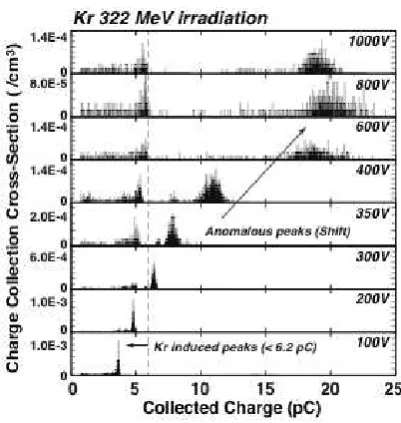
induced by heavy ions in SiC-SBD from its cathode. SiC-SBD was mounted on a chip carrier with two strip-lines with short bonding wires. The anode was grounded and the cathode biased from +100 V to +1,000 V with 50 V to 200 V steps by a high-voltage supply via a charge-sensitive preamplifier (ORTEC Model 142C). Collected charge signals from the pre-amplifier were analyzed by a Pulse-Height Analyzer (PHA). The pulse-height distribution analyzed by PHA basically corresponds to the collected charge distribution.
Figure 1 shows the collected charge spectra from SiC-SBD at different bias conditions. The vertical axes are ion induced pulse generation cross-section. The horizontal axis corresponds to the collected charge. Normally the collected charge spectrum might have a mono-peak similar to that found in a Si-SSD spectrum. In fact, an ion-induced
mono-peak in SiC-SBD was observed in a previous study4).
However, here two major peaks under bias conditions higher than 300 V are observed as shown in Fig. 1. The first peak exists at a value of 6.2 pC in every bias condition. The first peak increases with the reverse bias applied to the cathode, and finally saturates, because the depletion width in the epi-layer increases with the reverse bias and finally saturates. The upper limit of the first peak (6.2 pC) corresponds to the fully-stopped 300 MeV of Kr ion induced charge in 4H-SiC. Here, the mean electron-hole pair creation energy is 7.8 eV in 4H-SiC, while the second peaks are observed as anomalous charge collection beyond 6.2 pC.
Anomalous collected charge peaks (2nd peaks) has been
observed for the first time5). Previous results suggest that the
high electric-field induced by incident ion on SiC-SBD may be a possible reason for the charge enhancement. The higher electric-field may enhance the ion-induced charge due to impact ionization and/or the trap assisted tunneling. However, from these results, we cannot identify the mechanisms of the anomalous charge collection. Therefore, more studies are needed in order to reveal the effective parameter for the anomalous charge collection on SiC-SBD, since an increase of the collected charge may trigger SEB in any devices whatever the charge collection mechanism.
References
Fig. 1 Collected charge spectra from the SiC-SBD5).
![Fig. 2 Change in dissolved oxygen concentration with irradiation time at 1 kGy/h. Initial [N2H4] = 32 ppm](https://thumb-ap.123doks.com/thumbv2/123dok/3991522.1934942/37.595.328.489.537.697/fig-change-dissolved-oxygen-concentration-irradiation-time-initial.webp)