Modelling of DC-DC converters
Ovidiu Aurel Pop and Serban Lungu
X
Modelling of DC-DC converters
Ovidiu Aurel Pop and Serban Lungu
Technical University of Cluj-Napoca
Romania
1. Introduction
The DC-DC converters are electrical circuits that transfer the energy from a DC voltage source to a load and regulate the output voltage. The energy is transferred via electronic switches, made with transistors and diodes, to an output filter and than is transferred to the load.
DC-DC converters are used to convert unregulated dc voltage to regulated or variable dc voltage at the output. They are widely used in switch-mode dc power supplies and in dc motor drive applications. In dc motor control applications, they are called chopper-controlled drives. The input voltage source is usually a battery or derived from an ac power supply using a diode bridge rectifier. These converters are generally either hard-switched PWM types or soft-switched resonant-link types.
These converters employ square-wave pulse width modulation to achieve voltage regulation. The output voltage is regulated varying the duty cycle of the power semiconductor switch driving signal. The voltage waveform across the switch and at the input of the filter is square wave in nature and they generally result in higher switching losses when the switching frequency is increased. Also, the switching stresses are high with the generation of large electromagnetic interference (EMI), which is difficult to filter. However, these converters are easy to control, well understood, and have wide load control range.
These converters operate with a fixed-frequency, variable duty cycle. This type of signal is called Pulse Width Modulated signal (PWM). Depending on the duty cycle, they can operate in either continuous current mode (CCM) or discontinuous current mode (DCM). If the current through the output inductor never reaches zero then the converter operates in CCM; otherwise DCM occurs.
The output voltage will be equal with the average value on the switching cycle of the voltage applied at the output filter. Due to the losses on the ON or OFF state of the ideal transistor are zero, the theoretical efficiency of the switching mode converters is up to 100%. But, considering the real switches, with parasitic elements, the efficiency will be a little bit lower, but higher than linear regulators.
Another advantage of switching mode converters consist in the possibility to use the same components but in other topology in order to obtain different values of the output voltages: positive or negative, lower or higher than input voltage.
There are various analysis methods of DC-DC converters. Throughout the chapter an extended analysis and modelling for DC-DC power converters is proposed. In this approach, the differential equations that describe the inductor current and capacitor voltage are determined and are solved according with the boundary conditions of the switching periods. The values of currents and voltages at the end of a period become initial conditions for the next switching period. This method is very accurate and produces a set of equations that require extensive computation.
In addition, for specified values of converter parameters (inductance and capacitor) we can calculate the maximum value of transistor and diode current and reverse voltage, in order to help user to choose the appropriate type of transistor and diode.
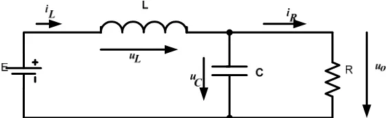
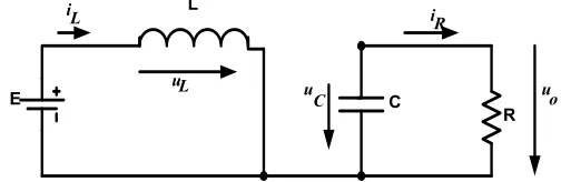
2. Buck converter
The buck (or step-down converter), shown in the figure 1, contain a capacitor and an inductor with role of energy storing, and two complementary switches: when one switch is closed, the other is open and vice-versa.
Fig. 1. The buck converter diagram
The switches are alternately opened and closed with at a rate of PWM switching frequency. The output that results is a regulated voltage of smaller magnitude than input voltage. The converter operation will be analyzed function of switches states.
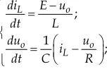
The first time interval: The transistor is in ON state and diode is OFF.
During this time period, corresponding with duty cycle of PWM driving signal, the equivalent diagram of the circuit is presented bellow:
Fig. 2. The equivalent circuit during the ON state of transistor and OFF state of diode
For this equivalent circuit will write the equations that describe the converter operation:
1
( ) ;
;
o o
L
L o
du i u
dt R C
di E u
dt L
(1)
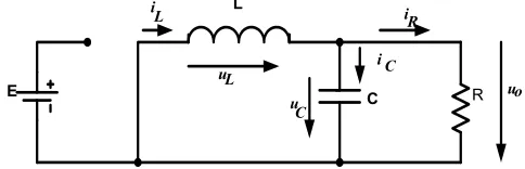
The second time period: the transistor is OFF and diode is ON
In the moment when the transistor switch in OFF state, the voltage across the inductor will change the polarity and the diode will switch in ON state. The equivalent diagram of converter during this period is shown in the bellow figure:
E
L
C R
i
u L
C L
u uo
iR i C
Fig. 3. The equivalent circuit for OFF state of transistor and ON state of diode
For this operation period, the output voltage u0 and the current through the inductor iL
satisfy the following equations:
1 ;
;
o o
L
L o
du i u
dt R C
di u
dt L
(2)
The third operation mode: The both transistor and diode are OFF
If the inductor current becomes zero before ending the diode ON period, both transistor and diode will naturally closed. This operation regime is called discontinuous current mode. The equivalent diagram of this operation regime is shown bellow.
E
L
C R
u
C L
u uo
iR i C
There are various analysis methods of DC-DC converters. Throughout the chapter an extended analysis and modelling for DC-DC power converters is proposed. In this approach, the differential equations that describe the inductor current and capacitor voltage are determined and are solved according with the boundary conditions of the switching periods. The values of currents and voltages at the end of a period become initial conditions for the next switching period. This method is very accurate and produces a set of equations that require extensive computation.
In addition, for specified values of converter parameters (inductance and capacitor) we can calculate the maximum value of transistor and diode current and reverse voltage, in order to help user to choose the appropriate type of transistor and diode.
2. Buck converter
The buck (or step-down converter), shown in the figure 1, contain a capacitor and an inductor with role of energy storing, and two complementary switches: when one switch is closed, the other is open and vice-versa.
Fig. 1. The buck converter diagram
The switches are alternately opened and closed with at a rate of PWM switching frequency. The output that results is a regulated voltage of smaller magnitude than input voltage. The converter operation will be analyzed function of switches states.
The first time interval: The transistor is in ON state and diode is OFF.
During this time period, corresponding with duty cycle of PWM driving signal, the equivalent diagram of the circuit is presented bellow:
Fig. 2. The equivalent circuit during the ON state of transistor and OFF state of diode
For this equivalent circuit will write the equations that describe the converter operation:
1
( ) ;
;
o o
L
L o
du i u
dt R C
di E u
dt L
(1)
The second time period: the transistor is OFF and diode is ON
In the moment when the transistor switch in OFF state, the voltage across the inductor will change the polarity and the diode will switch in ON state. The equivalent diagram of converter during this period is shown in the bellow figure:
E
L
C R
i
u L
C L
u uo
iR i C
Fig. 3. The equivalent circuit for OFF state of transistor and ON state of diode
For this operation period, the output voltage u0and the current through the inductor iL
satisfy the following equations:
1 ;
;
o o
L
L o
du i u
dt R C
di u
dt L
(2)
The third operation mode: The both transistor and diode are OFF
If the inductor current becomes zero before ending the diode ON period, both transistor and diode will naturally closed. This operation regime is called discontinuous current mode. The equivalent diagram of this operation regime is shown bellow.
E
L
C R
u
C L
u uo
iR i C
For this operation period, the output voltage uo and the current through the inductor iL
satisfy the following equations:
1 ;
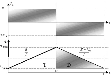
2.1 CCM inductance
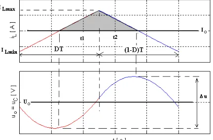
The minimum value of inductance for continuous current mode (CCM) operation is calculated from output voltage and inductor current equations.
Thus, the output voltage uoand the current through the inductor iL satisfies the following
equations:
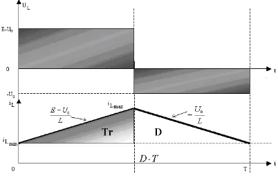
Fig. 5. The waveforms of output voltage and inductor current
In the steady state regime, the average value of voltage across the inductor is zero. Thus,
EUo
DTUoT
1D
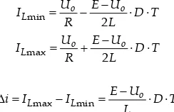
UoDE (6)Based on the inductor current waveform, the following equation can be write:
max min
The average value of the inductor current is equal with the output current:
max min
From the equations (6) and (11) the inductor current ripple can be calculated.
T switching frequency and load value are known.
D
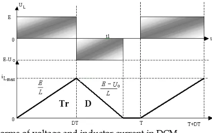
2.2 The discontinuous current mode
In discontinuous current regime, the waveforms of inductor voltage and current are shown in the figure bellow:
For this operation period, the output voltage uo and the current through the inductor iL
satisfy the following equations:
1 ;
2.1 CCM inductance
The minimum value of inductance for continuous current mode (CCM) operation is calculated from output voltage and inductor current equations.
Thus, the output voltage uoand the current through the inductor iL satisfies the following
equations:
Fig. 5. The waveforms of output voltage and inductor current
In the steady state regime, the average value of voltage across the inductor is zero. Thus,
EUo
DTUoT
1D
UoDE (6)Based on the inductor current waveform, the following equation can be write:
max min
The average value of the inductor current is equal with the output current:
max min
From the equations (6) and (11) the inductor current ripple can be calculated.
T switching frequency and load value are known.
D
2.2 The discontinuous current mode
In discontinuous current regime, the waveforms of inductor voltage and current are shown in the figure bellow:
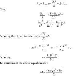
The average value of the input current is equal with the current through the switching
From the above equations, it results:
2
Denoting the circuit transfer ratio
E
the solutions of the above equation are:2 4 2
a a a
M . (23)
Analyzing those solutions, can be observed that the single valid solution is
2 4 2
a a a
M (24)
The variation of circuit transfer ratio M function of PWM signal duty-cycle D, for different
values of
2
L
RT
parameters is shown in the figure:Fig. 7. Variation of circuit transfer ratio M function of PWM signal duty-cycle D
2.3 Filtering capacitor
Other important parameter that is important to be determined is the value of the output capacitor, in order to obtain a specific value of the output voltage ripple.
The capacitor charging current is equal with difference between the inductor current iL and
the output current iO. Considering a constant output current, the electric charge stored in the
capacitor during a switching period is equal with the shade area from the figure bellow:
Fig. 8. The waveforms of inductor current and output voltage
Thus, the value of the output capacitor can be calculated with the following formula:
It can be seen in this formula that the capacitor value depends by the switching frequency. Increasing the switching frequency, the capacitor value will be smaller.
3. Boost Converter
The boost (or step-up converter), shown in the figure 9, contains, like the Buck converter, a capacitor and an inductor with role of energy storing, and two complementary switches. In the case of the boost converter, the output voltage is higher than the input voltage.
Fig. 9. The boost converter diagram
The switches are alternately opened and closed with at a rate of PWM switching frequency. As long as transistor is ON, the diode is OFF, being reversed biased. The input voltage, applied directly to inductance L, determines a linear rising current. When transistor is OFF, the load is supplied by both input source and LC filter. The output that results is a regulated voltage of higher magnitude than input voltage. The converter operation will be analyzed according with the switches states.
The first time interval: The transistor is in ON state and diode is OFF.
During this time period, corresponding with duty cycle of PWM driving signal, the equivalent diagram of the circuit is presented bellow. In this time period the inductance L store energy.
Fig. 10. The equivalent circuit during the ON state of transistor and OFF state of diode
For this operation period, the output voltage uo and the current through the inductor iL
satisfies the following equations:
;
The second time period: the transistor is OFF and diode is ON
In the moment when the transistor switch in OFF state, the voltage across the inductor will change the polarity and diode will switch in ON state. The equivalent diagram of converter during this period is shown in the bellow figure:
Fig. 11. The equivalent circuit for OFF state of transistor and ON state of diode
For this operation period, the output voltage uo and the current through the inductor iL
satisfy the following equations:
;
The third operation mode: The both transistor and diode are OFF
If the inductor current becomes zero before ending the diode conduction period, both the transistor and the diode will be in OFF state. Due to the diode current becomes zero, the diode will naturally close, and the output capacitor will discharge on the load. This operation regime is called discontinuous current mode. The equivalent diagram of this operation regime is shown bellow.
E
For this operation period, the output voltage uoand the current through the inductor iL can
be calculated from the following equations:
0;
3.1 CCM inductance
The minimum value of inductance for continuous current mode (CCM) operation is calculated from inductor current equation. In the steady state regime, the average value of voltage across the inductor is zero.
Fig. 13. The waveforms of inductor voltage and current in steady-state regime
Thus, the output voltage u0and the current through the inductor iL satisfies the following
equations:
Based on the above waveforms, the maximum value of the inductor current is:
T
The output current is equal with the diode average current:
Based on the equations (32) and (33), results:
Based on the equations (34) and (35), can be determined the inductor current ripple: E D T
i L
(36)
From the condition for continuous conduction mode, iLmin 0, results:
22L D 1 D
R T (37)
This condition can be used to determine the minimum inductance value, for a specific switching period T and a specific load value R.
2 min R T2 1L D D (38)
3.2 The discontinuous current mode
In discontinuous conduction mode, the waveforms of the inductor voltage and current are shown in the figure bellow:
Fig. 14. The waveforms of voltage and inductor current in DCM
The average value of the input current is equal with the inductor average current.
1
Based on the equations (39) and (40), results:
The average value of the inductor voltage during a switching period is zero.
Replacing equation (42) in the equation (41), and also considering the input and the output power equals,
Denoting the voltage transfer ratio with M= E
Uo, the equation (44) becomes:
1
2The solution of this equation is:
2
The variation of circuit transfer ratio M function of PWM signal duty-cycle D, for different values of 2L
RTparameters is shown in the figure:
Fig. 15. Variation of circuit transfer ratio M function of PWM signal duty-cycle D
3.3 Filtering capacitor
Other important parameter that is important to be determined is the value of the output capacitor, in order to obtain a specific value of the output voltage ripple.
The capacitor charging current is equal with the difference between the diode current iD and
the output current io. Considering a constant output current, the electric charge stored in the
capacitor during a switching period is equal with the shade area from the figure bellow:
Fig. 16. The waveforms of inductor current and output voltage
max 2
Thus, the value of the output capacitor can be calculated with the following formula:
4. Buck-Boost converter
The buck-boost converter (polarity inverter) is shown in figure 17.
The switches are alternately opened and closed with at a rate of PWM switching frequency. As long as the transistor is ON, the diode is OFF, being reversed biased. The input voltage, applied directly to inductance L, determines a linear rising current. The capacitor is discharged on the load circuit. When the transistor is OFF, the load is supplied by LC filter. The output that results is a regulated voltage of smaller or higher magnitude than input voltage, depending on the value of duty cycle, but it has a reverse polarity. The converter operation will be analyzed according with the ON or OFF state of switches.
The first time interval: The transistor is in ON state and diode is OFF.
During this time period, corresponding with duty cycle of PWM driving signal, the equivalent diagram of the circuit is presented bellow. In this time period the inductance L stores energy. The load current is assured by the output capacitor.
Fig. 18. The equivalent circuit during the ON state of transistor and OFF state of diode
For this operation period, the output voltage uoand the current through the inductor iL are
given by the following equations system:
L
o o
di E dt du u
dt R C
(50)
The second time period: the transistor is OFF and diode is ON
In the moment when the transistor switch in OFF state, the voltage across the inductor will change the polarity and diode will switch in ON state. The energy stored in the inductor will supply the load. The equivalent diagram of converter during this period is shown in the figure bellow:
Fig. 19. The equivalent circuit during the OFF state of transistor and ON state of diode
For this operation period, the following equations for the output voltage uoand the current
through the inductor iL can be written:
1 L o
o o
L
di u dt L du i u
dt R C
(51)
The third operation mode : The both transistor and diode are OFF
If the inductor current becomes zero before ending the diode ON period, both the transistor and the diode will be OFF. Due to the diode current becomes zero, the diode will naturally close, and the output capacitor will discharge on the load. This operation regime is called discontinuous current mode. The equivalent diagram of this operation regime is shown bellow.
Fig. 20. The equivalent diagram for discontinuous conduction mode operation
For this operation mode, the output voltage uoand the current through the inductor iL can be
calculated from the following differential equations:
0
L
o o
di dt
du u
dt R C
(52)
4.1 CCM inductance
Fig. 21. The inductor voltage and current waveforms in steady-state regime
In the steady state regime, the average value of the voltage across the inductor is zero. From this condition, the output voltage Uo can be determined:
Based on the above waveforms:
max min
L L E
I I D T
L
(54)
Also, the average diode current is equal with the output current.
Based on the equations (54) and (55), the maximum and the minimum value of the inductor current will be:
Thus, the inductor current ripple is:
E D T i
L
(58)
From the condition for continuous conduction mode, iLmin 0, results:
22L 1 D
RT (59)
This condition can be used to determine the minimum inductance value, for a specific switching period T and a specific load value R.
2
1 2
min R T D
L (60)
4.2 The discontinuous current mode
In discontinuous conduction mode, the waveforms of the inductor voltage and current are shown in the figure bellow:
Fig. 22. The waveforms of voltage and inductor current in DCM
The average value of the input current is equal with the transistor average current.
max
From the above equations results:
2
Neglecting the losses in the circuit, the input power is equal with the output power.
Denoting the voltage transfer ratio E
Uo=M , it results:
2 R T M D
L
(66)
The variation of circuit transfer ratio M function of PWM signal duty-cycle D, for different values of 2L
RTparameters is shown in the figure:
Fig. 23. Variation of circuit transfer ratio M function of PWM signal duty-cycle D
4.3 Filtering capacitor
Other important parameter that must be determined is the value of the output capacitor, in order to obtain a specific value of the output voltage ripple.
The capacitor charging current is equal with difference between the diode current iD and the
output current io. Considering a constant output current, the electric charge stored in the capacitor during a switching period is equal with the shade area from the bellow figure:
Fig. 24. The waveforms of the inductor current and output voltage
max 2
1 ( )
2 L o
Q C u I I t
(67)
2 max
max min
(1 ) LL Lo
t I I
T D I I
(68)
The value of the output capacitor can be calculated with the following formula:
2 max
max min
(1 ) 2
L o
L L
I I T D
C
I I
(69)
5. Matlab Modeling of DC-DC Converters
In order to simulate the converters, the equations that describe the converter operation on each of the three possible operating stages are implemented in Matlab, and solved using Matlab facilities.
The program structure consists in two files. The first file initializes the default values of converter parameters: the input voltage E, the inductance value L, the capacitor value C, the load value R, the switching period T, the duty-cycle D and the number of periods to be displayed. All the parameters can be changed during the converters simulation. The structure of this file is:
Listing for initialization of default parameters values clear all;
close;
E=10; %input voltage value
L=1e-4; %inductor value
C=10e-6; %capacitor value
R=10; %load value
%---Q=sqrt(L./C)./R; T0=2.*pi.*sqrt(L.*C);
%---T=50e-6; %switching period
D=0.5; %duty-cycle
N=20; %numbers of periods to be displayed
%---p=1; % default plotting regime (transient)
%---type=1; % default analyzed converter -Buck %type=2; % Boost
%type=3; % Buck-Boost
As it can be seen at the end of the file, the ed_converter(E,L,C,R,T,D,N,p,type) function is called. This function is implemented in a file with the same name, and had as arguments the converter parameters. In the first part of the file are created the buttons that allow to change the values of the converter parameters. Than, are implemented the functions that solve the differential equations that describe the converter operation and are calculated the critical values of inductor for continuous conduction mode operation and value of output voltage. Also, are defined the plots for output voltage and input current.
The structure of this file is presented bellow:
Listing of function file
function ed_converter(E,L,C,R,T,D,N,p,type);
%create a new figure;
Fig=figure('Name',' DC-DC Converters',...
'Numbertitle','off', 'color', [1, 1, 1]);
% creating 7 text buttons B_T;
txt=['E [V] L[ H] C[ F] R[ohm] T[ s] D N ']; for k=1:7
B_T(k)=uicontrol('Style','text', ...
'Units','normalized', ...
% Creating 7 Edit buttons B_E ;
var=['E';'L';'C';'R';'T';'D';'N']; val=[E;L;C;R;T;D;N];
xc= '=str2num(get(gco,''String''));close;ed_converter(E,L,C,R,T,D,N,p,type)';
for i=1:7
B_E= uicontrol('Style','edit',...
'Units','normalized',...
%Creating the control buttons for selection of converter type: Buck, Boost or Buck-Boost
Buck=uicontrol('Style','pushbutton',... Buck_Boost=uicontrol('Style','pushbutton',...
'Units','normalized',...
% When a button is pushed, the callback will call again the function file with the newer parameters
%Routine for solving the function ec_conv, that describes the converters operation t=0;
subplot('Position',[0.10 0.55 0.80 0.35]); plot(t,y(:,1),'r');grid on;hold on; subplot('Position',[0.10 0.15 0.80 0.35]); plot(t,y(:,2),'r');grid on;hold on;
%---interval=2;
tf=k.*T; ci=y(nt,:); interval=2;
options=odeset('Events',@conv_ev);
[t,y,te,ye,ie]=ode45(@ec_conv,[t0,tf],[ci],[options],E,R,L,C,type,interval); nt=length(t);
subplot('Position',[0.10 0.55 0.80 0.35]); plot(t,y(:,1),'b');grid on;hold on; subplot('Position',[0.10 0.15 0.80 0.35]); plot(t,y(:,2),'b');grid on;hold on;
%---interval=3;
if te>0; t0=t(nt); tf=k.*T; ci=y(nt,:); interval=3;
[t,y]=ode45(@ec_conv,[t0,tf],[ci],[],E,R,L,C,type,interval);
%---subplot('Position',[0.10 0.55 0.80 0.35]); plot(t,y(:,1),'g');grid on;hold on; subplot('Position',[0.10 0.15 0.80 0.35]); plot(t,y(:,2),'g');grid on;hold on;
%---end
if (p==0)&(j<N-1)
subplot('Position',[0.10 0.55 0.80 0.35]); hold off;
end
if (p==0)&(j<N-1)
subplot('Position',[0.10 0.15 0.80 0.35]); hold off;
end
end
%========================================
subplot('Position',[0.10 0.55 0.80 0.35]); ylabel(['iL [ A ]']);
switch type; case 1
Lm=R.*T.*(1-D)./2; %Calculating the minimum value of inductance for Buck Converter
if 2.*L./(R.*T)>=1-D
Uo=E.*D; %Calculating the output voltage in Continuous conduction mode
else
z=0.5.*R.*D.^2.*T./L; v=0.5.*(sqrt(z.^2+4.*z)-z);
Uo=v.*E; %Calculating the output voltage in Discontinuous conduction mode
end
title(['Buck Converter',' Uo = ',num2str(Uo),' [ V ]',' Lm = ',num2str(Lm),' [ H ]']);
case 2
Lm=R.*T.*D.*(1-D).^2./2; %Calculating the minimum value of inductance for Boost Converter
di=E.*D.*T./L;
if 2.*L./(R.*T)>=D*(1-D).^2
Uo=E./(1-D); %Calculating the output voltage in Continuous conduction mode
else
v=0.5.*(1+sqrt(1+2.*D.^2.*T.*R./L));
Uo=v.*E; %Calculating the output voltage in Discontinuous conduction mode
end
title(['Boost Converter',' Uo = ',num2str(Uo),' [ V ]',' Lm = ',num2str(Lm),' [ H ]']);
case 3
Lm=R.*T.*(1-D).^2./2, %Calculating the minimum value of inductance for Buck-Boost Converter
if 2.*L./(R.*T)>=(1-D).^2
Uo=E.*D./(1-D); %Calculating the output voltage in Continuous conduction mode
else
v=D.*sqrt(0.5.*T.*R./L);
Uo=v.*E; %Calculating the output voltage in Discontinuous conduction mode
end
title(['Buck-Boost Converter',' Uo = ',num2str(Uo),' [ V ]',' Lm = ',num2str(Lm),' [ H ]']);
end
subplot('Position',[0.10 0.15 0.80 0.35]); ylabel(['Uo = uC [ V ]']);
xlabel(['t [ s ]']);
%Function that describes the converters operation
function dy=ec_conv(t,y,E,R,L,C,type,interval); dy=zeros(2,1);
switch type;
case 1
elseif interval==2
function [value,isterminal,direction] =conv_ev(t,y,E,R,L,C,type,interval); value = y(1); % detect iL = 0
isterminal = 1; % stop the integration
direction = -1; % negative direction
As it can be seen in the converters description, for all types of converters, the equation that describes the operation has the same shape. The difference consists in the value of the coefficients. From this reason, the same equations are used for the simulation of the converters operation and from each converter only the value of a, b, and c coefficients are set. The equations system is:
1
The simulation results of the dc-dc converters are presented in the following figure:
0 0.1 0.2 0.3 0.4 0.5 0.6 0.7 0.8 0.9 1
Fig. 25. The converters simulation results
As can be seen in the figure, from the upper left side button can be chosen the display mode: transient, when all the simulated periods are plotted or steady state regime when only the last simulated period is plotted.
From the right site editing buttons, all of the converter parameters can be set. From the bottom side it can be selected the desired converter: buck, boost or buck-boost. Also, for each converter type, the program displays the output voltage value and the minimum inductance value in order to obtain continuous current mode operation.
6. References
Attaway, S (2009). Matlab: A Practical Introduction to Programming and Problem Solving, 480 pages, Butterworth Heinemann, ISBN 978-0-7506-8762-1, USA
Attia, J. (1999). Electronics and Circuits Analysis using Matlab, 378 pages, CRC Press, ISBN 0-8493-1176-4, USA
Erickson, R.W. & Macksimovic, D. (2001). Fundamentals of Power Electronics, Second ed., 920 pages, Kluver Academic Publisher, ISBN 0-7923-7270-0, USA
Mohan, N. & Undeland, T.M. (2003). Power Electronics: Converters, Applications and Design. Third Ed., 802 pages, John Wiley & Sons, ISBN 0-4714-2902-2, USA
Lungu, S. & Pop, O.A. (2006). Modelling of Electronics Circuits, 133 pages, Science Books House, ISBN 978-973-686-975-4, Romania