NUMERICAL CALCULATION OF THE ELECTRON MOBILITY IN
GaAs SEMICONDUCTOR UNDER WEAK ELECTRIC FIELD
APPLICATION
H. Arabshahi, Z. Moodi and A. Pourhasan
Department of Physics, Payame Noor University, P.O. Box 19395-3697, Tehran, Iran Email: [email protected]
Abstract: In this study, electrons mobility of GaAs semiconductor with using the iterative method in the temperature range of 100-600 K at low field range is calculated .We have considered the polar optic phonons, ionized impurity scattering and acoustic phonon scattering mechanisms. Temperature and doping dependencies of electron mobility in GaAs crystal structure have been calculated using an iterative technique. It is found that the electron mobility decreases monotonically as the temperature increases from 100K to 500K which is depended to the band structure characteristics of GaAs. The low temperature value of electron mobility increases significantly with increasing doping concentration.
Keywords: Electron Mobility; Ionized impurity scattering; Polar optic phonons, Doping.
1. Introduction
GaAs is a semiconductor that is used for manufacturing of high-frequency
microwave and Integrated circuits and diodes in the light (LED) and semiconductor laser
diodes, and solar batteries. Knowing the electron transport in this material is important for
In order to better design pieces that are based on a GaAs. This work shows the results of
numerical calculations of the reversible electron transport in the GaAs. High pure GaAs
semiconductor is one of the best semiconductor detectors, which can be made in large size
with a very suitable high energy resolution. Although, high pure GaAs is very costly and
must be kept at low temperature, it is widely used for gamma and x-ray spectroscopy1.
When this crystal is located in a combined neutron-gamma field, neutron interactions with
on the energy, neutron interactions with matter may undergo a variety of nuclear processes.
The main interactions of fast neutrons are elastic scattering and inelastic scattering, but
neutron capture is an important interaction for thermal neutrons3. Improved electron
transport properties are one of the main targets in the ongoing study of semiconductor like
GaAs. The iterative technique has proved valuable for studying non-equilibrium carrier
transport in a range of semiconductor materials and devices. However, carrier transport
modeling of GaAs material has only recently begun to receive sustained attention, now that
the growth of compounds and alloys is able to produce valuable material for the electronics
industry. In this communication we present iterative calculations of electron drift mobility
in low electric field application4. We demonstrate the effect of low electric field on the
electron transport properties in these materials. The differences in transport properties are
analyzed in terms of important material parameters. Most of the calculations have been
carried out using a non-parabolic ellipsoidal valley model to describe transport in the
conduction band. In this calculation we have used the model of non-parabolic ellipsoidal
valley to describe transport in the conduction band.
2. Method
In principle the iterative technique give exact numerical prediction of electron mobility in
bulk semiconductors. To calculate mobility, we have to solve the Boltzmann equation to
get the modified probability distribution function under the action of a steady electric field.
Here, we have adopted the iterative technique for solving the Boltzmann transport
equation. Under application of a uniform electric field the Boltzmann equation can be
written as5
e E f s f f sf f dk
k = − − −
∇ [ ' '(1 ) (1 ')] .
)
( (1)
where f=f(k) and f′=f(k′) are the probability distribution functions and s=s(k,k') and s'=s(k',k)
are the differential scattering rates. If the electric field is small, we can treat the change
from the equilibrium distribution function as a perturbation which is first order in the
electric field. The distribution in the presence of a sufficiently small field can be written
quite generally as
wheref0(k) is the equilibrium distribution function, θ is the angle between k and E and g(k)
is an isotropic function of k, which is proportional to the magnitude of the electric field.
In general, contributions to the differential scattering rates come from two types of
scattering processes, elastic scattering sel, due to acoustic, impurity, plasmon and
piezoelectric phonons, and inelastic scattering sinel, due to polar optic phonons
s(k,k')=sel(k,k')+sinel(k,k') (3)
Generally this scattering process can not be treated within the framework of the relaxation
time approximation because of the possibility of the significant energy exchange between
the electron and the polar optic modes. In this case,sinelrepresents transitions from the state
characterized by k to k' either by emission [sem(k,k')] or by absorption [sab(k,k')] of a phonon.
The total elastic scattering rate will be the sum of all the different scattering rates which are
considered as elastic processes, i.e. acoustic, piezoelectric and ionized impurity. In the case
of polar optic phonon scattering, we have to consider scattering-in rates by phonon
emission and absorption as well as scattering-out rates by phonon absorption and emission.
Using Boltzmann equation and considering all differential scattering rates, the factor g(k)
in the perturbed part of the distribution function f(k) can be given by6
Note, the first term in the denominator is simply the momentum relaxation rate for elastic
scattering. It is interesting to note that if the initial distribution is chosen to be the
equilibrium distribution, for which g(k) is equal zero, we get the relaxation time
approximation result after the first iteration. We have found that convergence can normally
be achieved after only a few iterations for small electric fields. Once g(k) has been
evaluated to the required accuracy, it is possible to calculate quantities such as the drift
3. Discussion of results
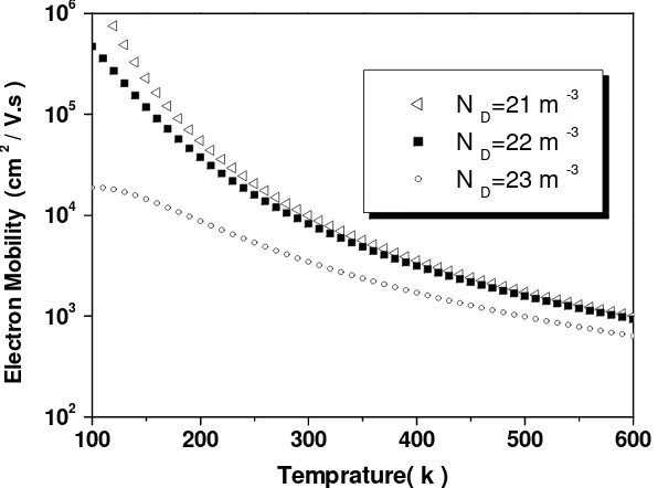
Figure 1 shows the calculated electron drift mobility in bulk GaAs material as a function of
temperature with free electron concentration of 1021 to 1023 m-3 and with the electric field
applied along one of the cubic axes. It can be seen from the figure that the electron drift
mobilities at room temperature that we find for GaAs is 3000 cm2/V-s at 1023 m-3 donor
concentration. The results plotted in figure 1 indicate that the electron drift mobility of
GaAs is lower at donor concentration of 1023 m-3 at all temperatures. This is largely due to
the higher electron scattering rate. Also it can be seen that below 100 K, ionized impurity
scattering is the dominant forms of lattice scattering.
100 200 300 400 500 600
102
Figure 2 shows the piezoelectric scattering rate in term of energy in GaAs for different temperatures. It is observed that with increasing energy of the external electric field the scattering rate is decreased. The piezoelectric scattering process at higher temperatures and low energy electron energy is important
0.0 0.2 0.4 0.6 0.8
Fig 2. Piezoelectric electron scattering rate in terms of energy for different temperature in GaAs.
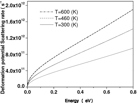
Figure 3 shows the deformation potential electron scattering rate in GaAs at different temperatures. The scattering rate of electrons at higher temperatures is higher also it can be seen that the amplitude of oscillations of atoms increases with increasing temperature
0.0 0.2 0.4 0.6 0.8
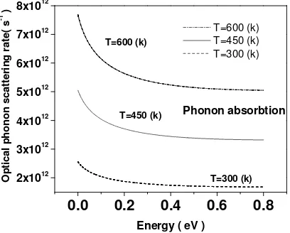
Figures 4 and 5 show the change of polar optical scattering rate in GaAs in the state of absorption and emission. Figure 4 is for the absorption of phonons in terms of electron energy. It can be seen that with increasing the energy, electron scattering does not change. But at higher temperatures it increase.
0.0 0.2 0.4 0.6 0.8
Fig. 4. Electron scattering rate by polar optical phonons of energy at different temperature for absorption of phonons.
0.0 0.2 0.4 0.6 0.8
Fig. 5. Electron scattering rate by polar optical phonons of energy at different temperature for emission of phonons.
primary electron energy of optical phonons in GaAs exceeds 0.35 eV. Then slowly decreases with increasing energy dispersion of the electrons. In this case, higher temperatures are more scattered.
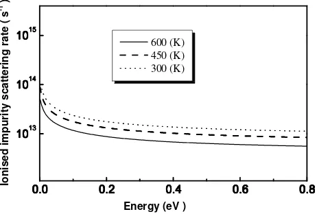
Finally, figure 6 show the ionized impurity scattering rate of electrons in GaAs. It can be seen that at high electric fields the electron scattering from impurity atoms is much higher.
✢✣✢
In conclusion, we have quantitatively obtained temperature-dependent and electron concentration-dependent electron mobility in GaAs using an iterative technique. The theoretical values show good agreement with recently obtained experimental data. Several scattering mechanisms have been included in the calculation. Ionized impurities have been treated beyond the Born approximation using a phase shift analysis. Screening of ionized impurities has been treated more realistically using a multi-ion screening formalism, which is more relevant in the case of highly compensated III-V semiconductors like GaAs.
References
[1] Arabshahi H (2009). Comparison of SiC and ZnO field effect transistors for high power applications, Modern Phys. Lett. B, 23, 2533-2539.
[2] Bertazzi F, Goano M and Bellotti E (2007). Electron and hole transport in bulk ZnO: A full band monte carlo study, J. Elec. Mat. 36, 857-863.
[4] Farahmand M, Garetto C, Bellotti E, Brennan K F, Goano M, Ghillino E, Ghione G, and Ruden P (2001). Monte Carlo simulation of electron transport in the III-nitride wurtzite phase materials system: binaries and ternaries, IEEE Transactions on Electron Devices, 48, 535-539.
[5] Jacoboni C and Lugli P (1989): The Monte Carlo method for semiconductor and device simulation, Springer- Verlag, 3, 221-234.
[6] Moglestue C(1993). Monte Carlo simulation of semiconductor devices, Chapman & Hall, 4, 190-198.