The Deposition of Silver (Ag) On a Glass
Substrate (SiO
2) Using Direct Current
Sputtering Method
Leni Rumiyanti
1, a *, Erika Sempana Br Ginting
2,b, Ihwanul Aziz
3,c,
Simon Sembiring
4,dand Warsito
5,e1Department of Physics, FMNS, University of Lampung, Lampung, Indonesia 2Department of Physics, FMNS, University of Lampung, Lampung, Indonesia 3Center Science and Accelerator Technology, BATAN, Yogyakarta, Indonesia 4Department of Physics, FMNS, University of Lampung, Lampung, Indonesia 5Department of Physics, FMNS, University of Lampung, Lampung, Indonesia
a[email protected], b[email protected], c[email protected], d[email protected], e[email protected]
Abstract
The research's aims are to calculate the absorbance and the thickness value of the silver (Ag) thin layer formed on the glass substrate (SiO2) at various visible wavelengths.
The silver (Ag) thin layer was formed using Direct Current Sputtering method. The research showed that the highest absorbance value on the glass (SiO2) substrate was
4.000 with wavelengths 287.50 nm. While, the lowest absorbance value on the glass (SiO2) substrate was -4.000 with wavelengths 262.50 nm and 243 nm. The lowest
absorbance value is estimated because of the part of the substrate that has not been completely coated so that the part is not absorbed at all. Using Swanepoel equation we obtained the thickness value of the thin layer equal to 4.692663316 nm with sputtering time of 15 minutes.
Keywords:
Direct Current Sputtering, thin layer, silver1. Introduction
A thin layer or film is one of the many materials that called as nanomaterial. The thickness of a thin layer or film are usually between 10-6 m to 10-9 m [1]. It needs
DC Sputtering used an ionization process to release target's atoms onto a substrate material. A sputtering system could layer all kinds of metal, metal alloy or non-metal onto a substrate material [4]. Argon gas was use to sputter or deposition a target material onto the surface of substrate material. Argon was used because of its high sputtering energy on material such as titanium and aluminium and it is very effective to release the surface atom of a target material [5]. The substrate material used in this research was glass or silica (SiO2).
Silica was used because it is easily acquired and relatively cheap. Silica was the main resource material in glass industry, ceramic, silicon and alloy [6]. The target material used in this research was silver (Ag). Silver was an easily forged metal. It has the highest electric conductivity of all elements and the highest thermal conductivity of all metals. It was reflective and non-reactive. It used in many electronic industries. It has relatively high price because of its rarity.
The research's aims are to calculate the absorbance and the thickness value of the silver (Ag) thin layer formed on the glass substrate (SiO2) at various visible
wavelengths. When polychromatic light emitted onto some material, some of the wavelengths will be absorbed by the material.
The transmittance value can be derived from the absorbance value equation :
(1)
(2)
where I0 is the incoming light intensity and I is the out coming light intensity [7].
Maximum transmittance value and minimum transmittance value can be used to calculate the reflective value of the thin layer formed using the Swanepoel equation :
(3)
(4)
(5)
where n1 and n2 is the reflective value of the thin layer in each wavelengths λ1 and
λ2, ns is the reflective value of the substrate material, N1 and N2 is the reflective value
of the thin layer, TM1 and TM2 is the maximum transmittance value, Tm1 and Tm2 is the
minimum transmittance value.
The thickness value can be calculated using equation :
(7)
where d is the thickness value of the thin layer, λ1 and λ2 is the maximum and
minimum wavelengths that absorbed by the substrate material, n1 and n2 is the
reflective value of the thin layer in each wavelengths [8].
2. Data/Materials and Methods
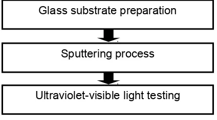
This research was done following the depiction of Picture 1.
Picture 1. Research scheme
Glass substrate preparation process was done using Matsuzawa digital Micro Hardness Tester. UV-vis testing was done using UV-1800 UV-Vis Spectrophotometer by Shimadzu Scientific Instruments Inc. The ultraviolet wavelengths used in this research are between 190 nm to 400 nm and the visible light wavelengths used are between 400 nm to 1100 nm.
3. Results and discussion.
Ultraviolet-visible light testing Glass substrate preparation
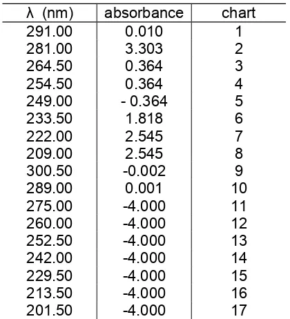
λ (nm) absorbance chart
Table 2. UV-vis testing of glass substrate after silver deposition
λ (nm) absorbance Transmittance
262.50 -4.000
243.00 -4.000
Glass substrate before silver deposition
The glass substrate was observed using Matsuzawa digital Micro Hardness Tester with 40 times magnification before the sputtering process. The result is presented in Picture 2.
Picture 2. The surface of glass substrate before silver deposition
Picture 2 showed that the surface of glass substrate was smooth. It is shown by the contour-less line that observed on the surface of the glass substrate. The less the contour line observed on the surface of the glass substrate is the better the glass substrate preparation. The relation between the wavelengths and the absorbance value is shown by Picture 3.
minimum wavelength absorbed by the glass substrate is equal to 201.50 nm and has absorbance value of -4.000.
Glass substrate after silver deposition
The glass substrate was observed using Matsuzawa digital Micro Hardness Tester with 40 times magnification after the sputtering process. The result is presented in Picture 4.
Picture 4. The surface of glass substrate after silver deposition, was captured using OptilLab
The relation between the wavelengths and the absorbance value is shown by Picture 5.
Picture 5. UV-vis testing result of glass substrate after silver deposition
minimum wavelength absorbed by the glass substrate is equal to 243.00 nm and has absorbance value of -4.000. The difference of the absorbance value was caused by the roughness of the silver thin layer formed on the surface of the glass substrate.
Silver thin layer thickness
The calculation using equation (3), (4), (5) and (6) shown that the reflective value of N1 is equal to 20325.5436 and the reflective value of the silver thin layer n1 for wavelength/ λ1 (243.00 nm) is equal to 201.624892. It is also shown that the reflective value of N2 is equal to 30201.6398 and the reflective value of the silver thin layer n2 for wavelength / λ2 (262.50 nm) is equal to 245.773859. The calculation using equation (7) shown that the silver thin layer thickness d is equal to 4.692663316 nm.
4. Conclusions
The research showed that the absorbance value on the glass substrate was higher after the silver deposition. The research also showed that the smaller the avelength emitted to the glass substrate, the greater the absorbance value changed. We obtained the thickness value of the silver thin layer on the glass substrate was equal to 4.692663316 nm.
Acknowledgment
We would like to acknowledge Arganindya Adiswara for the helpful discussions and comment regarding this article. This research was supported by Faculty of Mathematics and Natural Science, University of Lampung, Indonesia.
References
Blue Photodegradation. Reaktor. Vol. 15, No. 3, 175-181.
[3] Wasa, K., Kitabatake, M & Adachi, H. 2004.Thin Film Materials Technologi Sputtering of Compound Materials.Springer. Germany.
[4] Widodo, Slamet. 2012. Teknologi Pendeposisn Film Tipis Metal Dengan Metode DC-Sputtering. Seminar Nasional Fisika 2012. 76-81. LIPI. Bandung. [5] Struat, R,V. 1983. Vakum Technology, Thin Film and Sputtering. Academic
Press Inc. New York.
[6] Agung, G.F., Hanafie, R.M., dan Mardina, P. 2013. Ekstraksi Silika dari Abu Sekam Padi dengan Pelarut KOH. Konversi. Vol. 2, No. 1, 28-31.
[7] Timuda, Gerald Ensang. 2010. Pengaruh Ketebalan terhadap Sifat Optik
Lapisan Semikonduktor Cu2O yang Dideposisikan dengan Metode Chemical
Bath Deposition (CBD).Jurnal Ilmu Pengetahuann dan teknologi TELAAH Vol. 28, 1-5, November 2010.LIPI.Tangerang.