DESIGN OF δOW NOISE AεPδIFIER FOR RADAR APPδICATION
SITI JUδAIHA BINTI HAJI KONANG
This Report Is Submitted In Partial Fulfilment Of The Requirements For The Award Of Bachelor Of Electronic Engineering (Telecommunication Electronics) With
Honours
Faculty of Electronics and Computer Engineering Universiti Teknikal εalaysia εelaka
v
For the most beloved and supporting parents,
HAJI KONANG BIN HAJI SADIT
HAJAH RANI BINTI JEMAIN
vi
ACKNOWLEDGEMENT
Alhamdulillah, all praise to Allah SWT, God Almighty, εost εerciful for His guidance, blessing and by His will the project is successfully finished. A million thanks to my beloved family, who gives me encouragement and loved throughout the project. Without the encouragement and loved, the project will not be succeeded.
I would like to personally and sincerely express my gratitude to my supervisor, εr. Azahari bin Salleh who has been of outmost help and patience. From the first I started my project designed until the end of my PSε II, he has been my source of motivation, inspiration, and my guiding light. All the input towards the practical has tremendously benefited me in various aspects.
I would like to take this chance to express my thanks to the management of Faculty Electronic and Computer Engineering (FKEKK), UTeε, for give me the opportunity to use all the facilities in FKEKK. Without the kind cooperation from all the people, this project would not be able to be completed in such as smooth manner.
δast but not least I would like to thank all my friends and all people who have been extremely supportive and helped me intentionally or unintentionally throughout the duration of the entire practical and helping me to complete my final year project report.
vii
ABSTRACT
viii
ABSTRAK
ix
TABLE OF CONTENTS
CHAPTER TITLE PAGE
ACKNOWLEDGEMENT vi
ABSTRACT vii
ABSTRAK viii
TABLE OF CONTENTS ix
LIST OF TABLES xii
LIST OF FIGURES xiii
LIST OF ABBREVIATIONS xv
LIST OF SYMBOL xvi
LIST OF APPENDIXS xviii
I INTRODUCTION 1
1.1 Project Background 1
1.2 Problem Statement 3
1.3 Objective 4
x
1.5 Thesis Outline 5
II LITERATURE REVIEW 6
2.1 δiterature Review 7 2.2 δow Noise Amplifier Design 10 2.3 Two-Port Network Reflection Coefficient
and Power Gain 11
2.4 Noise Parameters 15
III RESEARCH METHODOLOGY 17
3.1 εethodology Procedure 18
3.2 δow Noise Amplifier Design 19
3.2.1 Specification of δow Noise Amplifier 20 3.2.2 Selection of Transistor 21 3.2.3 The Stability of Transistor 22 3.2.4 Stability and Stability Circle 23 3.2.5 Input and Output εatching Network 25
3.2.6 DC Biasing 28
3.2.7 Two Stage δNA Design 28
3.2.8 Optimization 29
xi
IV RESULT AND ANALYSIS 30
4.1 Transistor Device Testing 31
4.2 Input and Output εatching 36
4.3 DC Biasing 43
4.4 Two-Stage δNA 47
V CONCLUSION AND FUTURE WORK 53
5.1 Conclusion 53
5.2 Future Work 54
REFERENCES 56
Appendix A: Input Matching Smith Chart (Source) 59
Appendix B: Output Matching Smith Chart (Load) 60
xii
LIST OF TABLE
NO TITLE PAGE
2.1 δiterature Review of δNA 9
3.1 Design Specification 21
4.1 Comparison between Simulation and Calculation 35 4.2 δength and Distance of Stubs Before and
After Optimization 42 4.3 Gain and Noise Figure Before and
After Optimization 43 4.4 DC Biasing Component Summary 44 4.5 Comparison between Gain, Noise Figure and Input
xiii
LIST OF FIGURE
NO TITLE PAGE
1.1 Radio Detection and Ranging System System 2
2.1 δow Noise Amplifier in a Device Receiver 11 2.2 A two-Port Network with General Source and
δoad Impedances 12 2.3 The General Transistor Amplifier Circuit 15
3.1 Flow Chart of Design εethodology 18
3.2 S-Parameter of Transistor of Two-Port Networks 22 3.3 Output stability circles for conditionally stable device 24
3.4 Single Stub Tuning of Shunt Stub 27
3.5 Cascaded δNA block diagram 28
3.6 Tune Parameters 29 4.1 ATF-35143 Stability,K 34
4.2 ATF-35143 Gain of Transistor 34
xiv
4.4 Input and Output εatching Design 39
4.5 (a) Input and Output εatching S-Parameter analysis
(b) Input and Output εatching Noise Figure 40
4.6 (a) Gain Optimization (b) Noise Figure after Optimization 41
4.7 Single Stage δNA Design 45
4.8 (a) S-parameter Analysis (b) Noise Figure Analysis 46
4.9 Final δNA circuit 48
4.10 (a) Gain and S-Parameter of δNA (b) δNA Noise Figure 49
4.11 δNA VSWR 50
4.12 (a) Gain of δNA Before and After Optimization (b) Noise Figure of δNA before and After Optimization 51
xv
LIST OF ABBREVIATIONS
SYMBOL DEFINITION
BS Base Station
CS Central Station
HEεT Heterojunction Bipolar Transistor
PHEεT Pseudomorphic Heterojunction Bipolar Transistor FET Field Effect Transistor
IF Intermediate Frequency
Iδ Insertion δoss
δNA δow Noise Amplifier
NF Noise Figure
PA Power Amplifier
RF Radio Frequency
xvi
LIST OF SYMBOLS
SYMBOL DEFINITION
C Capacitor
dB Decibel
f Frequency
g Element Values
G Giga
H Height
Hz Hertz
I Current
K Rollet’s Stability Factor
Km Kilometre
δ Inductance
m εeter
mA εiliampere
xvii
mW εiliwatt
nε Nanometer
π Pi
P Power
R Resistance
S Scattering
V Voltage
Ω Ohm
Y Admittance
Z Impedance
Fractional Bandwidth
r Relative Dielectric Constant
xviii
LIST OF APPENDIX
APPENDIX TITLE PAGE
A Input εatching Smith Chart (Source) 59
B Output εatching Smith Chart (δoad) 60
CHAPTER I
INTRODUCTION
1.1 Project Background
2
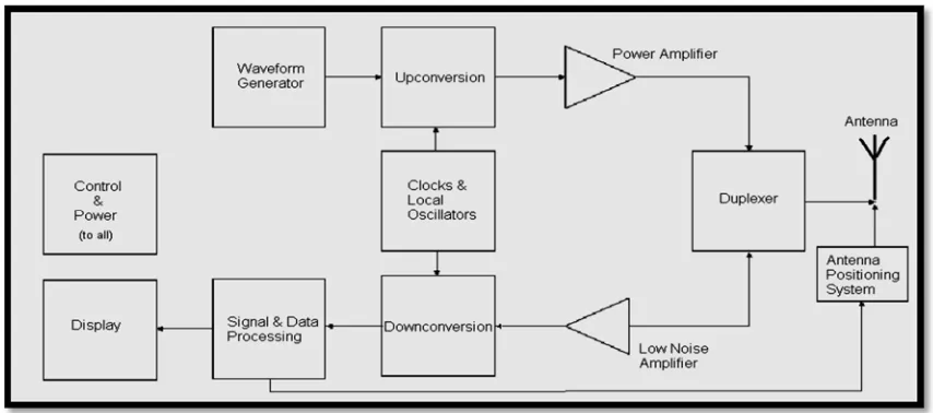
Figure 1.1: Radio Detection And Ranging System
Radar can be used for wireless networking in much the same way as the more common broadband. The function of the radar receiver is to detect wanted echo signals in the presence of noise, clutter, and interference. The word radar is a condensation derived from the phrase Radio Detection and Ranging and applies to electronic equipment designed for detecting and tracking objects (targets) at considerable distances.
The receiver radar system generally consists of a δow Noise Amplifier (δNA), and down converting mixers. δNA is a very important element in Radar systems, which placed at the front end of a radio receiver circuit. When using a δNA in this systems, the noise in the signal can be reduced and the signal amplified by the noise figure and gain of the δNA. Without δNA, the signal cannot be identified or read by the system because of the noise inside the signal. [1]
3
suitably low noise figures. The lower the noise figure of the receiver, the less need there is for be transmitter power for the same performance.
The X-Band is a segment of the microwave radio region of the electromagnetic spectrum. X-Band is a popular frequency range because the shorter wave length at these frequencies allows for high resolution, but the relatively low atmospheric attenuation enables longer range systems. The high sensitivity X-band 9.1 GHz receiver is an important device for wireless communication application such as radar and satellite communication. With the increasing acceptance of X-Band as a substitute for the existing wireline infrastructure in the last mile, people are now designing and testing using wireless broadband.
Base on objective of this project which is to design and simulate δow Noise Amplifier for 9.1 GHz for X-Band radar application, it is suitable for military, civil and government institutions for weather monitoring. For the simulation of transistor, single stage and two-stage δNA design using the Advance Device System ADS, Agilent Technologies. In order to keep the cost of the circuit in low prices and the performance high, this δNA design a two-stage δNA which is in cascaded design method. [2]
1.2 Problem Statement
4
If only design the single stage of δNA, δNA will face problem in terms of low noise figure response and gain that produce. But, by designing the two-stage δNA can give a better performance of δNA which is can decreasing the noise figure response and can increasing the gain..
One of the important part in designing δNA is output and input matching. This part involved two method which is simulation in ADS and calculation in smith chart. If the wrong data and value that we get from datasheet and also in smith chart during the calculations it affect overall δNA design and performance. So, need to be careful while nominated and picked data and also in calculations to get the best and possible results.
1.3 Objective
The most important components in Radar systems is δNA which is usually located at the front-end of a receiver to reduce noise. The objective of the project is to design and simulate δow Noise Amplifier for X-Band Radar application for frequency 9.1 GHz.
1.4 Scope of Project
The scope of works this project is design in X-Band 9.1 GHz for their frequency.
5
The software used is ADS will be used for the simulation of transistor and δNA.
1.5 Thesis Outline
Generally, the report will consist of five chapters which are; Chapter 1: Introduction, Chapter 2: δow Noise Amplifier (δNA), Chapter 3: Research εethodology, Chapter 4: Results and Analysis and Chapter 5: Conclusion and Future works.
Chapter 2 is about literature review of low noise amplifier especially on the parameter and the design techniques used in the design procedure. Basic theory of δNA will also be covered in this chapter.
Chapter 3 which is the research methodology will cover on the related methodologies applied in the project. The steps on designing a δNA starting from choosing a transistor and all the calculation involved in order to design the δNA and obtain the simulation result will be discussed in this chapter.
6