A dielectric superstrate layer above a microstrip patch antenna has remarkable effects on its gain and resonant characteristics. This paper experimentally investigates the effect of a superstrate layer for high gain on microstrip patch antennas. We measured the gain of antennas with and without a superstrate and found that the gain of a single patch with a superstrate was enhanced by about 4 dBi over the one without a superstrate at 12 GHz. The impedance bandwidths of a single patch with and without a superstrate for VSWR < 2 were above 11%. The designed 2×8 array antenna using a superstrate had a high gain of over 22.5 dB and a wide impedance bandwidth of over 17%.
Keywords: High-gain, broadband, superstrate layer, microstrip antenna, stacked patch.
Manuscript received Nov. 26, 2002; revised Mar. 27, 2003.
Wonkyu Choi (phone:+ 82 42 860 4999, email: [email protected]), Cheol-Sik Pyo (email: [email protected]), and Jae-Ick Choi (email: [email protected]) are with Radio & Broadcasting Research Laboratory, ETRI, Daejeon, Korea.
Yong Heui Cho (email: [email protected]) is with Division of Information Communication and Radio Engineering, Mokwon University, Daejeon, Korea.
I. Introduction
Recently, microstrip antennas having attractive features, such as low profile, light weight, and easy fabrication, are being widely used. Microstrip antennas also possess major shortcomings, such as narrow impedance bandwidth and low efficiency and gain, which seriously limit their application. Many broadband techniques for microstrip antennas have been reported [1], [2], and to overcome the disadvantage of low gain, some papers have proposed gain enhancement methods using multiple superstrates [3], [4]. However, the presence of superstrates above an antenna may adversely affect the antenna’s basic performance characteristics, such as gain, radiation resistance, and efficiency. For this reason, it is important to analyze superstrate effects, so adequate superstrate parameters can be chosen to enhance gain and radiation efficiency. It has been reported that high gain can be achieved if the substrate and superstrate layers are used appropriately [3]. This paper compares the gain of a single patch with a superstrate with that of a single patch without a superstrate and reports the experimental results for a 2×8 array antenna with a superstrate and a 4×8 array antenna without a superstrate. We also present the details of the proposed antenna design.
II. Design of the Antenna Element and
Simulation Results
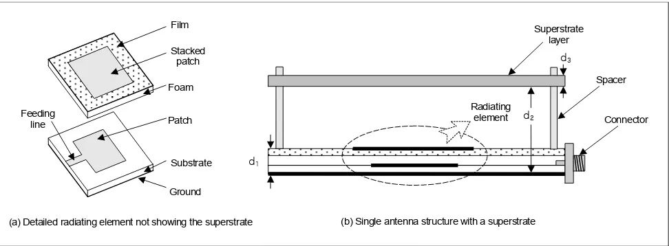
Figure 1 depicts the proposed configuration designed to achieve a high gain single element antenna. Except for the superstrate, the radiating element itself is composed of the layer structure described in [5]. As Fig. 1(a) shows, the lower patch and feeding line are on the substrate with εr= 2.17
A High-Gain Microstrip Patch Array
Antenna Using a Superstrate Layer
Fig. 1. Detailed radiating element not showing the superstrate and a single antenna structure with a superstrate.
(a) Detailed radiating element not showing the superstrate (b) Single antenna structure with a superstrate
and thickness = 0.508 mm, and the stacked patch on the thin film is supported by foam (εr= 1.06, 2 mm). Being very thin (0.04 mm) with respect to the wavelength, the film hardly affects radiation efficiency. Figure 1(b) shows the whole antenna structure for high gain. It is composed of the radiating element and the superstrate with εr= 6.4 and thickness d3 =
1.27 mm (0.13 λg at 12 GHz). The superstrate is placed above
the radiating patch at a distance d2 = 12.75 mm (0.51 λ0 at
12 GHz), where λ0 is the wavelength in free space and λg is the
wavelength in the medium of the superstrate (εr= 6.4). Once
d1 and d3 are specified, d2 can be chosen through trial and error
for high gain. With a configuration like that in Fig. 1(b), it is convenient to adjust the distance d2. By simply adjusting the
distance d2, the resonance condition for high gain can be
obtained.
The resonance condition for high gain can be satisfied as d1
is electrically a quarter wavelength and d2 is half a wavelength
[3], [4], [6]. However, for a microstrip patch antenna, d1 with a λg/4 thickness is too thick. In this case, problems such as high
surface wave and cross-polarization can occur. To overcome these problems, [7] reported that the optimal gain can be obtained by adjusting the distance d2 for various thicknesses of
d1. Therefore, for different thicknesses of d1 and d3, there is a
different resonance thickness d2.
Based on the geometry shown in the Fig. 1, the simulation results using the commercial tool ENSEMBLE are shown in Fig. 2. In Fig. 2, the gain of a single patch with a superstrate is compared with that of a single patch without a superstrate. With a superstrate, the gain was about 13.9 dBi and without a superstrate, it was about 9.3 dBi. Thus, a gain enhancement of about 4 dBi was obtained over the gain of the patch without a superstrate at 12 GHz. The impedance bandwidths of single patches with and without a superstrate for VSWR < 2 were above 11%.
11.0 11.5 12.0 12.5 13.0
-30
Gain without superstrate Gain with superstrate Return loss without superstrate Return loss with superstrate
Fig. 2. Simulated results of the single patch with and without the superstrate.
Fig. 3. The 2×8 array structure not showing the superstrate.
Stacked patch
Lower
patch λ/4 transformer
Feeding
III. Design of Array Antenna
Figure 3 shows the designed array structure. The array was designed using a single radiating element (Fig. 1(b)) and corporate feeding method. The element spacing of this array antenna was 1.16 λ0 at 12 GHz to minimize coupling.
Fig. 4. Photograph of the fabricated 2×8 array antenna with a superstrate.
(a) Assembled antenna structure
(b) Disassembled antenna structure
10 11 12 13 14 Return Loss(Sim .) Return Loss(Meas.)
(a) The 4×8 array antenna without a superstrate
(b) The 2×8 array antenna with a superstrate
Fig. 5. Simulated and measured results of an antenna with and without a superstrate.
wavelength in free space, the grating lobes were reduced by the superstrate.
IV. Fabrication and Measurement
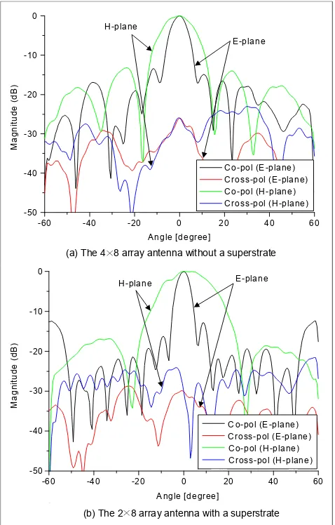
For this investigation, we fabricated a 2×8 array antenna with a superstrate and a 4×8 array antenna without a superstrate. Figure 4 shows a photograph of the fabricated 2×8 array antenna with a superstrate. We compared the measured results with the simulation results (Fig. 5) and measured the radiation patterns at 12 GHz (Fig. 6).
-60 0 20
(a) The 4×8 array antenna without a superstrate
(b) The 2×8 array antenna with a superstrate
Fig. 6. Measured radiation patterns of an antenna with and without a superstrate at 12 GHz.
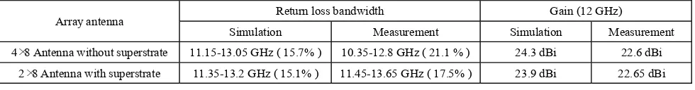
Table 1. Comparison for impedance bandwidth and gain.
Return loss bandwidth Gain (12 GHz) Array antenna
Simulation Measurement Simulation Measurement
4×8 Antenna without superstrate 11.15-13.05 GHz ( 15.7% ) 10.35-12.8 GHz ( 21.1 % ) 24.3 dBi 22.6 dBi
2×8 Antenna with superstrate 11.35-13.2 GHz ( 15.1% ) 11.45-13.65 GHz ( 17.5% ) 23.9 dBi 22.65 dBi
Table 2. Comparison for radiation pattern.
Half-power beamwidth Array antenna Sidelobe level Cross-pol level
E-plane H-plane
4×8 Antenna without superstrate Below -12dB Below -25dB About 7° About 13.5°
2×8 Antenna with superstrate Below -12dB Below -30dB About 5.5° About 20.8°
cross-polarization level was lower than -30 dB for the broadside direction. The half power beamwidths were about 5.5° in the E-plane and 20.8° in the H-plane. The gains of both antennas were about 22.6 dBi in the former and 22.65 dBi in the latter at 12 GHz.
The experimental impedance bandwidths for VSWR<2 were both above 17%. A summary of the designed antennas is given in Tables 1 and 2. The tables reveal that the designed 2×8 array antenna with the superstrate had almost the same results as those of the 4×8 array antenna without the superstrate.
V. Conclusion
This paper introduced experimentally the effect of a superstrate layer for high gain on a microstrip patch antenna. The radiating element with broadband and high radiation efficiency was designed to enhance the narrow bandwidth characteristic by a superstrate with high permittivity. We compared the gain of a single patch with a superstrate to that of a single patch without a superstrate and gave the experimental results of a 2×8 array antenna with a superstrate and a 4×8 array antenna without a superstrate. The designed 2×8 array antenna using a superstrate had a high gain of over 22.5 dBi and a wide impedance bandwidth of over 17%. The proposed antenna will be useful for high gain systems requiring a broadband.
References
[1] A. Sabban, “A New Broadband Stacked Two-layer Microstrip Antenna,” IEEE AP-S Int. Symp. Digest, vol. 21, May 1983, pp. 63-66.
[2] Jang Y. W., “Wide-Band T-Shaped Microstrip-Fed Twin-Slot Array Antenna,” ETRI J., vol.23, no.1, Mar. 2001, pp.33-38. [3] D. R. Jackson and N. G. Alexopoulos, “Gain Enhancement
Methods for Printed Circuit Antennas,” IEEE Trans. Antennas Propagat., vol. 33, no. 9, Sept. 1985, pp.976-987.
[4] H. Y. Yang and N. G. Alexopoulos, “Gain Enhancement Methods for Printed Circuit Antennas through Multiple Superstrates,” IEEE Trans. Antennas Propagat., vol. 35, no. 7, July 1987, pp.860-863. [5] Wonkyu Choi, Cheolsig Pyo, and Jaeick Choi, “Broadband
Circularly Polarized Corner-truncated Square Patch Array Antenna,” IEEE AP-S Int. Symp., vol. 2, June 2002, pp.220-223. [6] Xiao Hai Shen, P. Delmotte, and Guy A. E. Vandenbosch, “Effect
of Superstrate on Radiated Field of Probe Fed Microstrip Patch Antenna,” IEE Proc. Microw. Antennas Propagat., vol. 148, no. 3, June 2001, pp. 141-146.
Wonkyu Choi received the BS and MS degrees in radio engineering from Kyunghee University, Kyonggi, Korea, in 1999 and 2001. In 2001, he joined the Electronics and Telecommunications Research Institute, Daejeon, Korea, as a member of the Research Staff in the Radio & Broadcasting Research Laboratory. His research interests include microwave and millimeter wave antenna and RF passive components.
Yong Heui Cho received the BS degree in electronic engineering from Kyungpook National University, Daegu, Korea, in 1998, the MS and PhD degrees in electrical engineering from Korea Advanced Institute of Science and Technology (KAIST), Daejeon, Korea, in 2000 and 2002. From 2002 to 2003, he was a Senior Research Staff with Electronics and Telecommunications Research Institute (ETRI). In 2003, he joined the Division of Information Communication and Radio Engineering, Mokwon University, Daejeon, Korea, where he is currently a full-time Lecturer. His research interests include the dispersion and coupling characteristics in waveguides and transmission lines.
Cheol-Sik Pyo received the BS degree in electronic engineering from Yonsei University in 1991, the MS degree in electrical engineering from Korea Advanced Institute of Science and Technology (KAIST) in 1999. Since 1991, he has been a Senior Engineer at Electronics and Telecommunications Research Institute (ETRI). His research interests include antenna and radio systems.