XR-2206
...the analog plus company
TM
Monolithic
Function Generator
Rev. 1.03
June 1997-3
FEATURES
D
Low-Sine Wave Distortion, 0.5%, Typical
D
Excellent Temperature Stability, 20ppm/
°
C, Typ.
D
Wide Sweep Range, 2000:1, Typical
D
Low-Supply Sensitivity, 0.01%V, Typ.
D
Linear Amplitude Modulation
D
TTL Compatible FSK Controls
D
Wide Supply Range, 10V to 26V
D
Adjustable Duty Cycle, 1% TO 99%
APPLICATIONS
D
Waveform Generation
D
Sweep Generation
D
AM/FM Generation
D
V/F Conversion
D
FSK Generation
D
Phase-Locked Loops (VCO)
GENERAL DESCRIPTION
The XR-2206 is a monolithic function generator
integrated circuit capable of producing high quality sine,
square, triangle, ramp, and pulse waveforms of
high-stability and accuracy. The output waveforms can be
both amplitude and frequency modulated by an external
voltage. Frequency of operation can be selected
externally over a range of 0.01Hz to more than 1MHz.
The circuit is ideally suited for communications,
instrumentation, and function generator applications
requiring sinusoidal tone, AM, FM, or FSK generation. It
has a typical drift specification of 20ppm/
°
C. The oscillator
frequency can be linearly swept over a 2000:1 frequency
range with an external control voltage, while maintaining
low distortion.
ORDERING INFORMATION
Part No.
Package
Operating
Temperature Range
XR-2206M
16 Lead 300 Mil CDIP
-55
°
C to +125
°
C
XR-2206P
16 Lead 300 Mil PDIP
–40
°
C to +85
°
C
XR-2206CP
16 Lead 300 Mil PDIP
0
°
C to +70
°
C
XR-2206D
16 Lead 300 Mil JEDEC SOIC
0
°
C to +70
°
C
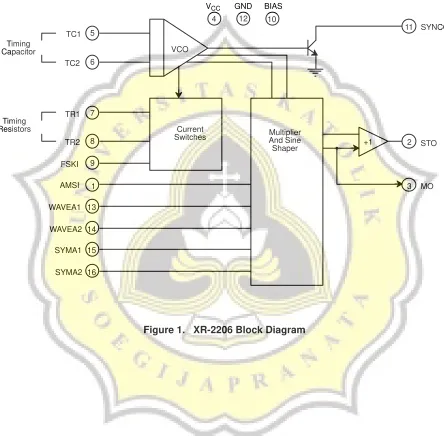
XR-2206
11 SYNCO
VCO
4
V
CC
12
GND
10
BIAS
Timing
Capacitor
5
TC1
6
TC2
Timing
Resistors
7
TR1
8
TR2
9
FSKI
1
AMSI
Current
Switches
Multiplier
And Sine
Shaper
2
STO
3
MO
13
WAVEA1
14
WAVEA2
15
SYMA1
16
SYMA2
Figure 1. XR-2206 Block Diagram
+1
XR-2206
16 Lead PDIP, CDIP (0.300”)
SYMA2
SYMA1
WAVEA2
WAVEA1
GND
SYNCO
BIAS
FSKI
AMSI
STO
MO
V
CC
TC1
TC2
TR1
TR2
1
2
3
4
5
6
7
8
16
15
14
13
12
11
10
9
AMSI
STO
MO
V
CC
TC1
TC2
TR1
TR2
SYMA2
SYMA1
WAVEA2
WAVEA1
GND
SYNCO
BIAS
FSKI
16 Lead SOIC (Jedec, 0.300”)
16
1
9
8
2
3
4
5
6
7
15
14
13
12
11
10
PIN DESCRIPTION
Pin #
Symbol
Type
Description
1
AMSI
I
Amplitude Modulating Signal Input.
2
STO
O
Sine or Triangle Wave Output.
3
MO
O
Multiplier Output.
4
V
CC
Positive Power Supply.
5
TC1
I
Timing Capacitor Input.
6
TC2
I
Timing Capacitor Input.
7
TR1
O
Timing Resistor 1 Output.
8
TR2
O
Timing Resistor 2 Output.
9
FSKI
I
Frequency Shift Keying Input.
10
BIAS
O
Internal Voltage Reference.
11
SYNCO
O
Sync Output.
This output is a open collector and needs a pull up resistor to V
CC
.
12
GND
Ground pin.
13
WAVEA1
I
Wave Form Adjust Input 1.
14
WAVEA2
I
Wave Form Adjust Input 2.
15
SYMA1
I
Wave Symetry Adjust 1.
16
SYMA2
I
Wave Symetry Adjust 2.
XR-2206
DC ELECTRICAL CHARACTERISTICS
Test Conditions: Test Circuit of Figure 2
Vcc
= 12V, T
A
= 25
°
C, C = 0.01
m
F, R
1
= 100k
W
, R
2
= 10k
W
, R
3
= 25k
W
Unless Otherwise Specified. S
1
open for triangle, closed for sine wave.
XR-2206M/P
XR-2206CP/D
Parameters
Min.
Typ.
Max.
Min.
Typ.
Max.
Units
Conditions
General Characteristics
Single Supply Voltage
10
26
10
26
V
Split-Supply Voltage
+5
+13
+5
+13
V
Supply Current
12
17
14
20
mA
R
1
10kW
Oscillator Section
Max. Operating Frequency
0.5
1
0.5
1
MHz
C = 1000pF, R
1
= 1kW
Lowest Practical Frequency
0.01
0.01
Hz
C = 50mF, R
1
= 2MW
Frequency Accuracy
+1
+4
+2
% of f
o
f
o
= 1/R
1
C
Temperature Stability
Frequency
+10
+50
+20
ppm/
°
C
0
°
C
T
A
70
°
C
R
1
= R
2
= 20kW
Sine Wave Amplitude Stability
2
4800
4800
ppm/
°
C
Supply Sensitivity
0.01
0.1
0.01
%/V
V
LOW
= 10V, V
HIGH
= 20V,
R
1
= R
2
= 20kW
Sweep Range
1000:1
2000:1
2000:1
f
H
= f
L
f
H
@ R
1
= 1kW
f
L
@ R
1
= 2MW
Sweep Linearity
10:1 Sweep
2
2
%
f
L
= 1kHz, f
H
= 10kHz
1000:1 Sweep
8
8
%
f
L
= 100Hz, f
H
= 100kHz
FM Distortion
0.1
0.1
%
+10% Deviation
Recommended Timing Components
Timing Capacitor: C
0.001
100
0.001
100
mF
Figure 5
Timing Resistors: R
1
& R
2
1
2000
1
2000
kW
Triangle Sine Wave Output
1
Figure 3
Triangle Amplitude
160
160
mV/kW
Figure 2, S
1
Open
Sine Wave Amplitude
40
60
80
60
mV/kW
Figure 2, S
1
Closed
Max. Output Swing
6
6
Vp-p
Output Impedance
600
600
W
Triangle Linearity
1
1
%
Amplitude Stability
0.5
0.5
dB
For 1000:1 Sweep
Sine Wave Distortion
Without Adjustment
2.5
2.5
%
R
1
= 30kW
With Adjustment
0.4
1.0
0.5
1.5
%
See Figure 7 and Figure 8
Notes
1
Output amplitude is directly proportional to the resistance, R
3
, on Pin 3. See Figure 3.
2
For maximum amplitude stability, R
3
should be a positive temperature coefficient resistor.
Bold face parameters
are covered by production test and guaranteed over operating temperature range.
XR-2206
DC ELECTRICAL CHARACTERISTICS
(CONT’D)
XR-2206M/P
XR-2206CP/D
Parameters
Min.
Typ.
Max.
Min.
Typ.
Max.
Units
Conditions
Amplitude Modulation
Input Impedance
50
100
50
100
kW
Modulation Range
100
100
%
Carrier Suppression
55
55
dB
Linearity
2
2
%
For 95% modulation
Square-Wave Output
Amplitude
12
12
Vp-p
Measured at Pin 11.
Rise Time
250
250
ns
C
L
= 10pF
Fall Time
50
50
ns
C
L
= 10pF
Saturation Voltage
0.2
0.4
0.2
0.6
V
I
L
= 2mA
Leakage Current
0.1
20
0.1
100
mA
V
CC
= 26V
FSK Keying Level (Pin 9)
0.8
1.4
2.4
0.8
1.4
2.4
V
See section on circuit controls
Reference Bypass Voltage
2.9
3.1
3.3
2.5
3
3.5
V
Measured at Pin 10.
Notes
1
Output amplitude is directly proportional to the resistance, R
3
, on Pin 3. See Figure 3.
2
For maximum amplitude stability, R
3
should be a positive temperature coefficient resistor.
Bold face parameters
are covered by production test and guaranteed over operating temperature range.
Specifications are subject to change without notice
ABSOLUTE MAXIMUM RATINGS
Power Supply
. . .
26V
Power Dissipation
. . .
750mW
Derate Above 25
°
C
. . .
5mW/
°
C
Total Timing Current
. . .
6mA
Storage Temperature
. . .
-65
°
C to +150
°
C
SYSTEM DESCRIPTION
The XR-2206 is comprised of four functional blocks; a
voltage-controlled oscillator (VCO), an analog multiplier
and sine-shaper; a unity gain buffer amplifier; and a set of
current switches.
The VCO produces an output frequency proportional to
an input current, which is set by a resistor from the timing
terminals to ground. With two timing pins, two discrete
output frequencies can be independently produced for
FSK generation applications by using the FSK input
control pin. This input controls the current switches which
select one of the timing resistor currents, and routes it to
the VCO.
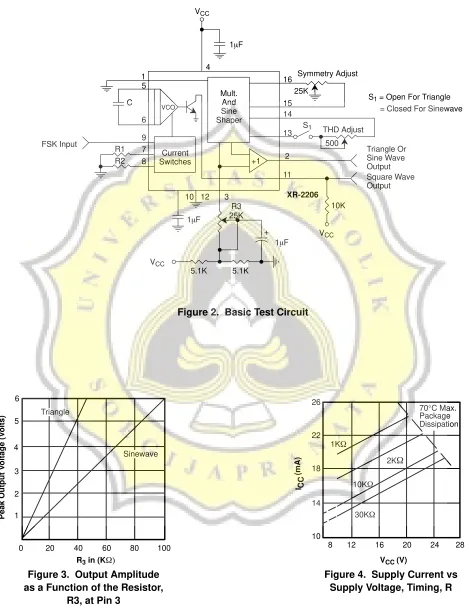
XR-2206
5
Figure 2. Basic Test Circuit
Symmetry Adjust
25K
1
6
7
8
9
11
3
2
13
14
15
16
4
10 12
XR-2206
1
m
F
V
CC
C
R1
R2
FSK Input
S
1
THD Adjust
500
Triangle Or
Sine Wave
Output
Square Wave
Output
V
CC
10K
1
m
F
R3
25K
5.1K
5.1K
V
CC
1
m
F
Current
Switches
Mult.
And
Sine
Shaper
+1
VCO
+
S
1
= Open For Triangle
= Closed For Sinewave
Figure 3. Output Amplitude
as a Function of the Resistor,
R3, at Pin 3
ÎÎÎÎÎÎÎÎÎÎ
ÎÎÎÎÎÎÎÎÎÎ
ÎÎÎÎÎÎÎÎÎÎ
ÎÎÎÎÎÎÎÎÎÎ
ÎÎÎÎÎÎÎÎÎÎ
ÎÎÎÎÎÎÎÎÎÎ
ÎÎÎÎÎÎÎÎÎÎ
ÎÎÎÎÎÎÎÎÎÎ
ÎÎÎÎÎÎÎÎÎÎ
ÎÎÎÎÎÎÎÎÎÎ
Triangle
Sinewave
26
22
18
14
10
8
12
16
20
24
28
70
°
C Max.
Package
Dissipation
1K
W
2K
W
10K
W
30K
W
Figure 4. Supply Current vs
Supply Voltage, Timing, R
0
20
40
60
80
100
1
2
3
4
5
6
Peak Output V
oltage (V
olts)
R
3
in (KW)
I CC
(mA)
V
CC
(V)
XR-2206
ÁÁÁÁÁ
ÁÁÁÁÁ
MINIMUM TIMING R
ÎÎÎÎÎÎÎÎÎÎÎÎ
ÎÎÎÎÎÎÎÎÎÎÎÎ
ÎÎÎÎÎÎÎÎÎÎÎÎ
ÎÎÎÎÎÎÎÎÎÎÎÎ
ÎÎÎÎÎÎÎÎÎÎÎÎ
ÎÎÎÎÎÎÎÎÎÎÎÎ
ÎÎÎÎÎÎÎÎÎÎÎÎ
ÎÎÎÎÎÎÎÎÎÎÎÎ
ÎÎÎÎÎÎÎÎÎÎÎÎ
ÎÎÎÎÎÎÎÎÎÎÎÎ
ÎÎÎÎÎÎÎÎÎÎÎÎ
ÎÎÎÎÎÎÎÎÎÎÎÎ
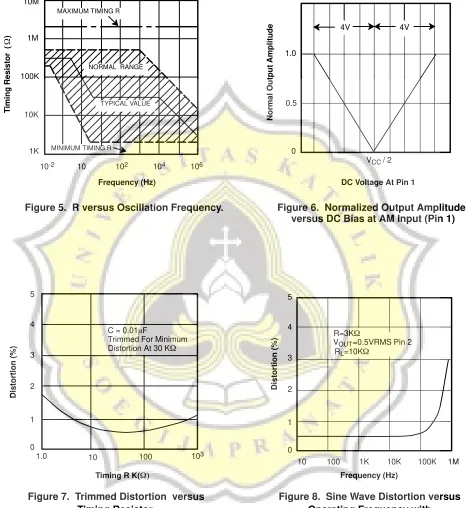
Figure 5. R versus Oscillation Frequency.
ÎÎÎÎÎÎÎÎÎÎÎ
ÎÎÎÎÎÎÎÎÎÎÎ
ÎÎÎÎÎÎÎÎÎÎÎ
ÎÎÎÎÎÎÎÎÎÎÎ
ÎÎÎÎÎÎÎÎÎÎÎ
ÎÎÎÎÎÎÎÎÎÎÎ
ÎÎÎÎÎÎÎÎÎÎÎ
ÎÎÎÎÎÎÎÎÎÎÎ
ÎÎÎÎÎÎÎÎÎÎÎ
ÎÎÎÎÎÎÎÎÎÎÎ
4V
4V
10M
1M
100K
10K
1K
10
-2
10
10
2
ÁÁÁÁÁÁ
ÁÁÁÁÁÁ
MAXIMUM TIMING R
V
CC
/ 2
DC Voltage At Pin 1
Frequency (Hz)
T
iming Resistor
W
0
0.5
1.0
Normal Output
Amplitude
Figure 6. Normalized Output Amplitude
versus DC Bias at AM Input (Pin 1)
Figure 7. Trimmed Distortion versus
Timing Resistor.
Distortion (%)
Timing R K(W)
0
1
2
3
4
5
1.0
10
100
10
3
ÁÁÁÁÁÁÁ
ÁÁÁÁÁÁÁ
ÁÁÁÁÁÁÁ
C = 0.01
m
F
Trimmed For Minimum
Distortion At 30 K
W
Figure 8. Sine Wave Distortion versus
Operating Frequency with
Timing Capacitors Varied.
10
100
1K
10K
100K
1M
0
1
2
3
4
5
Distortion (%)
Frequency (Hz)
ÁÁÁ
R=3K
W
ÁÁÁÁ
ÁÁÁÁ
R
L
=10K
W
ÁÁÁÁÁ
ÁÁÁÁÁ
NORMAL RANGE
ÁÁÁÁÁ
ÁÁÁÁÁ
TYPICAL VALUE
=0.5VRMS Pin 2
V
OUT
()
10
4
10
6
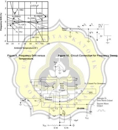
XR-2206
Figure 9. Frequency Drift versus
Temperature.
3
2
1
0
-1
-2
-3
-50
-25
0
25
50
75
125
C=0.01
m
F
R=1M
W
R=2K
W
R=10K
W
R=200K
W
R=1M
W
R=1K
W
R=10K
W
R=2K
W
R=1K
W
Ambient Temperature (C
°
)
Figure 10. Circuit Connection for Frequency Sweep.
Sweep
Input
+
-
V
C
R
I
B
I
C
Rc
I
T
Pin 7
or 8
12
ÁÁ
100
Figure 11. Circuit tor Sine Wave Generation without External Adjustment.
(See Figure 3 for Choice of R
3
)
R=200K
W
Frequency Drift (%)
+
1
5
6
7
8
9
11
3
2
13
14
15
16
4
1 0
1 2
XR-2206
1
m
F
C
R
1
2M
1K
S
1
Triangle Or
Sine Wave Output
Square Wave
Output
200
10K
R
3
50K
5.1K
5.1K
V
CC
10
m
F
1
m
F
R
V
CC
V
CC
Current
Switches
Mult.
And
Sine
Shaper
+1
+
+
VCO
S
1
Closed For Sinewave
3V
XR-2206
0
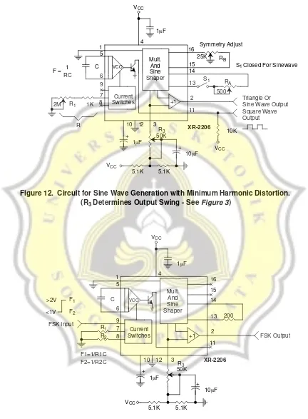
Figure 12. Circuit for Sine Wave Generation with Minimum Harmonic Distortion.
(R
3
Determines Output Swing - See Figure 3)
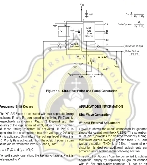
Figure 13. Sinusoidal FSK Generator
Symmetry Adjust
25K
R
B
1
5
6
7
8
9
11
3
2
13
14
15
16
4
1
12
XR-2206
1
m
F
C
1K
R
1
2M
F =
S
1
Triangle Or
Sine Wave Output
Square Wave
Output
R
A
500
10K
5.1K
5.1K
10
m
F
R
3
50K
1
m
F
R
Mult.
And
Sine
Shaper
Current
Switches
V
CC
V
CC
VCO
+
+
+1
V
CC
1
5
6
7
8
9
11
3
2
13
14
15
16
4
10 12
XR-2206
1
m
F
V
CC
C
FSK Input
R
1
R
2
<1V
>2V
F
1
F
2
F1=1/R1C
200
5.1K
5.1K
10
m
F
1
m
F
R
3
50K
F2=1/R2C
V
CC
Mult.
And
Sine
Shaper
VCO
+
+
+1
Current
Switches
S
1
Closed For Sinewave
1
RC
FSK Output
XR-2206
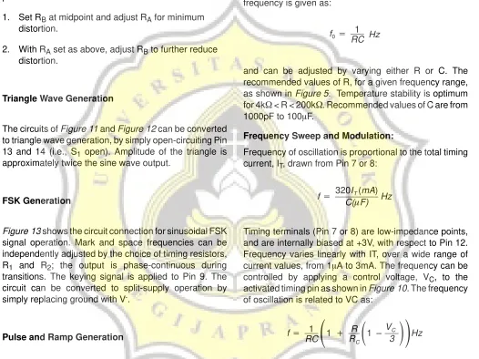
Figure 14. Circuit for Pulse and Ramp Generation.
1
5
6
7
8
9
11
3
2
13
14
15
16
4
10
12
XR-2206
1
m
F
V
CC
C
R
1
R
2
5.1K
5.1K
5.1K
10
m
F
1
m
F
R
3
24K
V
CC
V
CC
Mult.
And
Sine
Shaper
VCO
+1
+
+
Current
Switches
f
+
C
2
ƪ
R
1
1
)
R
2
ƫ
R
1
R
1
)
R
2
Duty Cycle =
Sawtooth Output
Pulse Output
Frequency-Shift Keying
The XR-2206 can be operated with two separate timing
resistors, R
1
and R
2
, connected to the timing Pin 7 and 8,
respectively, as shown in Figure 13. Depending on the
polarity of the logic signal at Pin 9, either one or the other
of these timing resistors is activated. If Pin 9 is
open-circuited or connected to a bias voltage
2V, only
R
1
is activated. Similarly, if the voltage level at Pin 9 is
1V, only R
2
is activated. Thus, the output frequency can
be keyed between two levels. f
1
and f
2
, as:
f
1
= 1/R
1
C and f
2
= 1/R
2
C
For split-supply operation, the keying voltage at Pin 9 is
referenced to V
-
.
Output DC Level Control
The dc level at the output (Pin 2) is approximately the
same as the dc bias at Pin 3. In Figure 11, Figure 12 and
Figure 13, Pin 3 is biased midway between V+ and
ground, to give an output dc level of
V
+
/2.
APPLICATIONS INFORMATION
Sine Wave Generation
Without External Adjustment
Figure 11 shows the circuit connection for generating a
sinusoidal output from the XR-2206. The potentiometer,
R
1
at Pin 7, provides the desired frequency tuning. The
maximum output swing is greater than V
+
/2, and the
typical distortion (THD) is < 2.5%. If lower sine wave
distortion is desired, additional adjustments can be
provided as described in the following section.
The circuit of Figure 11 can be converted to split-supply
operation, simply by replacing all ground connections
with V
-
. For split-supply operation, R
3
can be directly
connected to ground.
XR-2206
With External Adjustment:
The harmonic content of sinusoidal output can be
reduced to -0.5% by additional adjustments as shown in
Figure 12. The potentiometer, R
A
, adjusts the
sine-shaping resistor, and R
B
provides the fine
adjustment for the waveform symmetry. The adjustment
procedure is as follows:
1.
Set R
B
at midpoint and adjust R
A
for minimum
distortion.
2.
With R
A
set as above, adjust R
B
to further reduce
distortion.
Triangle Wave Generation
The circuits of Figure 11 and Figure 12 can be converted
to triangle wave generation, by simply open-circuiting Pin
13 and 14 (i.e., S
1
open). Amplitude of the triangle is
approximately twice the sine wave output.
FSK Generation
Figure 13 shows the circuit connection for sinusoidal FSK
signal operation. Mark and space frequencies can be
independently adjusted by the choice of timing resistors,
R
1
and R
2
; the output is phase-continuous during
transitions. The keying signal is applied to Pin 9. The
circuit can be converted to split-supply operation by
simply replacing ground with V
-
.
Pulse and Ramp Generation
Figure 14 shows the circuit for pulse and ramp waveform
generation. In this mode of operation, the FSK keying
terminal (Pin 9) is shorted to the square-wave output (Pin
11), and the circuit automatically frequency-shift keys
itself between two separate frequencies during the
positive-going and negative-going output waveforms.
The pulse width and duty cycle can be adjusted from 1%
to 99% by the choice of R
1
and R
2
. The values of R
1
and
R
2
should be in the range of 1k
W
to 2M
W
.
PRINCIPLES OF OPERATION
Description of Controls
Frequency of Operation:
The frequency of oscillation, f
o
, is determined by the
external timing capacitor, C, across Pin 5 and 6, and by
the timing resistor, R, connected to either Pin 7 or 8. The
frequency is given as:
f
0
+
1
RC
Hz
and can be adjusted by varying either R or C. The
recommended values of R, for a given frequency range,
as shown in Figure 5. Temperature stability is optimum
for 4k
W
< R < 200k
W
. Recommended values of C are from
1000pF to 100
m
F.
Frequency Sweep and Modulation:
Frequency of oscillation is proportional to the total timing
current, I
T
, drawn from Pin 7 or 8:
f
+
320I
C(
T
(mA)
m
F)
Hz
Timing terminals (Pin 7 or 8) are low-impedance points,
and are internally biased at +3V, with respect to Pin 12.
Frequency varies linearly with IT, over a wide range of
current values, from 1
m
A to 3mA. The frequency can be
controlled by applying a control voltage, V
C
, to the
activated timing pin as shown in Figure 10. The frequency
of oscillation is related to VC as:
f
+
RC
1
ǒ
1
)
R
R
C
ǒ
1
–
V
C
3
Ǔ
Ǔ
Hz
where V
C
is in volts. The voltage-to-frequency conversion
gain, K, is given as:
K
+ ēfńēV
C
+
– 0.32
R
C
C
HzńV
CAUTION:
For safety operation of the circuit, I
T
should be
limited to
3mA.
XR-2206
Output Amplitude:
Maximum output amplitude is inversely proportional to
the external resistor, R
3
, connected to Pin 3 (see
Figure 3). For sine wave output, amplitude is
approximately 60mV peak per k
W
of R
3
; for triangle, the
peak amplitude is approximately 160mV peak per k
W
of
R
3
. Thus, for example, R
3
= 50k
W
would produce
approximately 13V sinusoidal output amplitude.
Amplitude Modulation:
Output amplitude can be modulated by applying a dc bias
and a modulating signal to Pin 1. The internal impedance
at Pin 1 is approximately 100k
W
. Output amplitude varies
linearly with the applied voltage at Pin 1, for values of dc
bias at this pin, within 14 volts of V
CC
/2 as shown in
Figure 6. As this bias level approaches V
CC
/2, the phase
of the output signal is reversed, and the amplitude goes
through zero. This property is suitable for phase-shift
keying and suppressed-carrier AM generation. Total
dynamic range of amplitude modulation is approximately
55dB.
CAUTION:
AM control must be used in conjunction with a
well-regulated supply, since the output amplitude now becomes
a function of V
CC
.
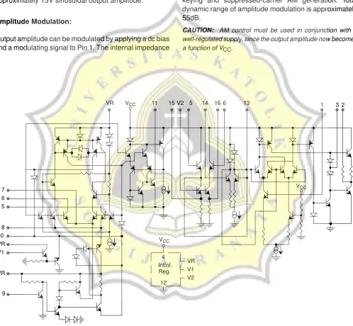
Figure 15. Equivalent Schematic Diagram
2
1
6
16
14
5
13
11
VR
V
CC
15
V2
5
6
7
V
CC
VR
V1
V2
Reg.
Int’nI.
12
4
V
CC
10
VR
V1
VR
8
9
3
XR-2206
A
0.100
0.200
2.54
5.08
A
1
0.015
0.060
0.38
1.52
B
0.014
0.026
0.36
0.66
B
1
0.045
0.065
1.14
1.65
c
0.008
0.018
0.20
0.46
D
0.740
0.840
18.80
21.34
E
1
0.250
0.310
6.35
7.87
E
0.300 BSC
7.62 BSC
e
0.100 BSC
2.54 BSC
L
0.125
0.200
3.18
5.08
α
0
°
15
°
0
°
15
°
D
B
e
B
1
16 LEAD CERAMIC DUAL-IN-LINE
(300 MIL CDIP)
Rev. 1.00
SYMBOL
MIN
MAX
MIN
MAX
INCHES
MILLIMETERS
1
8
9
α
c
E
1
A
L
A
1
Seating
Plane
Base
Plane
16
E
Note: The control dimension is the inch column
XR-2206
16 LEAD PLASTIC DUAL-IN-LINE
(300 MIL PDIP)
Rev. 1.00
16
1
9
8
D
e
B
1
A
1
E
1
E
A
L
B
Seating
Plane
SYMBOL
MIN
MAX
MIN
MAX
INCHES
A
0.145
0.210
3.68
5.33
A
1
0.015
0.070
0.38
1.78
A
2
0.115
0.195
2.92
4.95
B
0.014
0.024
0.36
0.56
B
1
0.030
0.070
0.76
1.78
C
0.008
0.014
0.20
0.38
D
0.745
0.840
18.92
21.34
E
0.300
0.325
7.62
8.26
E
1
0.240
0.280
6.10
7.11
e
0.100 BSC
2.54 BSC
e
A
0.300 BSC
7.62 BSC
e
B
0.310
0.430
7.87
10.92
L
0.115
0.160
2.92
4.06
α
0
°
15
°
0
°
15
°
MILLIMETERS
α
A
2
C
Note: The control dimension is the inch column
e
B
e
A
XR-2206
SYMBOL
MIN
MAX
MIN
MAX
A
0.093
0.104
2.35
2.65
A
1
0.004
0.012
0.10
0.30
B
0.013
0.020
0.33
0.51
C
0.009
0.013
0.23
0.32
D
0.398
0.413
10.10
10.50
E
0.291
0.299
7.40
7.60
e
0.050 BSC
1.27 BSC
H
0.394
0.419
10.00
10.65
L
0.016
0.050
0.40
1.27
α
0
°
8
°
0
°
8
°
INCHES
MILLIMETERS
16 LEAD SMALL OUTLINE
(300 MIL JEDEC SOIC)
Rev. 1.00
e
16
9
8
D
E
H
B
A
L
C
A
1
Seating
Plane
α
Note: The control dimension is the millimeter column
1
XR-2206
NOTICE
EXAR Corporation reserves the right to make changes to the products contained in this publication in order to
im-prove design, performance or reliability. EXAR Corporation assumes no responsibility for the use of any circuits
de-scribed herein, conveys no license under any patent or other right, and makes no representation that the circuits are
free of patent infringement. Charts and schedules contained here in are only for illustration purposes and may vary
depending upon a user’s specific application. While the information in this publication has been carefully checked;
no responsibility, however, is assumed for inaccuracies.
EXAR Corporation does not recommend the use of any of its products in life support applications where the failure or
malfunction of the product can reasonably be expected to cause failure of the life support system or to significantly
affect its safety or effectiveness. Products are not authorized for use in such applications unless EXAR Corporation
receives, in writing, assurances to its satisfaction that: (a) the risk of injury or damage has been minimized; (b) the
user assumes all such risks; (c) potential liability of EXAR Corporation is adequately protected under the
circum-stances.
Copyright 1972 EXAR Corporation
Datasheet June 1997
Reproduction, in part or whole, without the prior written consent of EXAR Corporation is prohibited.
Analog
Multiplexers/Demultiplexers
The MC14051B, MC14052B, and MC14053B analog multiplexers are
digitally–controlled analog switches. The MC14051B effectively implements
an SP8T solid state switch, the MC14052B a DP4T, and the MC14053B a
Triple SPDT. All three devices feature low ON impedance and very low OFF
leakage current. Control of analog signals up to the complete supply voltage
range can be achieved.
•
Triple Diode Protection on Control Inputs
•
Switch Function is Break Before Make
•
Supply Voltage Range = 3.0 Vdc to 18 Vdc
•
Analog Voltage Range (VDD – VEE) = 3.0 to 18 V
Note: VEE must be
v
VSS
•
Linearized Transfer Characteristics
•
Low–noise – 12 nV/
√
Cycle, f
≥
1.0 kHz Typical
•
Pin–for–Pin Replacement for CD4051, CD4052, and CD4053
•
For 4PDT Switch, See MC14551B
•
For Lower RON, Use the HC4051, HC4052, or HC4053 High–Speed
CMOS Devices
ÎÎÎÎÎÎÎÎÎÎÎÎÎÎÎÎÎÎÎÎÎ ÎÎÎÎÎÎÎÎÎÎÎÎÎÎÎÎÎÎÎÎÎ ÎÎÎÎÎÎÎÎÎÎÎÎÎÎÎÎÎÎÎÎÎ ÎÎÎÎÎÎÎÎÎÎÎÎÎÎÎÎÎÎÎÎÎMAXIMUM RATINGS*
ÎÎÎÎ ÎÎÎÎ ÎÎÎÎ ÎÎÎÎSymbol
ÎÎÎÎÎÎÎÎÎÎÎ ÎÎÎÎÎÎÎÎÎÎÎ ÎÎÎÎÎÎÎÎÎÎÎ ÎÎÎÎÎÎÎÎÎÎÎParameter
ÎÎÎÎÎÎ ÎÎÎÎÎÎ ÎÎÎÎÎÎ ÎÎÎÎÎÎValue
ÎÎÎ ÎÎÎ ÎÎÎ ÎÎÎUnit
ÎÎÎÎ ÎÎÎÎ ÎÎÎÎ ÎÎÎÎVDD
ÎÎÎÎÎÎÎÎÎÎÎ ÎÎÎÎÎÎÎÎÎÎÎ ÎÎÎÎÎÎÎÎÎÎÎ ÎÎÎÎÎÎÎÎÎÎÎDC Supply Voltage (Referenced to VEE,
VSS
≥
VEE)
ÎÎÎÎÎÎ
ÎÎÎÎÎÎ
ÎÎÎÎÎÎ
ÎÎÎÎÎÎ
– 0.5 to + 18.0
ÎÎÎ ÎÎÎ ÎÎÎ ÎÎÎ
V
ÎÎÎÎ ÎÎÎÎ ÎÎÎÎ ÎÎÎÎ ÎÎÎÎVin, Vout
ÎÎÎÎÎÎÎÎÎÎÎ ÎÎÎÎÎÎÎÎÎÎÎ ÎÎÎÎÎÎÎÎÎÎÎ ÎÎÎÎÎÎÎÎÎÎÎ ÎÎÎÎÎÎÎÎÎÎÎInput or Output Voltage (DC or Transient)
(Referenced to VSS for Control Inputs and
VEE for Switch I/O)
ÎÎÎÎÎÎ
ÎÎÎÎÎÎ
ÎÎÎÎÎÎ
ÎÎÎÎÎÎ
ÎÎÎÎÎÎ
– 0.5 to VDD + 0.5
ÎÎÎ ÎÎÎ ÎÎÎ ÎÎÎ ÎÎÎ
V
ÎÎÎÎ ÎÎÎÎ ÎÎÎÎ ÎÎÎÎ ÎÎÎÎIin
ÎÎÎÎÎÎÎÎÎÎÎ ÎÎÎÎÎÎÎÎÎÎÎ ÎÎÎÎÎÎÎÎÎÎÎ ÎÎÎÎÎÎÎÎÎÎÎ ÎÎÎÎÎÎÎÎÎÎÎInput Current (DC or Transient),
per Control Pin
ÎÎÎÎÎÎ
ÎÎÎÎÎÎ
ÎÎÎÎÎÎ
ÎÎÎÎÎÎ
ÎÎÎÎÎÎ
±
10
ÎÎÎ ÎÎÎ ÎÎÎ ÎÎÎ ÎÎÎ
mA
ÎÎÎÎ ÎÎÎÎ ÎÎÎÎ ÎÎÎÎIsw
ÎÎÎÎÎÎÎÎÎÎÎ ÎÎÎÎÎÎÎÎÎÎÎ ÎÎÎÎÎÎÎÎÎÎÎ ÎÎÎÎÎÎÎÎÎÎÎSwitch Through Current
ÎÎÎÎÎÎ
ÎÎÎÎÎÎ
ÎÎÎÎÎÎ
ÎÎÎÎÎÎ
±
25
ÎÎÎ ÎÎÎ ÎÎÎ ÎÎÎ
mA
ÎÎÎÎ ÎÎÎÎ ÎÎÎÎ ÎÎÎÎPD
ÎÎÎÎÎÎÎÎÎÎÎ ÎÎÎÎÎÎÎÎÎÎÎ ÎÎÎÎÎÎÎÎÎÎÎ ÎÎÎÎÎÎÎÎÎÎÎPower Dissipation. per Package†
ÎÎÎÎÎÎ ÎÎÎÎÎÎ ÎÎÎÎÎÎ ÎÎÎÎÎÎ
500
ÎÎÎ ÎÎÎ ÎÎÎ ÎÎÎmW
ÎÎÎÎ ÎÎÎÎ ÎÎÎÎTstg
ÎÎÎÎÎÎÎÎÎÎÎ ÎÎÎÎÎÎÎÎÎÎÎ ÎÎÎÎÎÎÎÎÎÎÎStorage Temperature
ÎÎÎÎÎÎ ÎÎÎÎÎÎ ÎÎÎÎÎΖ 65 to + 150
ÎÎÎ ÎÎÎ ÎÎÎ
_
C
ÎÎÎÎ ÎÎÎÎ ÎÎÎÎ ÎÎÎÎTL
ÎÎÎÎÎÎÎÎÎÎÎ ÎÎÎÎÎÎÎÎÎÎÎ ÎÎÎÎÎÎÎÎÎÎÎ ÎÎÎÎÎÎÎÎÎÎÎLead Temperature (8–Second Soldering)
ÎÎÎÎÎÎ ÎÎÎÎÎÎ ÎÎÎÎÎÎ ÎÎÎÎÎÎ
260
ÎÎÎ ÎÎÎ ÎÎÎ ÎÎÎ_
C
* Maximum Ratings are those values beyond which damage to the device may occur.
†Temperature Derating:“P and D/DW” Packages: – 7.0 mW/
_
C From 65
_
C To 125
_
C
Ceramic “L” Packages: – 12 mW/
_
C From 100
_
C To 125
_
C
MC14051B
8–Channel Analog
Multiplexer/Demultiplexer
MC14052B
Dual 4–Channel Analog
Multiplexer/Demultiplexer
MC14053B
Triple 2–Channel Analog
Multiplexer/Demultiplexer
VDD = PIN 16
VSS = PIN 8
VEE = PIN 7
Note: Control Inputs referenced to VSS, Analog Inputs and Outputs reference to VEE. VEE must be
≤
VSS.
INHIBIT
A
B
C
X0
X1
X2
X3
X4
X5
X6
X7
X
4
2
5
1
12
15
14
13
9
10
11
6
CONTROLS
SWITCHES
IN/OUT
COMMON
OUT/IN
3
4
2
5
1
11
15
14
12
9
10
6
CONTROLS
SWITCHES
IN/OUT
13
3
COMMONS
OUT/IN
X
Y
VDD = PIN 16
VSS = PIN 8
VEE = PIN 7
3
5
1
2
13
12
9
10
11
6
CONTROLS
SWITCHES
IN/OUT
14
15
4
X
Y
Z
COMMONS
OUT/IN
VDD = PIN 16
VSS = PIN 8
VEE = PIN 7
INHIBIT
A
B
X0
X1
X2
X3
Y0
Y1
Y2
Y3
INHIBIT
A
B
C
X0
Y0
Y1
Z0
Z1
X1
MOTOROLA
SEMICONDUCTOR TECHNICAL DATA
REV 3
MC14051B
MC14052B
MC14053B
L SUFFIX
CERAMIC
CASE 620
ORDERING INFORMATION
MC14XXXBCP
Plastic
MC14XXXBCL
Ceramic
MC14XXXBD
SOIC
TA = – 55
°
to 125
°
C for all packages.
ÎÎÎÎÎÎÎÎÎÎÎÎÎÎÎÎÎÎÎÎÎÎÎÎÎÎÎÎÎÎÎÎÎÎ ÎÎÎÎÎÎÎÎÎÎÎÎÎÎÎÎÎÎÎÎÎÎÎÎÎÎÎÎÎÎÎÎÎÎ ÎÎÎÎÎÎÎÎÎÎÎÎÎÎÎÎÎÎÎÎÎÎÎÎÎÎÎÎÎÎÎÎÎÎ
ELECTRICAL CHARACTERISTICS
ÎÎÎÎÎÎÎÎ ÎÎÎÎÎÎÎÎ ÎÎÎÎÎÎÎÎ ÎÎÎÎÎÎÎÎCharacteristic
ÎÎÎÎ ÎÎÎÎ ÎÎÎÎ ÎÎÎÎSymbol
ÎÎ ÎÎ ÎÎ ÎÎVDD
ÎÎÎÎÎÎÎ ÎÎÎÎÎÎÎ ÎÎÎÎÎÎÎ ÎÎÎÎÎÎÎTest Conditions
ÎÎÎÎÎ ÎÎÎÎÎ ÎÎÎÎÎ ÎÎÎÎΖ 55
_
C
ÎÎÎÎÎÎÎÎ
ÎÎÎÎÎÎÎÎ
ÎÎÎÎÎÎÎÎ
ÎÎÎÎÎÎÎÎ
25
_
C
ÎÎÎÎ
ÎÎÎÎ
ÎÎÎÎ
ÎÎÎÎ
125
_
C
ÎÎÎ ÎÎÎ ÎÎÎ ÎÎÎ
Unit
ÎÎÎÎÎÎÎÎ ÎÎÎÎÎÎÎÎ ÎÎÎÎÎÎÎÎ ÎÎÎÎÎÎÎÎCharacteristic
ÎÎÎÎ ÎÎÎÎ ÎÎÎÎ ÎÎÎÎSymbol
ÎÎ ÎÎ ÎÎ ÎÎVDD
ÎÎÎÎÎÎÎ ÎÎÎÎÎÎÎ ÎÎÎÎÎÎÎ ÎÎÎÎÎÎÎTest Conditions
ÎÎÎ ÎÎÎ ÎÎÎ ÎÎÎMin
ÎÎÎ ÎÎÎ ÎÎÎ ÎÎÎMax
ÎÎÎ ÎÎÎ ÎÎÎ ÎÎÎMin
ÎÎÎÎ ÎÎÎÎ ÎÎÎÎ ÎÎÎÎTyp #
ÎÎÎ ÎÎÎ ÎÎÎ ÎÎÎMax
ÎÎÎ ÎÎÎ ÎÎÎ ÎÎÎMin
ÎÎ ÎÎ ÎÎ ÎÎMax
ÎÎÎ ÎÎÎ ÎÎÎ ÎÎÎUnit
ÎÎÎÎÎÎÎÎÎÎÎÎÎÎÎÎÎÎÎÎÎÎÎÎÎÎÎÎÎÎÎÎÎÎ ÎÎÎÎÎÎÎÎÎÎÎÎÎÎÎÎÎÎÎÎÎÎÎÎÎÎÎÎÎÎÎÎÎÎ ÎÎÎÎÎÎÎÎÎÎÎÎÎÎÎÎÎÎÎÎÎÎÎÎÎÎÎÎÎÎÎÎÎÎ ÎÎÎÎÎÎÎÎÎÎÎÎÎÎÎÎÎÎÎÎÎÎÎÎÎÎÎÎÎÎÎÎÎÎSUPPLY REQUIREMENTS
(Voltages Referenced to VEE)
ÎÎÎÎÎÎÎÎ
ÎÎÎÎÎÎÎÎ
ÎÎÎÎÎÎÎÎ
ÎÎÎÎÎÎÎÎ
ÎÎÎÎÎÎÎÎ
Power Supply Voltage
Range
ÎÎÎÎ ÎÎÎÎ ÎÎÎÎ ÎÎÎÎ ÎÎÎÎVDD
ÎÎ ÎÎ ÎÎ ÎÎ ÎΗ
ÎÎÎÎÎÎÎ ÎÎÎÎÎÎÎ ÎÎÎÎÎÎÎ ÎÎÎÎÎÎÎ ÎÎÎÎÎÎÎVDD – 3.0
≥
VSS
≥
VEE
ÎÎÎ ÎÎÎ ÎÎÎ ÎÎÎ ÎÎÎ
3.0
ÎÎÎ ÎÎÎ ÎÎÎ ÎÎÎ ÎÎÎ18
ÎÎÎ ÎÎÎ ÎÎÎ ÎÎÎ ÎÎÎ3.0
ÎÎÎÎ ÎÎÎÎ ÎÎÎÎ ÎÎÎÎ ÎÎÎΗ
ÎÎÎ ÎÎÎ ÎÎÎ ÎÎÎ ÎÎÎ18
ÎÎÎ ÎÎÎ ÎÎÎ ÎÎÎ ÎÎÎ3.0
ÎÎ ÎÎ ÎÎ ÎÎ ÎÎ18
ÎÎÎ ÎÎÎ ÎÎÎ ÎÎÎ ÎÎÎV
ÎÎÎÎÎÎÎÎ ÎÎÎÎÎÎÎÎ ÎÎÎÎÎÎÎÎ ÎÎÎÎÎÎÎÎ ÎÎÎÎÎÎÎÎ ÎÎÎÎÎÎÎÎQuiescent Current Per
Package
ÎÎÎÎ ÎÎÎÎ ÎÎÎÎ ÎÎÎÎ ÎÎÎÎ ÎÎÎÎIDD
ÎÎ ÎÎ ÎÎ ÎÎ ÎÎ ÎÎ5.0
10
15
ÎÎÎÎÎÎÎ ÎÎÎÎÎÎÎ ÎÎÎÎÎÎÎ ÎÎÎÎÎÎÎ ÎÎÎÎÎÎÎ ÎÎÎÎÎÎÎControl Inputs:
Vin = VSS or VDD,
Switch I/O: VEE
v
VI/O
v
VDD, and
∆
Vswitch
v
500 mV**
ÎÎÎ ÎÎÎ ÎÎÎ ÎÎÎ ÎÎÎ ÎÎÎ
—
—
—
ÎÎÎ ÎÎÎ ÎÎÎ ÎÎÎ ÎÎÎ ÎÎÎ5.0
10
20
ÎÎÎ ÎÎÎ ÎÎÎ ÎÎÎ ÎÎÎ ÎÎΗ
—
—
ÎÎÎÎ ÎÎÎÎ ÎÎÎÎ ÎÎÎÎ ÎÎÎÎ ÎÎÎÎ0.005
0.010
0.015
ÎÎÎ ÎÎÎ ÎÎÎ ÎÎÎ ÎÎÎ ÎÎÎ5.0
10
20
ÎÎÎ ÎÎÎ ÎÎÎ ÎÎÎ ÎÎÎ ÎÎΗ
—
—
ÎÎ ÎÎ ÎÎ ÎÎ ÎÎ ÎÎ150
300
600
ÎÎÎ ÎÎÎ ÎÎÎ ÎÎÎ ÎÎÎ ÎÎε
A
ÎÎÎÎÎÎÎÎ ÎÎÎÎÎÎÎÎ ÎÎÎÎÎÎÎÎ ÎÎÎÎÎÎÎÎ ÎÎÎÎÎÎÎÎ ÎÎÎÎÎÎÎÎTotal Supply Current
(Dynamic Plus
Quiescent, Per Package
ÎÎÎÎ ÎÎÎÎ ÎÎÎÎ ÎÎÎÎ ÎÎÎÎ ÎÎÎÎ
ID(AV)
ÎÎ ÎÎ ÎÎ ÎÎ ÎÎ ÎÎ5.0
10
15
ÎÎÎÎÎÎÎ ÎÎÎÎÎÎÎ ÎÎÎÎÎÎÎ ÎÎÎÎÎÎÎ ÎÎÎÎÎÎÎ ÎÎÎÎÎÎÎTA = 25
_
C only (The
channel component,
(Vin – Vout)/Ron, is
not included.)
ÎÎÎÎÎÎÎÎÎÎÎÎÎÎÎ ÎÎÎÎÎÎÎÎÎÎÎÎÎÎÎ ÎÎÎÎÎÎÎÎÎÎÎÎÎÎÎ ÎÎÎÎÎÎÎÎÎÎÎÎÎÎÎ ÎÎÎÎÎÎÎÎÎÎÎÎÎÎÎ ÎÎÎÎÎÎÎÎÎÎÎÎÎÎÎ(0.07
µ
A/kHz) f + IDD
Typical
(0.20
µ
A/kHz) f + IDD
(0.36
µ
A/kHz) f + IDD
ÎÎÎ ÎÎÎ ÎÎÎ ÎÎÎ ÎÎÎ ÎÎÎ
µ
A
ÎÎÎÎÎÎÎÎÎÎÎÎÎÎÎÎÎÎÎÎÎÎÎÎÎÎÎÎÎÎÎÎÎÎ ÎÎÎÎÎÎÎÎÎÎÎÎÎÎÎÎÎÎÎÎÎÎÎÎÎÎÎÎÎÎÎÎÎÎ ÎÎÎÎÎÎÎÎÎÎÎÎÎÎÎÎÎÎÎÎÎÎÎÎÎÎÎÎÎÎÎÎÎÎ ÎÎÎÎÎÎÎÎÎÎÎÎÎÎÎÎÎÎÎÎÎÎÎÎÎÎÎÎÎÎÎÎÎÎCONTROL INPUTS — INHIBIT, A, B, C
(Voltages Referenced to VSS)
ÎÎÎÎÎÎÎÎ
ÎÎÎÎÎÎÎÎ
ÎÎÎÎÎÎÎÎ
ÎÎÎÎÎÎÎÎ
ÎÎÎÎÎÎÎÎ
Low–Level Input Voltage
ÎÎÎÎ ÎÎÎÎ ÎÎÎÎ ÎÎÎÎ ÎÎÎÎ
VIL
ÎÎ ÎÎ ÎÎ ÎÎ ÎÎ5.0
10
15
ÎÎÎÎÎÎÎ ÎÎÎÎÎÎÎ ÎÎÎÎÎÎÎ ÎÎÎÎÎÎÎ ÎÎÎÎÎÎÎRon = per spec,
Ioff = per spec
ÎÎÎ ÎÎÎ ÎÎÎ ÎÎÎ ÎÎÎ
—
—
—
ÎÎÎ ÎÎÎ ÎÎÎ ÎÎÎ ÎÎÎ1.5
3.0
4.0
ÎÎÎ ÎÎÎ ÎÎÎ ÎÎÎ ÎÎΗ
—
—
ÎÎÎÎ ÎÎÎÎ ÎÎÎÎ ÎÎÎÎ ÎÎÎÎ2.25
4.50
6.75
ÎÎÎ ÎÎÎ ÎÎÎ ÎÎÎ ÎÎÎ1.5
3.0
4.0
ÎÎÎ ÎÎÎ ÎÎÎ ÎÎÎ ÎÎΗ
—
—
ÎÎ ÎÎ ÎÎ ÎÎ ÎÎ1.5
3.0
4.0
ÎÎÎ ÎÎÎ ÎÎÎ ÎÎÎ ÎÎÎV
ÎÎÎÎÎÎÎÎ ÎÎÎÎÎÎÎÎ ÎÎÎÎÎÎÎÎ ÎÎÎÎÎÎÎÎ ÎÎÎÎÎÎÎÎ ÎÎÎÎÎÎÎÎHigh–Level Input Voltage
ÎÎÎÎ ÎÎÎÎ ÎÎÎÎ ÎÎÎÎ ÎÎÎÎ ÎÎÎÎ
VIH
ÎÎ ÎÎ ÎÎ ÎÎ ÎÎ ÎÎ5.0
10
15
ÎÎÎÎÎÎÎ ÎÎÎÎÎÎÎ ÎÎÎÎÎÎÎ ÎÎÎÎÎÎÎ ÎÎÎÎÎÎÎ ÎÎÎÎÎÎÎRon = per spec,
Ioff = per spec
ÎÎÎ ÎÎÎ ÎÎÎ ÎÎÎ ÎÎÎ ÎÎÎ
3.5
7.0
11
ÎÎÎ ÎÎÎ ÎÎÎ ÎÎÎ ÎÎÎ ÎÎΗ
—
—
ÎÎÎ ÎÎÎ ÎÎÎ ÎÎÎ ÎÎÎ ÎÎÎ3.5
7.0
11
ÎÎÎÎ ÎÎÎÎ ÎÎÎÎ ÎÎÎÎ ÎÎÎÎ ÎÎÎÎ2.75
5.50
8.25
ÎÎÎ ÎÎÎ ÎÎÎ ÎÎÎ ÎÎÎ ÎÎΗ
—
—
ÎÎÎ ÎÎÎ ÎÎÎ ÎÎÎ ÎÎÎ ÎÎÎ3.5
7.0
11
ÎÎ ÎÎ ÎÎ ÎÎ ÎÎ ÎΗ
—
—
ÎÎÎ ÎÎÎ ÎÎÎ ÎÎÎ ÎÎÎ ÎÎÎV
ÎÎÎÎÎÎÎÎ ÎÎÎÎÎÎÎÎ ÎÎÎÎÎÎÎÎ ÎÎÎÎÎÎÎÎInput Leakage Current
ÎÎÎÎ ÎÎÎÎ ÎÎÎÎ ÎÎÎÎ
Iin
ÎÎ ÎÎ ÎÎ ÎÎ15
ÎÎÎÎÎÎÎ ÎÎÎÎÎÎÎ ÎÎÎÎÎÎÎ ÎÎÎÎÎÎÎVin = 0 or VDD
ÎÎÎ ÎÎÎ ÎÎÎ ÎÎÎ
—
ÎÎÎ ÎÎÎ ÎÎÎ ÎÎα
0.1
ÎÎÎ ÎÎÎ ÎÎÎ ÎÎÎ
—
ÎÎÎÎ ÎÎÎÎ ÎÎÎÎ ÎÎÎα
0.00001
ÎÎÎ ÎÎÎ ÎÎÎ ÎÎα
0.1
ÎÎÎ ÎÎÎ ÎÎÎ ÎÎÎ
—
ÎÎ ÎÎ ÎÎ ÎÎ1.0
ÎÎÎ ÎÎÎ ÎÎÎ ÎÎε
A
ÎÎÎÎÎÎÎÎ ÎÎÎÎÎÎÎÎ ÎÎÎÎÎÎÎÎ ÎÎÎÎÎÎÎÎInput Capacitance
ÎÎÎÎ ÎÎÎÎ ÎÎÎÎ ÎÎÎÎCin
ÎÎ ÎÎ ÎÎ ÎΗ
ÎÎÎÎÎÎÎ ÎÎÎÎÎÎÎ ÎÎÎÎÎÎÎ ÎÎÎÎÎÎÎ ÎÎÎ ÎÎÎ ÎÎÎ ÎÎΗ
ÎÎÎ ÎÎÎ ÎÎÎ ÎÎΗ
ÎÎÎ ÎÎÎ ÎÎÎ ÎÎΗ
ÎÎÎÎ ÎÎÎÎ ÎÎÎÎ ÎÎÎÎ5.0
ÎÎÎ ÎÎÎ ÎÎÎ ÎÎÎ7.5
ÎÎÎ ÎÎÎ ÎÎÎ ÎÎΗ
ÎÎ ÎÎ ÎÎ ÎΗ
ÎÎÎ ÎÎÎ ÎÎÎ ÎÎÎpF
ÎÎÎÎÎÎÎÎÎÎÎÎÎÎÎÎÎÎÎÎÎÎÎÎÎÎÎÎÎÎÎÎÎÎ ÎÎÎÎÎÎÎÎÎÎÎÎÎÎÎÎÎÎÎÎÎÎÎÎÎÎÎÎÎÎÎÎÎÎ ÎÎÎÎÎÎÎÎÎÎÎÎÎÎÎÎÎÎÎÎÎÎÎÎÎÎÎÎÎÎÎÎÎÎ ÎÎÎÎÎÎÎÎÎÎÎÎÎÎÎÎÎÎÎÎÎÎÎÎÎÎÎÎÎÎÎÎÎÎSWITCHES IN/OUT AND COMMONS OUT/IN — X, Y, Z
(Voltages Referenced to VEE)
ÎÎÎÎÎÎÎÎ ÎÎÎÎÎÎÎÎ ÎÎÎÎÎÎÎÎ ÎÎÎÎÎÎÎÎ ÎÎÎÎÎÎÎÎ
Recommended
Peak–to–Peak Voltage
Into or Out of the Switch
ÎÎÎÎ ÎÎÎÎ ÎÎÎÎ ÎÎÎÎ ÎÎÎÎ
VI/O
ÎÎ ÎÎ ÎÎ ÎÎ ÎΗ
ÎÎÎÎÎÎÎ ÎÎÎÎÎÎÎ ÎÎÎÎÎÎÎ ÎÎÎÎÎÎÎ ÎÎÎÎÎÎÎChannel On or Off
ÎÎÎ ÎÎÎ ÎÎÎ ÎÎÎ ÎÎÎ
0
ÎÎÎ ÎÎÎ ÎÎÎ ÎÎÎ ÎÎÎVDD
ÎÎÎ ÎÎÎ ÎÎÎ ÎÎÎ ÎÎÎ0
ÎÎÎÎ ÎÎÎÎ ÎÎÎÎ ÎÎÎÎ ÎÎÎΗ
ÎÎÎ ÎÎÎ ÎÎÎ ÎÎÎ ÎÎÎVDD
ÎÎÎ ÎÎÎ ÎÎÎ ÎÎÎ ÎÎÎ0
ÎÎ ÎÎ ÎÎ ÎÎ ÎÎVDD
ÎÎÎ ÎÎÎ ÎÎÎ ÎÎÎ ÎÎÎVPP
ÎÎÎÎÎÎÎÎ ÎÎÎÎÎÎÎÎ ÎÎÎÎÎÎÎÎ ÎÎÎÎÎÎÎÎ ÎÎÎÎÎÎÎÎRecommended Static or
Dynamic Voltage Across
the Switch** (Figure 5)
ÎÎÎÎ ÎÎÎÎ ÎÎÎÎ ÎÎÎÎ ÎÎÎÎ
∆
Vswitch
ÎÎ ÎÎ ÎÎ ÎÎ ÎΗ
ÎÎÎÎÎÎÎ ÎÎÎÎÎÎÎ ÎÎÎÎÎÎÎ ÎÎÎÎÎÎÎ ÎÎÎÎÎÎÎChannel On
ÎÎÎ ÎÎÎ ÎÎÎ ÎÎÎ ÎÎÎ0
ÎÎÎ ÎÎÎ ÎÎÎ ÎÎÎ ÎÎÎ600
ÎÎÎ ÎÎÎ ÎÎÎ ÎÎÎ ÎÎÎ0
ÎÎÎÎ ÎÎÎÎ ÎÎÎÎ ÎÎÎÎ ÎÎÎΗ
ÎÎÎ ÎÎÎ ÎÎÎ ÎÎÎ ÎÎÎ600
ÎÎÎ ÎÎÎ ÎÎÎ ÎÎÎ ÎÎÎ0
ÎÎ ÎÎ ÎÎ ÎÎ ÎÎ300
ÎÎÎ ÎÎÎ ÎÎÎ ÎÎÎ ÎÎÎmV
ÎÎÎÎÎÎÎÎ ÎÎÎÎÎÎÎÎ ÎÎÎÎÎÎÎÎ ÎÎÎÎÎÎÎÎOutput Offset Voltage
ÎÎÎÎ ÎÎÎÎ ÎÎÎÎ ÎÎÎÎ
VOO
ÎÎ ÎÎ ÎÎ ÎΗ
ÎÎÎÎÎÎÎ ÎÎÎÎÎÎÎ ÎÎÎÎÎÎÎ ÎÎÎÎÎÎÎVin = 0 V, No Load
ÎÎÎ ÎÎÎ ÎÎÎ ÎÎÎ
—
ÎÎÎ ÎÎÎ ÎÎÎ ÎÎΗ
ÎÎÎ ÎÎÎ ÎÎÎ ÎÎΗ
ÎÎÎÎ ÎÎÎÎ ÎÎÎÎ ÎÎÎÎ10
ÎÎÎ ÎÎÎ ÎÎÎ ÎÎΗ
ÎÎÎ ÎÎÎ ÎÎÎ ÎÎΗ
ÎÎ ÎÎ ÎÎ ÎΗ
ÎÎÎ ÎÎÎ ÎÎÎ ÎÎε
V
ÎÎÎÎÎÎÎÎ ÎÎÎÎÎÎÎÎ ÎÎÎÎÎÎÎÎ ÎÎÎÎÎÎÎÎ ÎÎÎÎÎÎÎÎ ÎÎÎÎÎÎÎÎON Resistance
ÎÎÎÎ ÎÎÎÎ ÎÎÎÎ ÎÎÎÎ ÎÎÎÎ ÎÎÎÎRon
ÎÎ ÎÎ ÎÎ ÎÎ ÎÎ ÎÎ5.0
10
15
ÎÎÎÎÎÎÎ ÎÎÎÎÎÎÎ ÎÎÎÎÎÎÎ ÎÎÎÎÎÎÎ ÎÎÎÎÎÎÎ ÎÎÎÎÎÎÎ∆
Vswitch
v
500 mV**,
Vin = VIL or VIH
(Control), and Vin =
0 to VDD (Switch)
ÎÎÎ ÎÎÎ ÎÎÎ ÎÎÎ ÎÎÎ ÎÎÎ
—
—
—
ÎÎÎ ÎÎÎ ÎÎÎ ÎÎÎ ÎÎÎ ÎÎÎ800
400
220
ÎÎÎ ÎÎÎ ÎÎÎ ÎÎÎ ÎÎÎ ÎÎΗ
—
—
ÎÎÎÎ ÎÎÎÎ ÎÎÎÎ ÎÎÎÎ ÎÎÎÎ ÎÎÎÎ250
120
80
ÎÎÎ ÎÎÎ ÎÎÎ ÎÎÎ ÎÎÎ ÎÎÎ1050
500
280
ÎÎÎ ÎÎÎ ÎÎÎ ÎÎÎ ÎÎÎ ÎÎΗ
—
—
ÎÎ ÎÎ ÎÎ ÎÎ ÎÎ ÎÎ1200
520
300
ÎÎÎ ÎÎÎ ÎÎÎ ÎÎÎ ÎÎÎ ÎÎÎΩ
ÎÎÎÎÎÎÎÎ ÎÎÎÎÎÎÎÎ ÎÎÎÎÎÎÎÎ ÎÎÎÎÎÎÎÎ ÎÎÎÎÎÎÎÎ ÎÎÎÎÎÎÎÎ∆
ON Resistance Between
Any Two Channels in the
Same Package
ÎÎÎÎ ÎÎÎÎ ÎÎÎÎ ÎÎÎÎ ÎÎÎÎ ÎÎÎÎ∆
Ron
ÎÎ ÎÎ ÎÎ ÎÎ ÎÎ ÎÎ5.0
10
15
ÎÎÎÎÎÎÎ ÎÎÎÎÎÎÎ ÎÎÎÎÎÎÎ ÎÎÎÎÎÎÎ ÎÎÎÎÎÎÎ ÎÎÎÎÎÎÎ ÎÎÎ ÎÎÎ ÎÎÎ ÎÎÎ ÎÎÎ ÎÎΗ
—
—
ÎÎÎ ÎÎÎ ÎÎÎ ÎÎÎ ÎÎÎ ÎÎÎ70
50
45
ÎÎÎ ÎÎÎ ÎÎÎ ÎÎÎ ÎÎÎ ÎÎΗ
—
—
ÎÎÎÎ ÎÎÎÎ ÎÎÎÎ ÎÎÎÎ ÎÎÎÎ ÎÎÎÎ25
10
10
ÎÎÎ ÎÎÎ ÎÎÎ ÎÎÎ ÎÎÎ ÎÎÎ70
50
45
ÎÎÎ ÎÎÎ ÎÎÎ ÎÎÎ ÎÎÎ ÎÎΗ
—
—
ÎÎ ÎÎ ÎÎ ÎÎ ÎÎ ÎÎ135
95
65
ÎÎÎ ÎÎÎ ÎÎÎ ÎÎÎ ÎÎÎ ÎÎÎΩ
ÎÎÎÎÎÎÎÎ ÎÎÎÎÎÎÎÎ ÎÎÎÎÎÎÎÎ ÎÎÎÎÎÎÎÎ ÎÎÎÎÎÎÎÎOff–Channel Leakage
Current (Figure 10)
ÎÎÎÎ ÎÎÎÎ ÎÎÎÎ ÎÎÎÎ ÎÎÎÎ
Ioff
ÎÎ ÎÎ ÎÎ ÎÎ ÎÎ15
ÎÎÎÎÎÎÎ ÎÎÎÎÎÎÎ ÎÎÎÎÎÎÎ ÎÎÎÎÎÎÎ ÎÎÎÎÎÎÎVin = VIL or VIH
(Control) Channel to
Channel or Any One
Channel
ÎÎÎ ÎÎÎ ÎÎÎ ÎÎÎ ÎÎΗ
ÎÎÎ ÎÎÎ ÎÎÎ ÎÎÎ ÎÎα
100
ÎÎÎ ÎÎÎ ÎÎÎ ÎÎÎ ÎÎÎ
—
ÎÎÎÎ ÎÎÎÎ ÎÎÎÎ ÎÎÎÎ ÎÎÎα
0.05
ÎÎÎ
ÎÎÎ
ÎÎÎ
ÎÎÎ
ÎÎÎ
±
100
ÎÎÎ ÎÎÎ ÎÎÎ ÎÎÎ ÎÎÎ
—
ÎÎ ÎÎ ÎÎ ÎÎ Îα
1000
ÎÎÎ ÎÎÎ ÎÎÎ ÎÎÎ ÎÎÎnA
ÎÎÎÎÎÎÎÎ ÎÎÎÎÎÎÎÎ ÎÎÎÎÎÎÎÎ ÎÎÎÎÎÎÎÎCapacitance, Switch I/O
ÎÎÎÎ ÎÎÎÎ ÎÎÎÎ ÎÎÎÎ
CI/O
ÎÎ ÎÎ ÎÎ ÎΗ
ÎÎÎÎÎÎÎ ÎÎÎÎÎÎÎ ÎÎÎÎÎÎÎ ÎÎÎÎÎÎÎInhibit = VDD
ÎÎÎ ÎÎÎ ÎÎÎ ÎÎÎ
—
ÎÎÎ ÎÎÎ ÎÎÎ ÎÎΗ
ÎÎÎ ÎÎÎ ÎÎÎ ÎÎΗ
ÎÎÎÎ ÎÎÎÎ ÎÎÎÎ ÎÎÎÎ10
ÎÎÎ ÎÎÎ ÎÎÎ ÎÎΗ
ÎÎÎ ÎÎÎ ÎÎÎ ÎÎΗ
ÎÎ ÎÎ ÎÎ ÎΗ
ÎÎÎ ÎÎÎ ÎÎÎ ÎÎÎpF
ÎÎÎÎÎÎÎÎ ÎÎÎÎÎÎÎÎ ÎÎÎÎÎÎÎÎ ÎÎÎÎÎÎÎÎ ÎÎÎÎÎÎÎÎ ÎÎÎÎÎÎÎÎCapacitance, Common O/I
ÎÎÎÎ ÎÎÎÎ ÎÎÎÎ ÎÎÎÎ ÎÎÎÎ ÎÎÎÎ
CO/I
ÎÎ ÎÎ ÎÎ ÎÎ ÎÎ ÎΗ
ÎÎÎÎÎÎÎ ÎÎÎÎÎÎÎ ÎÎÎÎÎÎÎ ÎÎÎÎÎÎÎ ÎÎÎÎÎÎÎ ÎÎÎÎÎÎÎInhibit = VDD
(MC14051B)
(MC14052B)
(MC14053B)
ÎÎÎ ÎÎÎ ÎÎÎ ÎÎÎ ÎÎÎ ÎÎΗ
—
—
ÎÎÎ ÎÎÎ ÎÎÎ ÎÎÎ ÎÎÎ ÎÎΗ
—
—
ÎÎÎ ÎÎÎ ÎÎÎ ÎÎÎ ÎÎÎ ÎÎΗ
—
—
ÎÎÎÎ ÎÎÎÎ ÎÎÎÎ ÎÎÎÎ ÎÎÎÎ ÎÎÎÎ60
32
17
ÎÎÎ ÎÎÎ ÎÎÎ ÎÎÎ ÎÎÎ ÎÎΗ
—
—
ÎÎÎ ÎÎÎ ÎÎÎ ÎÎÎ ÎÎÎ ÎÎΗ
—
—
ÎÎ ÎÎ ÎÎ ÎÎ ÎÎ ÎΗ
—
—
ÎÎÎ ÎÎÎ ÎÎÎ ÎÎÎ ÎÎÎ ÎÎÎpF
ÎÎÎÎÎÎÎÎ ÎÎÎÎÎÎÎÎ ÎÎÎÎÎÎÎÎ ÎÎÎÎÎÎÎÎ ÎÎÎÎÎÎÎÎCapacitance, Feedthrough
(Channel Off)
ÎÎÎÎ ÎÎÎÎ ÎÎÎÎ ÎÎÎÎ ÎÎÎÎCI/O
ÎÎ ÎÎ ÎÎ ÎÎ ÎΗ
—
ÎÎÎÎÎÎÎ ÎÎÎÎÎÎÎ ÎÎÎÎÎÎÎ ÎÎÎÎÎÎÎ ÎÎÎÎÎÎÎPins Not Adjacent
Pins Adjacent
ÎÎÎ ÎÎÎ ÎÎÎ ÎÎÎ ÎÎΗ
—
ÎÎÎ ÎÎÎ ÎÎÎ ÎÎÎ ÎÎΗ
—
ÎÎÎ ÎÎÎ ÎÎÎ ÎÎÎ ÎÎΗ
—
ÎÎÎÎ ÎÎÎÎ ÎÎÎÎ ÎÎÎÎ ÎÎÎÎ0.15
0.47
ÎÎÎ ÎÎÎ ÎÎÎ ÎÎÎ ÎÎΗ
—
ÎÎÎ ÎÎÎ ÎÎÎ ÎÎÎ ÎÎΗ
—
ÎÎ ÎÎ ÎÎ ÎÎ ÎΗ
—
ÎÎÎ ÎÎÎ ÎÎÎ ÎÎÎ ÎÎÎpF
#Data labeled “Typ” is not to be used for design purposes, but is intended as an indication of the IC’s potential performance.
* For voltage drops across the switch (
∆
Vswitch) > 600 mV ( > 300 mV at high temperature), excessive VDD current may be drawn, i.e. the
current out of the switch may contain both VDD and switch input components. The reliability of the device will be unaffected unless the Maximum
Ratings are exceeded. (See first page of this data sheet.)
ÎÎÎÎÎÎÎÎÎÎÎÎÎÎÎÎÎÎÎÎÎÎÎÎÎÎÎÎÎÎÎÎÎÎ
ÎÎÎÎÎÎÎÎÎÎÎÎÎÎÎÎÎÎÎÎÎÎÎÎÎÎÎÎÎÎÎÎÎÎ
ÎÎÎÎÎÎÎÎÎÎÎÎÎÎÎÎÎÎÎÎÎÎÎÎÎÎÎÎÎÎÎÎÎÎ
ELECTRICAL CHARACTERISTICS*
(CL = 50 pF, TA = 25
_
C) (VEE
v
VSS unless otherwise indicated)
ÎÎÎÎÎÎÎÎÎÎÎÎÎÎÎÎ ÎÎÎÎÎÎÎÎÎÎÎÎÎÎÎÎ ÎÎÎÎÎÎÎÎÎÎÎÎÎÎÎÎ ÎÎÎÎÎÎÎÎÎÎÎÎÎÎÎÎ ÎÎÎÎÎÎÎÎÎÎÎÎÎÎÎÎ
Characteristic
ÎÎÎÎÎ ÎÎÎÎÎ ÎÎÎÎÎ ÎÎÎÎÎ ÎÎÎÎÎSymbol
ÎÎÎÎÎ ÎÎÎÎÎ ÎÎÎÎÎ ÎÎÎÎÎ ÎÎÎÎÎVDD – VEE
Vdc
ÎÎÎÎÎ ÎÎÎÎÎ ÎÎÎÎÎ ÎÎÎÎÎ ÎÎÎÎÎTyp #
All Types
ÎÎÎÎÎ ÎÎÎÎÎ ÎÎÎÎÎ ÎÎÎÎÎ ÎÎÎÎÎMax
ÎÎÎ ÎÎÎ ÎÎÎ ÎÎÎ ÎÎÎUnit
ÎÎÎÎÎÎÎÎÎÎÎÎÎÎÎÎ ÎÎÎÎÎÎÎÎÎÎÎÎÎÎÎÎ ÎÎÎÎÎÎÎÎÎÎÎÎÎÎÎÎ ÎÎÎÎÎÎÎÎÎÎÎÎÎÎÎÎ ÎÎÎÎÎÎÎÎÎÎÎÎÎÎÎÎ ÎÎÎÎÎÎÎÎÎÎÎÎÎÎÎÎ ÎÎÎÎÎÎÎÎÎÎÎÎÎÎÎÎPropagation Delay Times (Figure 6)
Switch Input to Switch Output (RL = 10 k
Ω
)
MC14051
tPLH, tPHL = (0.17 ns/pF) CL + 26.5 ns
tPLH, tPHL = (0.08 ns/pF) CL + 11 ns
tPLH, tPHL = (0.06 ns/pF) CL + 9.0 ns
ÎÎÎÎÎ ÎÎÎÎÎ ÎÎÎÎÎ ÎÎÎÎÎ ÎÎÎÎÎ ÎÎÎÎÎ ÎÎÎÎÎ
tPLH, tPHL
ÎÎÎÎÎ ÎÎÎÎÎ ÎÎÎÎÎ ÎÎÎÎÎ ÎÎÎÎÎ ÎÎÎÎÎ ÎÎÎÎÎ5.0
10
15
ÎÎÎÎÎ ÎÎÎÎÎ ÎÎÎÎÎ ÎÎÎÎÎ ÎÎÎÎÎ ÎÎÎÎÎ ÎÎÎÎÎ35
15
12
ÎÎÎÎÎ ÎÎÎÎÎ ÎÎÎÎÎ ÎÎÎÎÎ ÎÎÎÎÎ ÎÎÎÎÎ ÎÎÎÎÎ90
40
30
ÎÎÎ ÎÎÎ ÎÎÎ ÎÎÎ ÎÎÎ ÎÎÎ ÎÎÎns
ÎÎÎÎÎÎÎÎÎÎÎÎÎÎÎÎ ÎÎÎÎÎÎÎÎÎÎÎÎÎÎÎÎ ÎÎÎÎÎÎÎÎÎÎÎÎÎÎÎÎ ÎÎÎÎÎÎÎÎÎÎÎÎÎÎÎÎ ÎÎÎÎÎÎÎÎÎÎÎÎÎÎÎÎMC14052
tPLH, tPHL = (0.17 ns/pF) CL + 21.5 ns
tPLH, tPHL = (0.08 ns/pF) CL + 8.0 ns
tPLH, tPHL = (0.06 ns/pF) CL + 7.0 ns
ÎÎÎÎÎ ÎÎÎÎÎ ÎÎÎÎÎ ÎÎÎÎÎ ÎÎÎÎÎ ÎÎÎÎÎ ÎÎÎÎÎ ÎÎÎÎÎ ÎÎÎÎÎ ÎÎÎÎÎ
5.0
10
15
ÎÎÎÎÎ ÎÎÎÎÎ ÎÎÎÎÎ ÎÎÎÎÎ ÎÎÎÎÎ30
12
10
ÎÎÎÎÎ ÎÎÎÎÎ ÎÎÎÎÎ ÎÎÎÎÎ ÎÎÎÎÎ75
30
25
ÎÎÎ ÎÎÎ ÎÎÎ ÎÎÎ ÎÎÎns
ÎÎÎÎÎÎÎÎÎÎÎÎÎÎÎÎ ÎÎÎÎÎÎÎÎÎÎÎÎÎÎÎÎ ÎÎÎÎÎÎÎÎÎÎÎÎÎÎÎÎ ÎÎÎÎÎÎÎÎÎÎÎÎÎÎÎÎ ÎÎÎÎÎÎÎÎÎÎÎÎÎÎÎÎ ÎÎÎÎÎÎÎÎÎÎÎÎÎÎÎÎMC14053
tPLH, tPHL = (0.17 ns/pF) CL + 16.5 ns
tPLH, tPHL = (0.08 ns/pF) CL + 4.0 ns
tPLH, tPHL = (0.06 ns/pF) CL + 3.0 ns
ÎÎÎÎÎ ÎÎÎÎÎ ÎÎÎÎÎ ÎÎÎÎÎ ÎÎÎÎÎ ÎÎÎÎÎ ÎÎÎÎÎ ÎÎÎÎÎ ÎÎÎÎÎ ÎÎÎÎÎ ÎÎÎÎÎ ÎÎÎÎÎ
5.0
10
15
ÎÎÎÎÎ ÎÎÎÎÎ ÎÎÎÎÎ ÎÎÎÎÎ ÎÎÎÎÎ ÎÎÎÎÎ25
8.0
6.0
ÎÎÎÎÎ ÎÎÎÎÎ ÎÎÎÎÎ ÎÎÎÎÎ ÎÎÎÎÎ ÎÎÎÎÎ65
20
15
ÎÎÎ ÎÎÎ ÎÎÎ ÎÎÎ ÎÎÎ ÎÎÎns
ÎÎÎÎÎÎÎÎÎÎÎÎÎÎÎÎ ÎÎÎÎÎÎÎÎÎÎÎÎÎÎÎÎ ÎÎÎÎÎÎÎÎÎÎÎÎÎÎÎÎ ÎÎÎÎÎÎÎÎÎÎÎÎÎÎÎÎ ÎÎÎÎÎÎÎÎÎÎÎÎÎÎÎÎ ÎÎÎÎÎÎÎÎÎÎÎÎÎÎÎÎ ÎÎÎÎÎÎÎÎÎÎÎÎÎÎÎÎInhibit to Output (RL = 10 k
Ω
, VEE = VSS)
Output “1” or “0” to High Impedance, or
High Impedance to “1” or “0” Level
MC14051B
ÎÎÎÎÎ ÎÎÎÎÎ ÎÎÎÎÎ ÎÎÎÎÎ ÎÎÎÎÎ ÎÎÎÎÎ ÎÎÎÎÎtPHZ, tPLZ,
tPZH, tPZL
ÎÎÎÎÎ ÎÎÎÎÎ ÎÎÎÎÎ ÎÎÎÎÎ ÎÎÎÎÎ ÎÎÎÎÎ ÎÎÎÎÎ5.0
10
15
ÎÎÎÎÎ ÎÎÎÎÎ ÎÎÎÎÎ ÎÎÎÎÎ ÎÎÎÎÎ ÎÎÎÎÎ ÎÎÎÎÎ350
170
140
ÎÎÎÎÎ ÎÎÎÎÎ ÎÎÎÎÎ ÎÎÎÎÎ ÎÎÎÎÎ ÎÎÎÎÎ ÎÎÎÎÎ700
340
280
ÎÎÎ ÎÎÎ ÎÎÎ ÎÎÎ ÎÎÎ ÎÎÎ ÎÎÎns
ÎÎÎÎÎÎÎÎÎÎÎÎÎÎÎÎ ÎÎÎÎÎÎÎÎÎÎÎÎÎÎÎÎ ÎÎÎÎÎÎÎÎÎÎÎÎÎÎÎÎ ÎÎÎÎÎÎÎÎÎÎÎÎÎÎÎÎ ÎÎÎÎÎÎÎÎÎÎÎÎÎÎÎÎMC14052B
ÎÎÎÎÎ ÎÎÎÎÎ ÎÎÎÎÎ ÎÎÎÎÎ ÎÎÎÎÎ ÎÎÎÎÎ ÎÎÎÎÎ ÎÎÎÎÎ ÎÎÎÎÎ ÎÎÎÎÎ5.0
10
15
ÎÎÎÎÎ ÎÎÎÎÎ ÎÎÎÎÎ ÎÎÎÎÎ ÎÎÎÎÎ300
155
125
ÎÎÎÎÎ ÎÎÎÎÎ ÎÎÎÎÎ ÎÎÎÎÎ ÎÎÎÎÎ600
310
250
ÎÎÎ ÎÎÎ ÎÎÎ ÎÎÎ ÎÎÎns
ÎÎÎÎÎÎÎÎÎÎÎÎÎÎÎÎ ÎÎÎÎÎÎÎÎÎÎÎÎÎÎÎÎ ÎÎÎÎÎÎÎÎÎÎÎÎÎÎÎÎ ÎÎÎÎÎÎÎÎÎÎÎÎÎÎÎÎ ÎÎÎÎÎÎÎÎÎÎÎÎÎÎÎÎ ÎÎÎÎÎÎÎÎÎÎÎÎÎÎÎÎMC14053B
ÎÎÎÎÎ ÎÎÎÎÎ ÎÎÎÎÎ ÎÎÎÎÎ ÎÎÎÎÎ ÎÎÎÎÎ ÎÎÎÎÎ ÎÎÎÎÎ ÎÎÎÎÎ ÎÎÎÎÎ ÎÎÎÎÎ ÎÎÎÎÎ5.0
10
15
ÎÎÎÎÎ ÎÎÎÎÎ ÎÎÎÎÎ ÎÎÎÎÎ ÎÎÎÎÎ ÎÎÎÎÎ275
140
110
ÎÎÎÎÎ ÎÎÎÎÎ ÎÎÎÎÎ ÎÎÎÎÎ ÎÎÎÎÎ ÎÎÎÎÎ550
280
220
ÎÎÎ ÎÎÎ ÎÎÎ ÎÎÎ ÎÎÎ ÎÎÎns
ÎÎÎÎÎÎÎÎÎÎÎÎÎÎÎÎ ÎÎÎÎÎÎÎÎÎÎÎÎÎÎÎÎ ÎÎÎÎÎÎÎÎÎÎÎÎÎÎÎÎ ÎÎÎÎÎÎÎÎÎÎÎÎÎÎÎÎ ÎÎÎÎÎÎÎÎÎÎÎÎÎÎÎÎControl Input to Output (RL = 10 k
Ω
, VEE = VSS)
MC14051B
ÎÎÎÎÎ ÎÎÎÎÎ ÎÎÎÎÎ ÎÎÎÎÎ ÎÎÎÎÎtPLH, tPHL
ÎÎÎÎÎ ÎÎÎÎÎ ÎÎÎÎÎ ÎÎÎÎÎ ÎÎÎÎÎ5.0
10
15
ÎÎÎÎÎ ÎÎÎÎÎ ÎÎÎÎÎ ÎÎÎÎÎ ÎÎÎÎÎ360
160
120
ÎÎÎÎÎ ÎÎÎÎÎ ÎÎÎÎÎ ÎÎÎÎÎ ÎÎÎÎÎ720
320
240
ÎÎÎ ÎÎÎ ÎÎÎ ÎÎÎ ÎÎÎns
ÎÎÎÎÎÎÎÎÎÎÎÎÎÎÎÎ ÎÎÎÎÎÎÎÎÎÎÎÎÎÎÎÎ ÎÎÎÎÎÎÎÎÎÎÎÎÎÎÎÎ ÎÎÎÎÎÎÎÎÎÎÎÎÎÎÎÎ ÎÎÎÎÎÎÎÎÎÎÎÎÎÎÎÎ ÎÎÎÎÎÎÎÎÎÎÎÎÎÎÎÎMC14052B
ÎÎÎÎÎ ÎÎÎÎÎ ÎÎÎÎÎ ÎÎÎÎÎ ÎÎÎÎÎ ÎÎÎÎÎ ÎÎÎÎÎ ÎÎÎÎÎ ÎÎÎÎÎ ÎÎÎÎÎ ÎÎÎÎÎ ÎÎÎÎÎ5.0
10
15
ÎÎÎÎÎ ÎÎÎÎÎ ÎÎÎÎÎ ÎÎÎÎÎ ÎÎÎÎÎ ÎÎÎÎÎ325
130
90
ÎÎÎÎÎ ÎÎÎÎÎ ÎÎÎÎÎ ÎÎÎÎÎ ÎÎÎÎÎ ÎÎÎÎÎ650
260
180
ÎÎÎ ÎÎÎ ÎÎÎ ÎÎÎ ÎÎÎ ÎÎÎns
ÎÎÎÎÎÎÎÎÎÎÎÎÎÎÎÎ ÎÎÎÎÎÎÎÎÎÎÎÎÎÎÎÎ ÎÎÎÎÎÎÎÎÎÎÎÎÎÎÎÎ ÎÎÎÎÎÎÎÎÎÎÎÎÎÎÎÎ ÎÎÎÎÎÎÎÎÎÎÎÎÎÎÎÎMC14053B
ÎÎÎÎÎ ÎÎÎÎÎ ÎÎÎÎÎ ÎÎÎÎÎ ÎÎÎÎÎ ÎÎÎÎÎ ÎÎÎÎÎ ÎÎÎÎÎ ÎÎÎÎÎ ÎÎÎÎÎ5.0
10
15
ÎÎÎÎÎ ÎÎÎÎÎ ÎÎÎÎÎ ÎÎÎÎÎ ÎÎÎÎÎ300
120
80
ÎÎÎÎÎ ÎÎÎÎÎ ÎÎÎÎÎ ÎÎÎÎÎ ÎÎÎÎÎ600
240
160
ÎÎÎ ÎÎÎ ÎÎÎ ÎÎÎ ÎÎÎns
ÎÎÎÎÎÎÎÎÎÎÎÎÎÎÎÎ ÎÎÎÎÎÎÎÎÎÎÎÎÎÎÎÎ ÎÎÎÎÎÎÎÎÎÎÎÎÎÎÎÎ ÎÎÎÎÎÎÎÎÎÎÎÎÎÎÎÎSecond Harmonic Distortion
(RL = 10K
Ω
, f = 1 kHz) Vin = 5 VPP
ÎÎÎÎÎ ÎÎÎÎÎ ÎÎÎÎÎ ÎÎÎÎÎ
—
ÎÎÎÎÎ ÎÎÎÎÎ ÎÎÎÎÎ ÎÎÎÎÎ10
ÎÎÎÎÎ ÎÎÎÎÎ ÎÎÎÎÎ ÎÎÎÎÎ0.07
ÎÎÎÎÎ ÎÎÎÎÎ ÎÎÎÎÎ ÎÎÎÎΗ
ÎÎÎ ÎÎÎ ÎÎÎ ÎÎÎ%
ÎÎÎÎÎÎÎÎÎÎÎÎÎÎÎÎ ÎÎÎÎÎÎÎÎÎÎÎÎÎÎÎÎ ÎÎÎÎÎÎÎÎÎÎÎÎÎÎÎÎ ÎÎÎÎÎÎÎÎÎÎÎÎÎÎÎÎ ÎÎÎÎÎÎÎÎÎÎÎÎÎÎÎÎBandwidth (Figure 7)
(RL = 1 k
Ω
, Vin = 1/2 (VDD–VEE) p–p, CL = 50pF
20 Log (Vout/Vin) = – 3 dB)
ÎÎÎÎÎ ÎÎÎÎÎ ÎÎÎÎÎ ÎÎÎÎÎ ÎÎÎÎÎ
BW
ÎÎÎÎÎ ÎÎÎÎÎ ÎÎÎÎÎ ÎÎÎÎÎ ÎÎÎÎÎ10
ÎÎÎÎÎ ÎÎÎÎÎ ÎÎÎÎÎ ÎÎÎÎÎ ÎÎÎÎÎ17
ÎÎÎÎÎ ÎÎÎÎÎ ÎÎÎÎÎ ÎÎÎÎÎ ÎÎÎÎΗ
ÎÎÎ ÎÎÎ ÎÎÎ ÎÎÎ ÎÎÎMHz
ÎÎÎÎÎÎÎÎÎÎÎÎÎÎÎÎ ÎÎÎÎÎÎÎÎÎÎÎÎÎÎÎÎ ÎÎÎÎÎÎÎÎÎÎÎÎÎÎÎÎ ÎÎÎÎÎÎÎÎÎÎÎÎÎÎÎÎ ÎÎÎÎÎÎÎÎÎÎÎÎÎÎÎÎ ÎÎÎÎÎÎÎÎÎÎÎÎÎÎÎÎ ÎÎÎÎÎÎÎÎÎÎÎÎÎÎÎÎOff Channel Feedthrough Attenuation (Figure 7)
RL = 1K
Ω
, Vin = 1/2 (VDD – VEE) p–p
fin = 4.5 MHz — MC14051B
fin = 30 MHz — MC14052B
fin = 55 MHz — MC14053B
ÎÎÎÎÎ ÎÎÎÎÎ ÎÎÎÎÎ ÎÎÎÎÎ ÎÎÎÎÎ ÎÎÎÎÎ ÎÎÎÎÎ
—
ÎÎÎÎÎ ÎÎÎÎÎ ÎÎÎÎÎ ÎÎÎÎÎ ÎÎÎÎÎ ÎÎÎÎÎ ÎÎÎÎÎ10
ÎÎÎÎÎ ÎÎÎÎÎ ÎÎÎÎÎ ÎÎÎÎÎ ÎÎÎÎÎ ÎÎÎÎÎ ÎÎÎÎΖ 50
ÎÎÎÎÎ ÎÎÎÎÎ ÎÎÎÎÎ ÎÎÎÎÎ ÎÎÎÎÎ ÎÎÎÎÎ ÎÎÎÎΗ
ÎÎÎ ÎÎÎ ÎÎÎ ÎÎÎ ÎÎÎ ÎÎÎ ÎÎÎdB
ÎÎÎÎÎÎÎÎÎÎÎÎÎÎÎÎ ÎÎÎÎÎÎÎÎÎÎÎÎÎÎÎÎ ÎÎÎÎÎÎÎÎÎÎÎÎÎÎÎÎ ÎÎÎÎÎÎÎÎÎÎÎÎÎÎÎÎ ÎÎÎÎÎÎÎÎÎÎÎÎÎÎÎÎChannel Separation (Figure 8)
(RL = 1 k
Ω
, Vin = 1/2 (VDD–VEE) p–p,
fin = 3.0 MHz
ÎÎÎÎÎ ÎÎÎÎÎ ÎÎÎÎÎ ÎÎÎÎÎ ÎÎÎÎÎ
—
ÎÎÎÎÎ ÎÎÎÎÎ ÎÎÎÎÎ ÎÎÎÎÎ ÎÎÎÎÎ10
ÎÎÎÎÎ ÎÎÎÎÎ ÎÎÎÎÎ ÎÎÎÎÎ ÎÎÎÎΖ 50
ÎÎÎÎÎ ÎÎÎÎÎ ÎÎÎÎÎ ÎÎÎÎÎ ÎÎÎÎΗ
ÎÎÎ ÎÎÎ ÎÎÎ ÎÎÎ ÎÎÎdB
ÎÎÎÎÎÎÎÎÎÎÎÎÎÎÎÎ ÎÎÎÎÎÎÎÎÎÎÎÎÎÎÎÎ ÎÎÎÎÎÎÎÎÎÎÎÎÎÎÎÎ ÎÎÎÎÎÎÎÎÎÎÎÎÎÎÎÎ ÎÎÎÎÎÎÎÎÎÎÎÎÎÎÎÎCrosstalk, Control Input to Common O/I (Figure 9)
(R1 = 1 k
Ω
, RL = 10 k
Ω
Control tTLH = tTHL = 20 ns, Inhibit = VSS)
ÎÎÎÎÎ ÎÎÎÎÎ ÎÎÎÎÎ ÎÎÎÎÎ ÎÎÎÎÎ
—
ÎÎÎÎÎ ÎÎÎÎÎ ÎÎÎÎÎ ÎÎÎÎÎ ÎÎÎÎÎ10
ÎÎÎÎÎ ÎÎÎÎÎ ÎÎÎÎÎ ÎÎÎÎÎ ÎÎÎÎÎ75
ÎÎÎÎÎ ÎÎÎÎÎ ÎÎÎÎÎ ÎÎÎÎÎ ÎÎÎÎΗ
ÎÎÎ ÎÎÎ ÎÎÎ ÎÎÎ ÎÎÎmV
* The formulas given are for the typical characteristics only at 25
_
C.
#Data labelled “Typ” is not lo be used for design purposes but In intended as an indication of the IC’s potential performance.
This device contains protection circuitry to guard against damage due to high static voltages or electric fields. However,
precautions must be taken to avoid applications of any voltage higher than maximum rated voltages to this high-impedance
circuit. For proper operation, Vin and Vout should be constrained to the range VSS
≤
(Vin or Vout)
≤
VDD.
Unused inputs must always be tied to an appropriate logic voltage level (e.g., either VSS, VEE, or VDD). Unused outputs
must be left open.
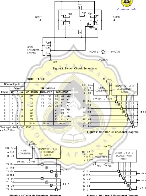
Figure 1. Switch Circuit Schematic
IN/OUT
LEVEL
CONVERTED
CONTROL
VDD
VEE
VDD
VDD
VDD
OUT/IN
VEE
IN/OUT
OUT/IN
CONTROL
TRUTH TABLE
Control Inputs
ON Switches
Inhibit
Select
ON Switches
Inhibit
C*
B
A
MC14051B
MC14052B
MC14053B
0
0
0
0
X0
Y0
X0
Z0
Y0
X0
0
0
0
1
X1
Y1
X1
Z0
Y0
X1
0
0
1
0
X2
Y2
X2
Z0
Y1
X0
0
0
1
1
X3
Y3
X3
Z0
Y1
X1
0
1
0
0
X4
Z1
Y0
X0
0
1
0
1
X5
Z1
Y0
X1
0
1
1
0
X6
Z1
Y1
X0
0
1
1
1
X7
Z1
Y1
X1
1
x
x
x
None
None
None
* Not applicable for MC14052
x = Don’t Care
Figure 3. MC14052B Functional Diagram
Figure 4. MC14053B Functional Diagram
16
VDD
8
VSS 7
VEE
13 X
3 Y
BINARY TO 1–OF–4
DECODER WITH
INHIBIT
LEVEL
CONVERTER
INH 6
A 10
B 9
X0 12
X1 14
X2 15
X3 11
Y0 1
Y1 5
Y2 2
Y3 4
BINARY TO 1–OF–2
DECODER WITH
INHIBIT
LEVEL
CONVERTER
16
VDD
8
VSS 7
VEE
14 X
15 Y
4 Z
INH 6
A 11
B 10
C 9
X0 12
X1 13
Y0 2
Y1 1
Z0 5
Z1 3
Figure 2. MC14051B Functional Diagram
INH 6
A 11
B 10
C 9
X0 13
X1 14
X2 15
X3 12
X4 1
X5 5
X6 2
X7 4
8
VSS 7 VEE
16
VDD
3 X
BINARY TO 1–OF–8
DECODER WITH
INHIBIT
LEVEL
CONVERTER
TEST CIRCUITS
Figure 5.
∆
V Across Switch
Figure 6. Propagation Delay Times,
Control and Inhibit to Output
Figure 7. Bandwidth and Off–Channel
Feedthrough Attenuation
Figure 8. Channel Separation
(Adjacent Channels Used For Setup)
Figure 9. Crosstalk, Control Input to
Common O/I
Figure 10. Off Channel Leakage
CONTROL
SECTION
OF IC
SOURCE
V
ON SWITCH
PULSE
GENERATOR
INH
A
B
C
RL
CL
Vout
VDD VEE VEE VDD
INH
A
B
C
VSS
Vin
RL
CL = 50 pF
Vout
VDD – VEE
2
INH
A
B
C
OFF
ON
RL
RL
CL = 50 pF
Vout
Vin
VDD – VEE
2
INH
A
B
C
R1
RL
CL = 50 pF
Vout
CONTROL
SECTION
OF IC
OFF CHANNEL UNDER TEST
OTHER
CHANNEL(S)
COMMON
VDD
VEE
VEE
VDD
VEE
VDD
NOTE: See also Figures 7 and 8 on Page 6–51.
A, B, and C inputs used to turn ON or OFF
the switch under test.
LOAD
Figure 11. Channel Resistance (RON) Test Circuit
VDD
VEE = VSS
10 k
VDD
KEITHLEY 160
DIGITAL
MULTIMETER
1 k
Ω
RANGE
X–Y
PLOTTER
TYPICAL RESISTANCE CHARACTERISTICS
Figure 12. VDD = 7.5 V, VEE = – 7.5 V
Figure 13. VDD = 5.0 V, VEE = – 5.0 V
R
ON
, “ON” RESIST
ANCE (OHMS)
350
300
250
200
150
100
0
50
– 8.0
– 10
– 6.0 – 4.0 – 2.0
0
0.2
4.0
6.0
8.0
10
Vin, INPUT VOLTAGE (VOLTS)
TA = 125
°
C
25
°
C
– 55
°
C
R
ON
, “ON” RESIST
ANCE (OHMS)
350
300
250
200
150
100
0
50
– 8.0
– 10
– 6.0 – 4.0 – 2.0
0
0.2
4.0
6.0
8.0
10
Vin, INPUT VOLTAGE (VOLTS)
TA = 125
°
C
25
°
C
– 55
°
C
Figure 14. VDD = 2.5 V, VEE = – 2.5 V
R
ON
, “ON” RESIST
ANCE (OHMS)
700
600
500
400
300
200
0
100
– 8.0
– 10
– 6.0 – 4.0 – 2.0
0
0.2
4.0
6.0
8.0
10
Vin, INPUT VOLTAGE (VOLTS)
TA = 125
°
C
25
°
C
– 55
°
C
Figure 15. Comparison at 25
°C, VDD = –VEE
R
ON
, “ON” RESIST
ANCE (OHMS)
350
300
250
200
150
100