A Novel Logic Element for Power Reduction in
FPDs
Thomas Marconi, Koen Bertels, Georgi Gaydadjiev
Computer Engineering Lab
Delft University of Technology
{
thomas,koen,georgi
}
@ce.et.tudelft.nl
Technical Report
CE-TR-2010-01
Abstract
1
Introduction
The advantages of using field-programmable devices (FPDs) are instant manu-facturing turnaround, low start-up costs, low financial risk and ease of design changes [2]. However to get these benefits, the users need to pay the addi-tional costs: higher power consumption (approximately 12x bigger dynamic power), larger silicon areas (40x more required area) and lower operating speeds (3.2x slower) compared to the ASICs [7]. Higher power consumption requires higher packaging cost [3][8][11], shortens chip life-times[3], requires expensive cooling systems[3][8][11], decreases system reliability [11] and prohibits battery operations[3][8][11]. Therefore, it is a critical to reduce the FPDs power con-sumption.
Many techniques have been proposed for power reduction in FPDs. How-ever, all existing techniques to reduce power still target what we call a ”conven-tional logic element”. This conven”conven-tional logic element (LE) has been used by researchers of FPDs since it was patented by Birkaner and Chua in 1978 [1]. Al-though FPDs have been improved significantly since the original proposal, they still make use of a proposal dated 1978 that may need to be reconsidered. The conventional LE contains the combinational logic (e.g. the lookup table LUT in FPGAs) and the storage element (D flip-flop). The output of the combina-tional logic is connected to the input of the storage element; the clock input of D flip-flop (DFF) is connected to the clock signal. Since the DFF clock input is connected directly to the clock signal, the DFF is always clocked even when it is not necessary. For example, whenD=Q, the DFF does not need to be clocked. This unnecessary transition wastes power in FPDs using the conventional LEs. This is related to the fact that even low-power flip-flops consume power during logic transition from zero-to-zero and from one-to-one as shown in [102].
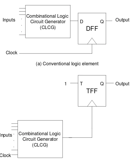
To solve this problem, we propose a novel LE for reduced FPDs power con-sumption. The proposed LE can be used in any kinds of FPDs: Simple PLDs (SPLDs), Complex PLDs (CPLDs) as well as Field-Programmable Gate Arrays (FPGAs). The differences between our LE and the conventional LE are in the type of flip-flops and the internal organization. Instead of using D flip-flops, we use T flip-flops with input T at logic one (T=1). This is related to the fact that designing sequential circuits using TFFs is more power efficient than DFFs as reported in [101]. Instead of connecting the output of the combinational logic to the input of the FF, we connect the output of the combinational logic to the clock input of the FF. As a result, the LE has an ability to not propagate unnecessary clock transitions without any additional clock gating controller.
to stop clock activity, additional power and area are also saved.
In conventional LEs, the FF is ready to be clocked when the input D has a stable logic value from the output of the combinational logic determined by the FF setup time. In our LEs, since the input T of the FF is always in logic one, the FF is always ready to be clocked. As a consequence, logic circuits implemented using our LEs can be clocked faster than logic circuits using conventional LEs. The Microelectronic Center of North Carolina (MCNC) benchmark circuits [4] are used to evaluate FPDs using proposed LEs compared to FPDs targeting conventional LEs in 45 nm BSIM4 CMOS technology [6]. We use LTSPICE tools [5] for transistor-level circuit simulations with nominal supply voltage VDD of 1.2. The evaluation is performed in terms of total power, logic power, clock power, interconnect power, dynamic power, static power, speed, and area. The main contributions of this report are:
• a novel low power LE for FPDs;
• up to 42 % of total power reduction for the MCNC benchmarks by avoiding unnecessary activities: clock, logic, and interconnect;
• up to 33 % performance improvement due to the ”always ready” flip-flops. The remainder of this report is organized as follows. In Section 2, we give a review of related work in reducing power for FPDs. Our proposed LE to reduce power is presented in Section 3. In Section 4, we evaluate our proposed LE. Finally, in Section 5, we summarize the report.
2
Related work
Modern FPGAs contain embedded hardware blocks, such as: multipliers, DSPs, and memories. It is reported in [7] [18] that by mapping designs to these blocks can reduce power consumption. The design that uses hard blocks requires less interconnection. As a result, static and dynamic power consumptions are re-duced.
Adding programmable delay circuits into configurable logic blocks is reported in [25] to reduce power consumption in FPGAs. The generation of glitches is avoided by aligning the arrival times of signals using the proposed programmable delay circuits. As a result, the glitched are reduced for minimizing dynamic power consumption.
To reduce dynamic power consumption in FPGAs, circuits are pipelined in [21] [22] [23]. This technique reduces the number of levels of the circuit between registers by dividing the circuit into stages. A circuit with lower levels tends to produce fewer glitches. Since a circuit with fewer glitches consumes less dynamic power, the power consumption is reduced.
Retiming can be used to reduce dynamic power consumption in FPGAs [24]. The idea is to redistribute registers along a signal path without changing the functionality of the circuit. By doing so, the logic between registers is minimized, hence reducing glitches. As a result, the dynamic power consumption is reduced. The bit-widths of the internal signals of circuits can be optimized to reduce dynamic power consumption. A circuit with shorter bit-widths consumes less power. This approach applied in FPGAs is reported in [29] [30].
Clock gating is used to reduce dynamic power consumption by selectively blocking the circuit local clock when no state or output transition takes place. The clock gating controller is needed for detecting the conditions of the observed circuit. Based on these conditions, the clock gating controller can know the exact time when it can stop clock signal to be transported to the specific circuit for power saving. It is used in FPGAs [31] [32] [33] [34] [18] [35] [36] [37] and CPLDs [38]. This technique is supported by commercial CAD tools from Xilinx as reported in [34]. In [37], an asynchronous FPGA with clock gating is proposed.
Powering FPGAs with variable supply voltage can also be used to reduce power consumption [39]. This method is referred as dynamic voltage scaling (DVS). Since there is a quadratic relationship between supply voltage and dy-namic power, reducing the voltage will significantly reduce the dydy-namic power. Moreover, a cubic relationship between supply voltage and leakage power re-duces significantly the leakage power.
Modern FPGAs have the ability to reconfigure part of their resources with-out interrupting the remaining resources at runtime. Hardware sharing can be realized by utilizing this partial reconfiguration feature for power consumption reduction . Power saving using this approach in FPGAs is reported in [103] [104] [105] [106] [18] [40] [41].
Clock scaling is an approach to reduce power consumption by adjusting operating clock frequency dynamically. Applying this approach in FPGAs is reported in [42].
A lower threshold voltage transistor runs faster, but it consumes more power. Multi-threshold voltage technique is to use higher threshold voltage transistors on noncritical paths to reduce static power, and low threshold voltage transistors on critical paths to maintain performance. This technique has been applied in commercial FPGAs as reported in [18] [43].
A lower capacitive circuit consumes less dynamic power. One of the ways to reduce capacitance is to use a low-k dielectric material. This technique is used by commercial FPGAs as shown in [18] [43].
A simple way to reduce both static and dynamic power is to scale down the supply voltage. This has been applied in commercial FPGAs as reported in [18] [43].
Building circuits with bigger size lookup tables (LUTs) needs less intercon-nection between LUTs. As a result, interconnect power consumption is reduced. This has triggered commercial FPGAs vendors to use bigger size LUTs as re-ported in [18] [20].
turning off circuits that are not in use. It is applied in FPGAs [44] [45] [46] [47] [48]. This technique is used in commercial products, such as: Atmel PLDs [50], Altera CPLDs [51], Actel FPGAs [52], QuickLogic FPGAs [53], Xilinx FPGAs [18] , Altera FPGAs [49]. In [45], an asynchronous FPGA with autonomous fine-grain power gating is proposed. How to partition a design to better benefit from power gating technique is reported in [48].
Conventional single-edge-triggered flip-flops respond only once per clock pulse cycle. To reduce power consumption, a flip-flop that can respond to both the positive and the negative edge of the clock pulse (double-edge-triggered flip-flops) was proposed in [54]. This technique is used in Xilinx CPLDs to reduce power consumption [55].
Since SRAM memory is volatile, SRAM-based FPGAs need to be recon-figured before usage. This reconfiguration consumes power. In contrast, the flash-based FPGAs (e.g. Actel FPGA [52]) that use non-volatile memory can be operated directly without reconfiguration.
Powering FPGAs with two different supply voltages (dual-Vdd) can also re-duce power consumption as reported in [8] [56] [57] [58] [59] [60]. It is to use lower supply voltage on noncritical paths to reduce power, and higher supply voltage on critical paths to maintain performance. Algorithms for Vdd assign-ment are presented in [58] [59]. [60] combines concurrently this technique with retiming to better reduce power consumption in FPGAs.
Reordering input signals to LUTs can reduce dynamic power consumption in FPGAs. By doing so, we can minimize the switching activity inside LUTs as reported in [61]. Since power consumption depends linearly on switching activity, reducing this results in power consumption improvement.
Power consumption in FPGAs can be reduced by dividing a finite state ma-chines (FSM) into two smaller sub-FSMs using a probabilistic criterion [62]. The idea is to activate only one sub-FSM at a time, meanwhile the other is disabled for power reduction. Choosing state encoding of FSMs for power reduction in FPGAs is reported in [63] [64]. The idea is to minimize the bit changes during state transitions for reducing switching activity, hence minimizing the dynamic power consumption.
Using a diagonally symmetric interconnect pattern in Virtex-5 FPGAs can reduce number of interconnect routing hops as reported in [65]. As a result, the interconnect power consumption is reduced.
Since not all inputs of LUTs are used in real FPGA designs, leakage power can be reduced by shutting off SRAM cells and transistors associated with unused LUT inputs as reported in [11].
Using LUTs that have an ability to operate in two different modes (high-performance and low-power) can be used for leakage power reduction as reported in [66]. The idea is to use some transistors for lowering supply voltage across input inverters of LUTs during low power operation mode. Since not all LUTs need to be operated in high-performance mode, the leakage power is reduced.
technique for leakage power reduction in FPGAs is reported in [67].
Since leakage power in multiplexers is dependent on their input states, se-lecting polarities for logic signals (i.e. inverted or not) so that the multiplexers are operated in low-leakage states in the majority of time can be used to reduce leakage power in FPGAs [68]. To reduce more leakage power, the work in [68] is extended by [69]. In [69], not only polarity is considered to achieve low leakage states, but also the order of input signals to LUTs is modified to have a better leakage power reduction. It is different from [61] that targets dynamic power, the work in [69] targets static power by reordering input signals to LUTs. Since the leakage power is state dependent [70], changing this state results leakage power reduction.
Redesigning routing switches can be used to reduce overall power consump-tion in FPGAs. Routing switches that can operate in three different modes: high-speed, low-power or sleep is reported in [71]. Using dual-Vdd-dual-Vt routing switches for reducing interconnect power is presented in [72]. Applying dual-vdd and power gating techniques for routing switches is proposed in [73].
A circuit in high-level synthesis(HLS) can be implemented by combining functional units, such as: multipliers, adders, multiplexers, etc. Each functional unit can be realized using one of varied implementations. Each implementation requires a certain area and runs at a specific speed with required power con-sumption. To reduce power consumption, we need to choose the best design for a given circuit that can meet timing requirement with minimal power. HLS algorithms for minimizing power consumption in FPGAs are reported in [74] [75].
Logic synthesis in FPGAs is a process of transforming a given design (coded in schematic or HDL) into a gate-level circuit. Considering switching activity during logic synthesis for FPGAs to reduce power consumption is presented in [76]. The idea is to minimize switching activity during logic synthesis. As a result, the power consumption is reduced.
Technology mapping in FPGAs is a process of transforming a given circuit into a circuit that only consists of LUTs. The way we map circuits into FPGAs can affect the power consumption. The algorithms to perform this process for power reduction are presented in [77] [78] [79] [80] [81]. The main idea is to pack nodes with high switching activity inside LUTs. By doing so, we can minimize power needed to transport signals of nodes among LUTs. To better estimate the switching activity, glitches are considered during technology mapping in [27].
Transformation by changing the functionalities of LUTs with rerouting [82] and without rerouting [83] can be used to reduce power consumption in FPGAs. [82] performs the transformation after technology mapping by reducing switch-ing densities of the outputs of the LUTs, whereas [83] transforms the design after mapping, placement, and routing by considering switching activity and capacitance at the outputs of the LUTs.
can affect the power consumption. The clustering algorithms to reduce power consumption are presented in [85] [86]. The main idea in [85] is to minimize intercluster connections for reducing interconnection power. Clustering for FP-GAs with dual-Vdd is shown in [86]. Assigning noncritical paths to clusters with low power supply voltage is the key idea of [86].
Placement algorithms to reduce power consumption in FPGAs are presented in [87] [88] [89]. The main idea is to add estimated dynamic power into cost function of the placement algorithms. As a result, dynamic power is reduced during placement. A placement algorithm that takes into account the cost of using clock network resources to reduce power consumed by clock network is reported in [89].
Routing algorithms to reduce power consumption in FPGAs are reported in [87] [26]. Assigning nodes with high switching activity to low-capacitance routing resources is the main idea behind the routing algorithm for reducing interconnect power in [87]. A routing that can balance arrival times of the inputs of the same LUTs to reduce power consumption in FPGAs is proposed in [26]. By doing so, the glitches are reduced. As a result, the dynamic power consumption is minimized.
Combining power-aware technology-mapping, clustering, placement, and rout-ing algorithms to reduce power consumption in FPGAs is reported in [90].
To reduce power during runtime reconfiguration, configuration memory with two different types of memories [91] or runtime configurable memory with two different modes [92] is proposed. One type(mode) is optimized for high speed operation; whereas the other type(mode) is optimized for low power operation. Tasks that do not require high speed reconfiguration can be reconfigured to the low power one for power saving during reconfiguration.
Some signals in a digital circuit do not affect an output of the circuit for cer-tain conditions. Stopping these signals to flow to the circuit at those conditions for dynamic power saving in FPGAs is reported in [93] [94].
Choosing the best operating mode for each memory on FPGAs based on prior knowledge of its dead intervals is reported in [95] to reduce leakage power consumption. The memory can be operated in three operating modes: active, drowsy, and sleep. The sleep mode is a condition when the power supply is disconnected to the memory; whereas the drowsy mode is a condition when the memory is connected to a lower supply voltage. The idea is to operate the memory based on its dead intervals. The memory with long/medium/short dead interval is operated on sleep/drowsy/active mode.
Constraining designs to be implemented on the specific regions within the FPGA to minimize power consumed by clock networks is reported in [96]. The idea is to place logic closer together for minimizing the clock network usage. As a result, the FPGA power consumption is reduced.
Older generation FPGAs use dual-oxide process technology: thick oxide transistors (slow transistors) for I/Os and thin oxide transistors (fast transistors) for core. To reduce leakage power in FPGAs, triple-oxide process technology is used in modern FPGAs (e.g. Virtex-4) [19] [18]. In these FPGAs, another type of transistors with medium thickness oxide is dedicated for the configuration memory and interconnect pass gates.
The leakage power consumed by an asymmetric SRAM cell depends on its stored data. Since 87 % of the configuration memory cells in FPGAs store logic zero in the real FPGA design [107], using asymmetric SRAM cells with low leakage at logic zero for FPGAs to reduce leakage power consumed by reconfiguration memory is reported in [107]. The idea is to select polarities for logic signals (i.e. inverted or not) that can increase the number of zeros stored on the configuration memory. Since the number of zeros is increased, the number of memory cell that operates at low leakage is increased. As a result, the leakage power consumed by the reconfiguration memory is reduced.
To reduce interconnect power, low-voltage swing interconnects are applied for FPGAs in [108] [109]. Since the dynamic power consumption is linearly proportional to the voltage swing, interconnect power is reduced by minimiz-ing the voltage swminimiz-ing on interconnects. Because this technique degrades the performance, in [108], the dual-edge triggered flip-flops are used to handle this degradation. Applying low swing interconnects only on non-critical paths is proposed in [109] to reduce the performance degradation of this technique.
Although many techniques presented above have been proposed for power reduction in field-programmable devices (FPDs), all of them still use a conven-tional LE as a basic building block. This convenconven-tional LE has been used by FPDs since it was patented by Birkaner and Chua in 1978 [1].
3
Our Low Power Logic Element(LE)
The purpose of LEs in FPDs is to provide the basic programmable combina-tional logic and storage elements used in digital logic systems. A LE contains a combinational logic circuit generator (CLCG) and a storage element as shown in Figure 1. The CLCG is used for the combinational function, while the storage element is used for saving temporary results.
In conventional LEs, the output of CLCG is connected to the input of the storage element as illustrated in Figure 1(a). The storage element in the con-ventional LE is a D Flip-flop (DFF). Since the clock input of DFF is connected to the clock signal, the DFF is always clocked. When the D input of DFF has a different value compared to its output Q (D̸=Q), the DFF needs to be clocked for updating the storage data as presented in Figure 2(a). Otherwise, when
D = Q, the DFF does not need to be clocked. This unnecessary transition wastes power in the conventional LEs.
Combinational Logic Circuit Generator
(CLCG)
D Q
Clock
Output Inputs .
.
.
Combinational Logic Circuit Generator
(CLCG)
T Q
Clock
Output
Inputs.
.
.
1
(a) Conventional logic element
(b) Our logic element
DFF
TFF
Figure 1: Logic elements
is controlled by the clock gating controller as shown in Figure 2(b). The clock gating controller blocks the clock signal for reaching DFFs clock inputs when the DFFs should not be clocked (D =Q). As a result, the unnecessary clock transitions can be avoided for power saving. The drawback of clock gating is the need of additional controllers that consume additional area and power. To reduce this overhead, the controller usually does not control an individual FF, but it controls a group of FFs together. As a result, the clock gating cannot stop all unnecessary clock transitions.
CLCG 0 DFF 0->0 (a) Conventional logic element without clock gating
CLCG 0 DFF 0->0
(b) Conventional logic element with clock gating (no unnecessary clock)
CLCG
(c) Our logic element (no unnecessary clock)
Figure 2: Basic operations of logic elements
of the inputs of the LUT is used for feeding the clock signal, the LUT capacity is decreased. This will not be a problem, since not all inputs of LUTs are used in real FPGA designs as reported in [11], we can use these unused inputs for free to feed the clock signal.
The benefits of our LE are avoiding unnecessary clock transitions and no additional clock gating controller as shown in Figure 2(c). The CLCG avoids clock transitions to be propagated to an individual FF when the state of the FF will not change. As a result, the unnecessary clock transitions are totally avoided and hence power is reduced. Additional power and area are also saved in comparison to the clock gating approach, since the additional controller is not needed.
unified path approach.
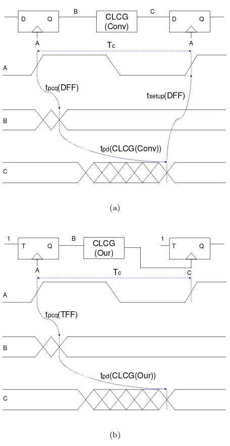
Running faster than the conventional one is another benefit of using our LEs in FPDs. The FF can be clocked properly if its input is stable at least before its setup time. In conventional LE, the input value of the DFF is not constant; it depends on the output of the connected CLCG. In our LE, since the T input of the TFF is constant (T = 1), the TFF is always ready to be clocked. As a consequence, logic circuits implemented using our LEs can be clocked faster than logic circuits using conventional LEs.
The timing diagrams of circuits using our LEs compared to the conventional LEs are presented in Figure 3. In this figure,tpcq(DF F) is the clock-to-Q propa-gation delay of DFF;tpd(CLCG(Conv)) is the propagation delay of conventional CLCG;tpd(CLCG(Our)) is the propagation delay of our CLCG;tsetup(DF F) is the setup time of DFF; tpcq(T F F) is the clock-to-Q propagation delay of TFF. From this figure, we can obtain the clock period of the circuit using con-ventional LEs as Tc(Conv) ≥tpcq(DF F) +tpd(CLCG(Conv)) +tsetup(DF F)
Replacing some flip-flops with latches can speedup circuits up to 19 % [99], reduce circuit area up to 22 % [98] and reduce power consumption up to 73 % [98]. Not all flip-flops can be replaced by latches. This replacement can be done if only if there is no transparency issue between the input and output of the flip-flop. The improvement using this replacement depends on the number of flip-flops that can be replaced by latches. Since the input of flip-flop in our LE is constant (T = 1), the transparency between the input and output of the flip-flop is not an issue anymore. As a result, replacement of flip-flip-flops by latches is easily applicable. By doing so, we can obtain additional power efficiency, lower area, and faster designs.
CLCG (Conv)
D Q D Q
A A
B C
A
B
C
tpcq(DFF)
tpd(CLCG(Conv))
tsetup(DFF)
Tc
(a)
CLCG (Our)
T Q T Q
C A
1 B
A
B
C
tpcq(TFF)
tpd(CLCG(Our)) 1
Tc
(b)
4
Evaluation
4.1
Experimental setup
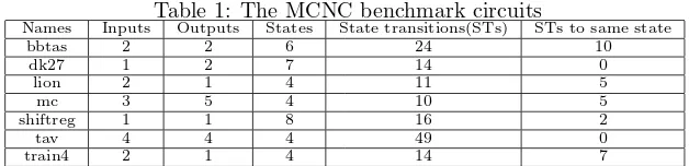
To evaluate the proposed LE, transistor-level circuit simulations were performed using LTSPICE tools [5] and 45 nm BSIM4 CMOS device models [6] with nom-inal VDD of 1.2. Since transistor-level simulations are used, glitches are au-tomatically taken into account. The MCNC benchmark circuits [4] were used for our study. Since our proposal is new, no CAD tools (high level synthesis, technology mapping, place and route tools) are available for targeting FPDs using the proposed LE. For that reason, we performed all design steps by hand. This is also why we did not evaluate our proposal with all MCNC benchmark circuits; we only evaluated the proposal with the MCNC benchmark circuits that were not too complex for hand design as shown in Table 1. Since our pro-posal can save power only for circuits with storage elements, we only evaluate our proposal based on MCNC benchmark circuits using storage.
Table 1: The MCNC benchmark circuits
Names Inputs Outputs States State transitions(STs) STs to same state
bbtas 2 2 6 24 10
Since the values of SRAM cells remain constant after configuration (no ad-ditional dynamic power) and there is no difference in the number of SRAM cells for FPDs using the conventional and our LEs (same additional static power), we do not model them in our experiments. We connect the internal signals directly to VDD or ground depending on their contents. The ratio between the transistor widths of nMOS tansistors and pMOS transistors in our experimental circuits is Wp
Wn = 3 to model worst case in terms of leakage power. To accurately
model LUTs, multiplexers, and routing circuits, we selected transmission-gate based implementation as used by Xilinx commercial FPGAs patented in [100]. In this experiment, we assume unused resources can be turned off to model power gating both for the conventional FPDs and our proposal.
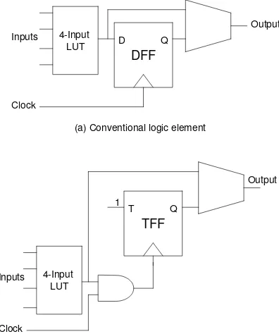
First, we created experimental LE circuits both for the conventional and our proposed LEs. The experimental LEs are presented in Figure 4. In this experi-ment, an additional AND gate for feeding clock signal was used to make manual implementation of the MCNC circuits easier. An experimental conventional LE consists of a 4-Input LUT, a DFF, and an output multiplexer as illustrated in Figure 4(a); while the proposed one consists of a 4-Input LUT, a TFF, an output multiplexer, and an AND gate as shown in Figure 4(b). These two LE circuits will be used for creating experimental FPD circuits.
pro-4-Input
LUT D Q
Clock
Output Inputs
T Q
Output
Clock Inputs
1
(a) Conventional logic element
(b) Our logic element DFF
TFF
4-Input LUT
Figure 4: Experimental logic elements
grammable switches) were used for connecting needed LE circuits which will be used for creating benchmark circuits.
Finally, we implemented each MCNC benchmark circuit onto the FPDs using conventional LEs and our LEs. MCNC circuits in Berkeley Logic Interchange Format (BLIF) mapped for 4-input-LUT-based FPDs were used for implement-ing circuits onto the FPD based on conventional LEs. We manually implemented each MCNC benchmark circuit onto the FPD circuit using the proposed LEs. In this step, we computed all of the functions needed for the LUTs in the new LEs which are totally different from the functions of the conventional approach. After that, we placed the computed functions onto LUTs of the FPD using our proposed LEs and made needed interconnections for each MCNC circuit by reconfiguring the FPD. The reconfigurations were done by modifying the functionalities of the 4-Input LUTs, the output multiplexes, and the intercon-nections.
were found to work properly. The test vectors were chosen to represent all combinations of input values.
The benchmark circuits were simulated to obtain the needed performance parameters: power, speed, and area for each benchmark circuit. Area is in terms of number of transistors required to implement the benchmark circuit using FPD circuits. The breakdowns of total power which consists of logic power (total power inside LEs), clock power, and interconnect power were also obtained. To complete the power evaluation, we also analyzed the static and dynamic powers. The evaluation was conducted at 500 MHz clock speed.
4.2
Experimental results
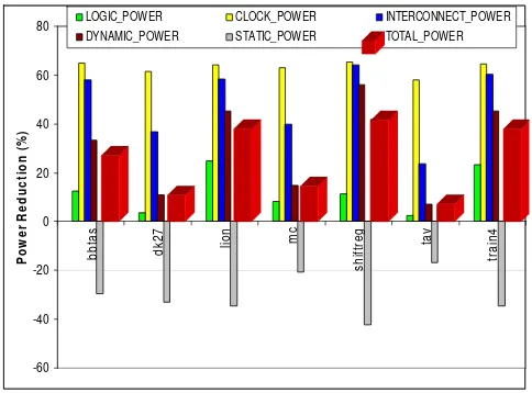
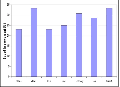
The experimental results of power consumption both for an FPD using conven-tional LEs and an FPD using our LEs are depicted in Table 2 and Table 3. The power reductions of an FPD using proposed LEs compared to an FPD using conventional LEs as presented in Figure 5 were computed based on the results from Table 2 and Table 3. Besides power evaluations, we also evaluate the area overhead of the FPD using our proposed LEs compared to the FPD using con-ventional LEs as shown in Figure 6. Moreover, the performance improvement was also evaluated and is shown in Figure 7.
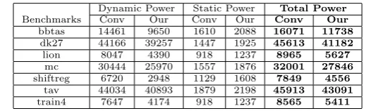
Table 2: Experimental results of Logic Power, Clock Power, and Interconnect Power (µW)
Logic Power Clock Power Interconnect Power Benchmarks Conv Our Conv Our Conv Our
bbtas 11357 9925 2320 811 2394 1002 dk27 39105 37642 2320 891 4188 2649 lion 5943 4460 1515 540 1507 627
mc 28204 25913 1515 559 2282 1374 shiftreg 3361 2975 2317 804 2171 777
tav 40505 39480 1522 641 3886 2970 train4 5576 4287 1514 538 1475 586
Table 3: Experimental results of Dynamic Power, Static Power, and Total Power (µW)
Dynamic Power Static Power Total Power
Benchmarks Conv Our Conv Our Conv Our
bbtas 14461 9650 1610 2088 16071 11738
dk27 44166 39257 1447 1925 45613 41182
lion 8047 4390 918 1237 8965 5627
mc 30444 25970 1557 1876 32001 27846
shiftreg 6720 2948 1129 1608 7849 4556
tav 44034 40893 1879 2198 45913 43091
train4 7647 4174 918 1237 8565 5411
-60
Figure 5: Power Reduction (%)
has up to 25 % less logic power compared to the FPD using conventional LEs. Because of less activity, the interconnect activity among LEs is also reduced. As a consequence, the FPD using proposed LEs has up to 64 % less interconnect power compared to the FPD using conventional LEs.
The FPD using our proposed LEs reduces up to 56 % dynamic power com-pared to the FPD using conventional LEs by avoiding unnecessary activities: clock, logic, and interconnect as presented in Figure 5. Since the proposed ex-perimental LE has an additional AND gate, the FPD has up to 42 % higher static power as shown in Figure 5 and up to 7 % bigger area compared to the FPD using conventional LEs as presented in Figure 6. Since not all inputs of LUTs are used in real designs as reported in [11], we can use these unused inputs to feed the clock signal. In this case, we do not need the additional logic level (the AND gate) for feeding the clock signal anymore.
Although the FPD using our LEs consumes more static power than the FPD using conventional elements, the overall power consumption of the FPD using our proposal is still less than the conventional one as shown in Figure 5. Since the impact of increasing in static power is lower than the impact of reducing the clock, logic, and interconnect powers, the FPD using our proposed LEs still can reduce up to 42 % total power compared to the FPD using conventional LEs as shown in Figure 5.
Circuits that go to the same state do not need to be clocked for power saving is the basic idea of our approach. This means that we can get more power reduction if the circuits frequently go to the same state. As shown in Table 1, the state of the storage elements in the dk27 and tav benchmark circuits never goes to the same state. As a result, the total power reduction for these benchmark circuits is smaller compared to other benchmark circuits.
0
bbtas dk27 lion mc shiftreg tav train4
A
Figure 6: Area Overhead (%)
0
bbtas dk27 lion mc shiftreg tav train4
S
the input D is ready before the needed setup time for the FF to work properly. In contrast, the TFF in our LE is always ready to receive clock signal since the input T of its TFF is always ready at logic one. As a result, the FPD using proposed LEs runs up to 33 % faster than the FPD using conventional LEs as shown in Figure 7.
Table 4 shows the comparison between our solution and clock gating solu-tions. Clock gating results are obtained from the original papers: [31], [32], and [33]. This table shows that our proposal saves more power than clock gating solutions. Moreover, our proposal generates faster designs than clock gated de-signs. The area cannot be directly compared due to limited information in the related papers.
Table 4: Comparison with clock gating solutions
Evaluation Our solution Clock Gating solutions
[31] [32] [33]
Total power reduction 6 - 42 % 5 - 33 % 6.2 - 7.7 % 1.8 - 27.9 % Speed 23-33 % faster Not available 0 - 2 % slower 1.1 % faster Area 2 - 7 % overhead Not available Not available Not available
5
Conclusions
In this report, we have proposed a novel low power logic element(LE) to replace the conventional LE. Since unnecessary clock transitions are avoided, the clock power is reduced by up to 65 %. By avoiding unnecessary clock transitions, the activity inside the proposed LEs is also reduced. As a result, the FPD using the proposed LEs consumes up to 25 % less logic power compared to the FPD using conventional LEs. Because of activity reduction, the LEs interconnect power is also reduced by up to 64 % compared to the FPD using conventional LEs. Moreover, since we do not need an additional controller to stop clock activity, additional power and area are reduced in comparison to clock gating approach. In our LE, since the input T of the FF is always in logic one, the FF is always ready to be clocked. As a consequence, the FPD using our proposed LEs not only consumes up to 42% less total power by avoiding unnecessary activities: clock, logic, and interconnect, but also it runs up to 33% faster than the FPD using conventional LEs because of its ”always ready” flip-flops.
Some directions for future research are: (1) CAD tools development for FPDs using the proposed LEs, (2) investigation of circuits using latches or hybrid latches and flip-flops for FPDs.
Acknowledgment
References
[1] J. M. Birkner and H-T. Chua, ”Programmable Array Logic Circuit,” US Patent No. 4124899, 1978.
[2] S. Brown and J. Rose, ”Architecture of FPGAs and CPLDs: A Tutorial,” IEEE Design and Test of Computers, Vol. 13, No. 2, pp. 42-57, 1996. [3] E. I. Boemo , G. G. de Rivera , S. L´opez-Buedo , J. M. Meneses, ”Some
Notes on Power Management on FPGA-Based Systems,” Proceedings of the 5th International Workshop on Field-Programmable Logic and Appli-cations, pp. 149-157, 1995.
[4] S. Yang, ”Logic Synthesis and Optimization Benchmarks User Guide Ver-sion 3.0,” Technical Report, Microelectronic Center of North Carolina (MCNC), 1991.
[5] http://www.linear.com/designtools/software/ [6] http://www.eas.asu.edu/ ptm/latest.html
[7] I. Kuon and J. Rose, ”Measuring the Gap between FPGAs and ASICs,” Proceedings of the 2006 ACM/SIGDA 14th international symposium on Field programmable gate arrays, Monterey, California, USA, pp. 21-30, 2006.
[8] A. Gayasen, K. Lee, V. Narayanan, M. Kandemir, M. J. Irwin, T. Tuan, ”A Dual-Vdd Low Power FPGA Architecture,” Proceedings of the Inter-national Conference on Field-Programmable Logic and its applications, pp. 145157, August 2004.
[9] R. Mukherjee , S. Ogrenci Memik, ”Evaluation of Dual VDD Fabrics for Low Power FPGAs,” Proceedings of Asia and South Pacific Design Au-tomation Conference, pp. 1240-1243, January 2005.
[10] F. Li , Y. Lin , L. He , J. Cong, ”Low-power FPGA using Pre-defined Dual-Vdd/dual-Vt Fabrics,” Proceedings of ACM/SIGDA international sympo-sium on Field programmable gate arrays, pp. 42-50, February 2004. [11] S. Mondal and S. O. Memik, ”Fine-grain Leakage Optimization in SRAM
based FPGAs,” Proceedings of the ACM Great Lakes Symposium on VLSI, pp. 238-243, 2005.
[12] Atmel, ”Saving Power with Atmel PLDs,” 2000.
[13] Lattice Semiconductor, ”Practical Low Power CPLD Design,” August 2009. [14] Xilinx, ”Low Power Design with CoolRunner-II CPLDs,” XAPP377, May
[15] Altera, ”Power Management in Portable Systems Using MAX II CPLDs,” Application Note 422, July 2006.
[16] Actel, ”Total System Power: Evaluating The Power Profile of FPGAs,” 2008.
[17] QuickLogic, ”Minimizing Energy Consumption with Very Low Power Mode in PolarPro Solution Platform CSSPs,” Application Note 88, 2008. [18] M. Klein, ”Power Consumption at 40 and 45 nm,” Xilinx WP298, April
2009.
[19] P. Abusaidi, M. Klein, and B. Philofsky, ”Virtex-5 FPGA System Power Design Considerations,” Xilinx WP285 (v1.0) February 14, 2008.
[20] Altera, ”FPGA Architecture,” WP-01003, July 2006.
[21] S.J.E. Wilton, S.S. Ang, and W. Luk, ”The Impact of Pipelining on Energy per Operation in Field Programmable Gate Arrays,” Proceedings of Field Programmable Logic and Applications, LNCS 3203, pp. 719-728, 2004. [22] S. Bard and N. I. Rafla, ”Reducing Power Consumption in FPGAs by
Pipelining,” Proceedings of Circuits and Systems, pp. 173-176, 2008. [23] N. Rollins and M. J. Wirthlin, ”Reducing Energy in FPGA Multipliers
through Glitch Reduction,” Proceedings of International Conference on Military Applications of Programmable Logic Devices, pp. 1-10, September 2005.
[24] R. Fischer, K. Buchenrieder, and U. Nageldinger, ”Reducing the Power Consumption of FPGAs through Retiming,” Proceedings of the Interna-tional Conference and Workshops on Engineering of Computer-Based Sys-tems, pp.89-94, April 2005.
[25] J. Lamoureux, G.G. Lemieux, and S.J.E. Wilton, ”GlitchLess: Dynamic Power Minimization in FPGAs through Edge Alignment and Glitch Filter-ing,” Transactions on Very Large Scale Integration Systems (TVLSI), Vol. 16, No. 11, pp. 1521-1534, 2008.
[26] Q. Dinh, D. Chen, and M.D.F. Wong, ”A Routing Approach to Reduce Glitches in Low Power FPGAs,” Proceedings of IEEE/ACM International Symposium on Physical Design, pp. 99-106, March 2009.
[27] L. Cheng, D. Chen, and M.D.F. Wong, ”GlitchMap: An FPGA Technol-ogy Mapper for Low Power Considering Glitches,” Proceedings of Design Automation Conference, pp. 318-323, June 2007.
[29] A. A. Gaffar, J. A. Clarke, and G. A. Constantinides, ”PowerBit - Power Aware Arithmetic Bit-width Optimization,” Proceedings of IEEE Interna-tional Conference on Field Programmable Technology, pp. 289-292, Decem-ber 2006.
[30] G. Constantinides, ”Word-length Optimization for Differentiable Nonlinear Systems,” ACM Trans. on Design Automation of Electronic Sys., Vol. 11, No. 1, pp. 26-43, 2006.
[31] Y. Zhang, J. Roivainen, and A. M¨ammel¨a, ”Clock-Gating in FPGAs: A Novel and Comparative Evaluation,” Proceedings of EUROMICRO Con-ference on Digital System Design, pp.584-590, 2006
[32] S. Huda, M. Mallick, and J.H. Anderson, ”Clock Gating Architectures for FPGA Power Reduction,” Proceedings of IEEE International Confer-ence on Field-Programmable Logic and Applications (FPL), pp. 112-118, Prague, Czech Republic, 2009.
[33] Q. Wang, S. Gupta, and J.H. Anderson, ”Clock Power Reduction for Virtex-5 FPGAs,” Proceedings of ACM/SIGDA International Conference on Field Programmable Gate Arrays (FPGA), pp. 13-22, Monterey, CA, February 2009.
[34] F. Rivoallon, ”Reducing Switching Power with Intelligent Clock Gating,” Xilinx WP370 (v1.1), July 2010.
[35] Actel, ”Dynamic Power Reduction in Flash FPGAs,” Application Note AC323, March 2009.
[36] M. Khan, ”Power Optimization in FPGA Designs,” Altera, 2006.
[37] Achronix, ”Introduction to Achronix FPGAs,” WP001 Rev.1.6, August 2008.
[38] Lattice Semiconductor, ”Practical Low Power CPLD Design,” August 2009. [39] C.T. Chow, L.S.M. Tsui, P.H.W. Leong, W. Luk, and S. Wilton, ”Dynamic Voltage Scaling for Commercial FPGAs,” Proceedings of IEEE Int. Conf. on Field Prog. Technology, pp.215-222, 2005.
[40] C. Kao, ”Benefits of Partial Reconfiguration,” Xilinx, 2005.
[41] J. Becker, M. H¨ubner and M. Ullmann, ”Run-Time FPGA Reconfigura-tion for Power-/Cost-Optimized Real-time Systems,” Proceedings of Inter-national Conference on Very Large Scale Integration of System on Chip, pp. 119-132, December 2003.
[43] C. Jenkins and P. Ekas, ”Low-power Software-defined Radio Design using FPGAs,” Altera, 2006.
[44] A. Rahman, S. Das T. Tuan, and S. Trimberger, ”Determination of Power Gating Granularity for FPGA Fabric,” Proceedings of Custom Integrated Circuits Conference, pp. 9-12, Sept 2006.
[45] S. Ishihara, M. Hariyama, and M. Kameyama, ”A Low-power FPGA based on Autonomous Fine-grain Power-gating,” Proceedings of the 2009 Asia and South Pacific Design Automation Conference, pp. 119-120, 2009. [46] P. S. Nair, S. Koppa, and E. B. John, ”A Comparative Analysis of
Coarse-grain and Fine-Coarse-grain Power Gating for FPGA Lookup Tables,” Proceed-ings of IEEE International Midwest Symposium on Circuits and Systems, pp.507-510, 2009
[47] A. Gayasen, Y. Tsai, N. Vijaykrishnan, M. Kandemir, M. J. Irwin, and T. Tuan, ”Reducing Leakage Energy in FPGAs using Region-constrained Placement,” Proceedings of the International Symposium on Field Pro-grammable Gate Arrays, pp. 51-58, 2004.
[48] H. Hassan, M. Anis, A. El, and D.M. Elmasry, ”Activity Packing in FPGAs for Leakage Power Reduction,” Proceedings of Design, Automation and Test in Europe, pp.212-217, 2005.
[49] M. Khan, ”Power Optimization Innovations in 65-nm FPGAs,” Altera, March 2007.
[50] Atmel, ”Saving Power with Atmel PLDs,” 2000.
[51] Altera, ”Power Management in Portable Systems Using MAX II CPLDs,” Application Note 422, July 2006.
[52] Actel, ”Total System Power: Evaluating The Power Profile of FPGAs,” 2008.
[53] QuickLogic, ”Minimizing Energy Consumption with Very Low Power Mode in PolarPro Solution Platform CSSPs,” Application Note 88, 2008. [54] S.H. Unger, ”Double-edge-triggered Flip-flops,” IEEE Trans. Computers,
Vol. C-30, No. 6, pp. 447-451, June 1981.
[55] Xilinx, ”Low Power Design with CoolRunner-II CPLDs,” XAPP377, May 2002.
[57] F. Li , Y. Lin , L. He , and J. Cong, ”Low-power FPGA using Pre-defined Dual-Vdd/Dual-Vt Fabrics,” Proceedings of ACM/SIGDA international symposium on Field programmable gate arrays, pp. 42-50, February 2004. [58] Y. Lin and L. He, ”Dual-Vdd Interconnect With Chip-Level Time Slack Allocation for FPGA Power Reduction,” IEEE Transactions on Computer-Aided Design of Integrated Circuits and Systems, Vol. 25, No. 10, pp. 2023-2034, Oct. 2006.
[59] F. Li, Y. Lin, and L. He, ”FPGA Power Reduction Using Configurable Dual-Vdd,” Proceedings of Design Automation Conference, pp.735-740, 2004.
[60] Yu Hu, Yan Lin, Lei He, and Tim Tuan, ”Physical Synthesis for FPGA In-terconnect Power Reduction by Dual-Vdd Budgeting and Retiming,” ACM Transactions on Design Automation of Electronic Systems (TODAES), Vol. 13, No. 2, pp. 30:1-30:29, 2008.
[61] M. J. Alexander, ”Power Optimization for FPGA Look-up Tables,” Pro-ceedings of international symposium on Physical design, pp. 156-162, 1997. [62] G. Sutter, E. Todorovich, S. Lopez-Buedo, and E. Boemo, ”FSM Decompo-sition for Low Power in FPGA,” Proceedings of IEEE International Confer-ence on Field-Programmable Logic and Applications (FPL), pp. 689-716, 2002.
[63] G. Sutter, E. Todorovich, S. Lopez-Buedo, and E. Boemo, ”Low-Power FSMs in FPGA: Encoding Alternatives,” Proceeding of Power and Timing Modeling, Optimization and Simulation, pp. 173-186, 2002.
[64] L. Mengibar, L. Entrena, M. G. Lorenz, and R. S´anchez-Reillo, ”State Encoding for Low-Power FSMs in FPGA,” Proceeding of Power and Timing Modeling, Optimization and Simulation, pp. 31-40, 2003.
[65] S. Douglass, ”Introducing the Virtex-5 FPGA Family,” Xilinx, 2006. [66] N. Azizi and F.N. Najm, ”Look-up Table Leakage Reduction for FPGAs,”
IEEE Custom Integrated Circuits Conference, pp. 186-189, 2005.
[67] C-F. Li, P-H. Yuh, C-L. Yang, and Y-W. Chang, ”Post-Placement Leakage Optimization for Partially Dynamic Reconfigurable FPGAs,” Proceedings of ACM/IEEE International Symposium on Low Power Electronics and Design, pp. 92-97, August 2007.
[69] H. Hassan, M. Anis, and M. Elmasry, ”Input Vector Reordering for Leak-age Power Reduction in FPGAs,” IEEE Transactions on Computer-aided Design of Integrated Circuits and Systems, Vol. 27, No. 9, pp. 1555-1564, Sept. 2008.
[70] K. Roy, S. Mukhopadhyay, and H. Mahmoodi-Meimand, ”Leakage Current Mechanisms and Leakage Reduction Techniques in Deep-Submicrometer CMOS Circuits,” Proceedings of the IEEE, Vol. 91, No. 2, pp. 305-327, Feb. 2003.
[71] J.H. Anderson and F.N. Najm, ”A Novel Low-power FPGA Routing Switch,” Proceedings of IEEE Custom Integrated Circuits Conference, pp. 719-722, 2004.
[72] S. Mondal and S.O. Memik, ”A Low Power FPGA Routing Architecture,” Proceedings of IEEE International Symposium on Circuits and Systems, pp. 1222-1225, May 2005.
[73] F. Lie, Y. Lin, and L. He, ”Vdd Programmability to Reduce FPGA Inter-connect Power,” Proceedings of the IEEE/ACM International Conference on Computer-aided Design, pp. 760-765, 2004.
[74] F.G. Wolff, M.J. Knieser, D.J. Weyer and C.A. Papachristou, ”High-level Low Power FPGA Design Methodology,” Proceedings of IEEE National Aerospace and Electronics Conference, pp. 554-559, 2000.
[75] D. Chen, J. Cong, and Y. Fan, ”Low-power High-level Synthesis for FPGA Architecture,” Proceedings of international symposium on Low Power Elec-tronics and Design, pp. 134-139, 2003.
[76] K.O. Tinmaung, D. Howland, and R. Tessier, ”Power-aware FPGA Logic Synthesis using Binary Decision Diagrams,” Proceedings of the Interna-tional Symposium on Field Programmable Gate Arrays, pp. 148-155, 2007. [77] J.H. Anderson and F. N. Najm, ”Power-aware Technology Mapping for LUT-based FPGAs,” Proceedings of IEEE International Conference on Field-Programmable Technology, pp. 211-218, Dec 2002.
[78] D. Chen, J. Cong, F. Li, and L. He, ”Low-power Technology Mapping for FPGA architectures with dual supply voltages,” Proceedings of the 2004 ACM/SIGDA 12th international symposium on Field programmable gate arrays, pp. 109-117, 2004.
[79] Z. Wang, E. Liu, J. Lai, and T. Wang, ”Power Minimization in LUT-based FPGA Technology Mapping,” Proceedings of Design Automation Conference, pp. 635-640, 2001.
[81] H. Li, W. Mak, and S. Katkoori, ”Efficient LUT-based FPGA Technology Mapping for Power Minimization,” Proceedings of Asia and South Pacific Design Automation Conference, pp. 353-358, 2003.
[82] C. Chen, T. Hwang, and C. L. Liu, ”Low Power FPGA Design - a Re-engineering approach,” Proceedings of Design Automation Conference, pp. 656-661, 1997.
[83] B. Kumthekar, L. Benini, E. Macii, and F. Somenzi, ”Power Optimization of FPGA-based Designs without Rewiring,” IEEE Proceedings Computers and Digital Techniques, Vol. 147, No. 3, pp. 167-174, May 2000.
[84] F. Li, D. Chen, L. He, and J. Cong, ”Architecture Evaluation for Power-efficient FPGAs,” Proceedings of International Symposium on Field Pro-grammable Gate Arrays, pp. 175-184, Feb. 2003.
[85] A. Singh and M. Marek-Sadowska, ”Efficient Circuit Clustering for Area and Power Reduction in FPGAs,” Proceedings of International Symposium on Field Programmable Gate Arrays, pp. 59-66, Feb. 2002.
[86] D. Chen and J. Cong, ”Delay Optimal Low-power Circuit Clustering for FPGAs with Dual Supply Voltages,” Proceedings of International Sympo-sium on Low Power Electronics and Design, pp. 70-73, 2004.
[87] S. Gupta, J.H. Anderson, L. Farragher and Q. Wang, ”CAD Techniques for Power Optimization in Virtex-5 FPGAs,” Proceedings of IEEE Custom Integrated Circuits Conference, pp. 85-88, 2007.
[88] K. Vorwerk, M. Raman, J. Dunoyer, Y. Hsu, A. Kundu, and A. Kennings, ”A Technique for Minimizing Power During FPGA Placement,” Proceed-ings of International Conference on Field Programmable Logic and Appli-cations, pp. 233-238, Sept. 2008.
[89] J. Lamoureux and S.J.E. Wilton, ”Clock-aware Placement for FPGAs,” Proceedings of International Conference on Field Programmable Logic and Applications, pp. 124-131, Aug. 2007.
[90] J. Lamoureux and S.J.E. Wilton, ”On the Interaction between Power-Aware CAD Algorithms for FPGAs,” Proceedings of IEEE International Conference on Computer Aided Design, pp. 701-708, 2003.
[91] E. P. Ramo, J Resano, D. Mozos, and F. Catthoor, ”A Configuration Mem-ory Hierarchy for Fast Reconfiguration with Reduced Energy Consumption Overhead,” Proceedings of IEEE 13th Reconfigurable Architectures Work-shop, pp. 178, 2006.
[93] D. Howland and R. Tessier, ”RTL Dynamic Power Optimization for FP-GAs,” Proceedings of IEEE Midwest Symp. on Circuits and Systems, pp. 714-717, 2008.
[94] J.H. Anderson and C. Ravishankar, ”FPGA Power Reduction by Guarded Evaluation,” Proceedings of the International Symposium on Field Pro-grammable Gate Arrays, pp. 157-166, 2010.
[95] Y. Meng, T. Sherwood, and R. Kastner, ”Leakage Power Reduction of Em-bedded Memories on FPGAs through Location Assignment,” Proceedings of Design Automation Conference, pp. 612-617, 2006.
[96] L.Wang, M. French, A. Davoodi, and D. Agarwal, ”FPGA Dynamic Power Minimization through Placement and Routing Constraints,” EURASIP J. Embedded Syst., Vol. 2006, No. 1, pp. 7-17, 2006.
[97] C. Chen, R. Parsa, N. Patil, S. Chong, K. Akarvardar, J. Provine, D. Lewis, J. Watt, R.T. Howe, H.-S. P. Wong, and S. Mitra, ”Efficient FPGAs using Nanoelectromechanical Relays,” Proceedings of the International Sympo-sium on Field Programmable Gate Arrays, pp. 273-282, 2010.
[98] T. Wu and Y. Lin, ”Storage Optimization by Replacing Some Flip-Flops with Latches,” Proceedings of the Conference on European Design Automa-tion, pp. 296-301, 1996.
[99] D. Chinnery, K. Keutzer, J. Sanghavi, E. Killian, and K. Sheth, ”Automatic Replacement of Flip-Flops by Latches in ASICs,” Closing the Gap Between ASIC and Custom, chapter 7, pp. 187-208, 2002.
[100] T. Pi and P.J. Crotty, ”FPGA Lookup Table with Transmission Gate Structure for Reliable Low-Voltage Operations,” U.S. Patent 6 809 552, October 2004.
[101] X. Wu, M. Pedram, ”Low-power Sequential Circuit Design Using T Flip-flops,” International Journal of Electronics, Vol. 88, No. 6, pp. 635-643, June 2001.
[102] D. Markovic, B. Nikolic, R. Brodersen, ”Analysis and Design of Low-energy Flip-flops,” Proceedings of International Symposium on Low Power Electronics and Design, pp.52-55, August 2001.
[103] C. Patterson, ”A Dynamic FPGA Implementation of the Serpent Block Cipher,” Proceedings of the Second International Workshop on Crypto-graphic Hardware and Embedded Systems, pp. 141-155, 2000.
[105] R. Tessier, S. Swaminathan, R. Ramaswamy, D. Goeckel, and W. Burleson, ”A Reconfigurable, Power-Efficient Adaptive Viterbi Decoder,” IEEE Transactions on Very Large Scale Integration (VLSI) Systems, Vol. 13, No. 4, pp. 484-488, 2005.
[106] J. Noguera and I. O. Kennedy, ”Power Reduction in Network Equip-ment through Adaptive Partial Reconfiguration,” Proceedings of Field-Programmable Logic and Applications (FPL), pp. 240-245, 2007.
[107] A. Gayasen, S. Srinivasan, N, Vijaykrishnan, and M. Kandemir, ”Design of Power-aware FPGA Fabrics,” International Journal of Embedded Systems, Vol. 3, Nos. 1/2, pp.52-64, 2007.
[108] V. George, H. Zhang, and J. Rabaey, ”The Design of a Low Energy FPGA,” Proceedings of the International Symposium on Low Power Elec-tronics and Design, pp. 188-193, 1999.