Finite Antenna Arrays
and FSS
Ben A. Munk
Copyright2003 by John Wiley & Sons, Inc. All rights reserved.
Published simultaneously in Canada.
No part of this publication may be reproduced, stored in a retrieval system, or transmitted in any form or by any means, electronic, mechanical, photocopying, recording, scanning, or otherwise, except as permitted under Section 107 or 108 of the 1976 United States Copyright Act, without either the prior written permission of the Publisher, or authorization through payment of the appropriate per-copy fee to the Copyright Clearance Center, Inc., 222 Rosewood Drive, Danvers, MA 01923, 978-750-8400, fax 978-750-4470, or on the web at www.copyright.com. Requests to the Publisher for permission should be addressed to the Permissions Department, John Wiley & Sons, Inc., 111 River Street, Hoboken, NJ 07030, (201) 748-6011, fax (201) 748-6008, e-mail: [email protected].
Limit of Liability/Disclaimer of Warranty: While the publisher and author have used their best efforts in preparing this book, they make no representations or warranties with respect to the accuracy or completeness of the contents of this book and specifically disclaim any implied warranties of merchantability or fitness for a particular purpose. No warranty may be created or extended by sales representatives or written sales materials. The advice and strategies contained herein may not be suitable for your situation. You should consult with a professional where appropriate. Neither the publisher nor author shall be liable for any loss of profit or any other commercial damages, including but not limited to special, incidental, consequential, or other damages.
For general information on our other products and services please contact our Customer Care Department within the U.S. at 877-762-2974, outside the U.S. at 317-572-3993 or
fax 317-572-4002.
Wiley also publishes its books in a variety of electronic formats. Some content that appears in print, however, may not be available in electronic format.
Library of Congress Cataloging-in-Publication Data: Munk, Ben (Benedikt A.)
Finite antenna arrays and FSS / Ben A. Munk. p. cm
“A Wiley-Interscience publication.”
Includes bibliographical references and index. ISBN 0-471-27305-8 (cloth)
1. Microwave antennas. 2. Antenna arrays. 3. Frequency selective surfaces. I. Title.
TK7871.67.M53M88 2003 621.381′3—dc21
2003041132
Printed in the United States of America
supplement, not a substitute, for brain power.
The constant support of the Electroscience Laboratory and my family—in particular, my wife Aase—is deeply appreciated.
Contents
Foreword xvii
Preface xxi
Acknowledgments xxiii
Symbols and Definitions xxv
1 Introduction 1
1.1 Why Consider Finite Arrays? / 1
1.2 Surface Waves Unique to Finite Periodic Structures / 4 1.3 Effects of Surface Waves / 5
1.3.1 Surface Wave Radiation from an FSS / 5 1.3.2 Variation of the Scan Impedance from Column to
Column / 7
1.4 How do We Control the Surface Waves? / 7 1.4.1 Phased Array Case / 7
1.4.2 The FSS Case / 9 1.5 Common Misconceptions / 10
1.5.1 On Common Misconceptions / 10 1.5.2 On Radiation from Surface Waves / 11
1.5.3 Should the Surface Waves Encountered Here Be Called Edge Waves? / 11
1.6 Conclusion / 12 Problems / 13
2 On Radar Cross Section of Antennas in General 15
2.1 Introduction / 15
2.2 Fundamentals of Antenna RCS / 17 2.2.1 The Antenna Mode / 17 2.2.2 The Residual Mode / 20
2.3 How to Obtain a Lowσtot by Cancellation (Not Recommended) / 22
2.4 How do We Obtain Low σtot Over a Broad Band? / 22 2.5 A Little History / 23
2.6 On the RCS of Arrays / 24
2.6.1 Arrays of Dipoles without a Groundplane / 24 2.6.2 Arrays of Dipoles Backed by a Groundplane / 26 2.7 An Alternative Approach: The Equivalent Circuit / 27 2.8 On the Radiation from Infinite Versus Finite Arrays / 29
2.8.1 Infinite Arrays / 29 2.8.2 Finite Array / 29
2.9 On Transmitting, Receiving, and Scattering Radiation Pattern of Finite Arrays / 31
2.9.1 Example I: Large Dipole Array without Groundplane / 31
2.9.2 Example II: Large Dipole Array with Groundplane / 33
2.9.3 Example III: Large Dipole Array with Oversized Groundplane / 34
2.9.4 Final Remarks Concerning Transmitting, Receiving, and Scattering Radiation Pattern of Finite Arrays / 34
2.10 Minimum Versus Nonminimum Scattering Antennas / 34 2.10.1 The Thevenin Equivalent Circuit / 35
2.10.2 Discussion / 35
2.11.2 Effect of a Tapered Aperture / 37 2.11.3 The Parabolic Antenna / 39
2.12 How to Prevent Coupling Between the Elements Through the Feed Network / 40
2.12.1 Using Hybrids / 40 2.12.2 Using Circulators / 42 2.12.3 Using Amplifiers / 42
2.13 How to Eliminate Backscatter due to Tapered Aperture Illumination / 43
2.14 Common Misconceptions / 45 2.14.1 On Structural Scattering / 45 2.14.2 On RCS of Horn Antennas / 46
2.14.3 On the Element Pattern: Is It Important? / 46 2.14.4 Are Low RCS Antennas Obtained by Fooling
Around on the Computer? / 48 2.14.5 How Much Can We Conclude from the
Half-Wave Dipole Array? / 48
2.14.6 Do “Small” Antennas Have Lower RCS Than Bigger Ones? / 48
2.14.7 And the Worst Misconception of All: Omitting the Loads! / 49
2.15 Summary / 49 Problems / 51
3 Theory 56
3.1 Introduction / 56
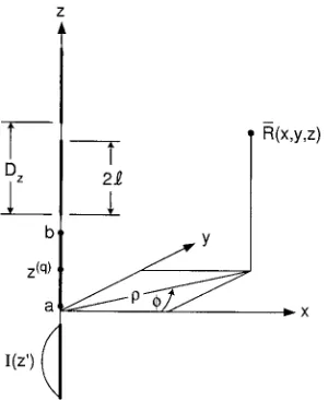
3.2 The Vector Potential and theH Field for Column Arrays of Hertzian Elements / 57
3.3 Case I: Longitudinal Elements / 59
3.3.1 Total Field from Infinite Column Array of z-Directed Elements of Arbitrary Length 2l / 60 3.3.2 The Voltage Induced in an Element by an
External Field / 61
3.3.3 The Mutual ImpedanceZq′,q Between a Column Arrayq and an External Elementq′ / 62 3.4 Case II: Transverse Elements / 64
3.4.2 TheyComponent of Eq / 69 3.4.3 ThezComponent ofEq / 72 3.5 Discussion / 74
3.6 Determination of the Element Currents / 76 3.7 The Double Infinite Arrays with Arbitrary Element
Orientation / 77
3.7.1 How to Get Well-Behaved Expressions / 77 3.8 Conclusions / 81
Problems / 82
4 Surface Waves on Passive Surfaces of Finite Extent 84
4.1 Introduction / 84 4.2 Model / 85
4.3 The Infinite Array Case / 85
4.4 The Finite Array Case Excited by Generators / 89 4.5 The Element Currents on a Finite Array Excited by an
Incident Wave / 89
4.6 How the Surface Waves are Excited on a Finite Array / 90
4.7 How to Obtain the Actual Current Components / 93 4.8 The Bistatic Scattered Field from a Finite Array / 94 4.9 Parametric Study / 96
4.9.1 Variation of the Angle of Incidence / 96 4.9.2 Variation of the Array Size / 100 4.9.3 Variation of Frequency / 102 4.10 How to Control Surface Waves / 108 4.11 Fine Tuning the Load Resistors at a Single
Frequency / 108
4.12 Variation with Angle of Incidence / 111 4.13 The Bistatic Scattered Field / 114 4.14 Previous Work / 115
4.16 Effects of Discontinuities in the Panels / 123 4.17 Scanning in theEPlane / 123
4.18 Effect of a Groundplane / 129
4.19 Common Misconceptions Concerning Element Currents on Finite Arrays / 130
4.19.1 On Element Currents on Finite Arrays / 130 4.19.2 On Surface Waves on Infinite Versus Finite
Arrays / 132
4.19.3 What! Radiation from Surface Waves? / 133 4.20 Conclusion / 133
Problems / 134
5 Finite Active Arrays 136
5.1 Introduction / 136
5.2 Modeling of a Finite ×Infinite Groundplane / 137 5.3 Finite×Infinite Array With an FSS Groundplane / 138 5.4 Micromanagement of the Backscattered Field / 140 5.5 The Model for Studying Surface Waves / 146 5.6 Controlling Surface Waves on Finite FSS
Groundplanes / 147
5.7 Controlling Surface Waves on Finite Arrays of Active Elements With FSS Groundplane / 148
5.7.1 Low Test FrequencyfL=5.7 GHz / 149 5.7.2 Middle Test FrequencyfM=7.8 GHz / 154 5.7.3 High Test FrequencyfH =10 GHz / 156 5.8 The Backscattered Fields from the Triads in a Large
Array / 158
5.9 On the Bistatic Scattered Field from a Large Array / 165 5.10 Further Reduction: Broadband Matching / 172
5.11 Common Misconceptions / 175
5.11.2 Can the RCS be Reduced by Treating the Dipole Tips? / 177
5.12 Conclusion / 178 Problems / 180
6 Broadband Wire Arrays 181
6.1 Introduction / 181
6.2 The Equivalent Circuit / 182
6.3 An Array With Groundplane and no Dielectric / 183 6.4 Practical Layouts of Closely Spaced Dipole Arrays / 184 6.5 Combination of the Impedance Components / 186 6.6 How to Obtain Greater Bandwidth / 187
6.7 Array with a Groundplane and a Single Dielectric Slab / 189
6.8 Actual Calculated Case: Array with Groundplane and Single Dielectric Slab / 191
6.9 Array with Groundplane and Two Dielectric Slabs / 193 6.10 Comparison Between the Single- and Double-Slab
Array / 195
6.11 Calculated Scan Impedance for Array with Groundplane and Two Dielectric Slabs / 195
6.12 Common Misconceptions / 198 6.12.1 Design Philosophy / 198
6.12.2 On the Controversy Concerning Short Dipoles / 202
6.12.3 Avoid Complexities / 205
6.12.4 What Is So Special Aboutλ/4 Anyway? / 207 6.12.5 Would a Magnetic Groundplane Be Preferable to
an Electric One (If It Were Available)? / 209 6.12.6 Will the Bandwidth Increase or Decrease When a
Groundplane Is Added to an Array? / 211 6.13 Conclusions / 211
7 An Omnidirectional Antenna with Low RCS 214
7.2 The Concept / 214
7.3 How do We Feed the Elements? / 216
7.4 Calculated Scattering Pattern for Omnidirectional Antenna with Low RCS / 217
7.5 Measured Backscatter from a Low RCS Omnidirectional Antenna / 217
7.6 Common Misconceptions / 221
7.6.1 On the Differences and Similarities of the Radiation Pattern / 221
7.6.2 How You Can Lock Yourself into the Wrong Box / 222
7.7 Conclusions and Recommendations / 223
8 The RCS of Two-Dimensional Parabolic Antennas 224
8.1 The Major Scattering Components / 224 8.1.1 The Reflector Scattering / 224
8.1.2 Total Scattering from a Parabolic Reflector with a Typical Feed / 226
8.2 Total Scattering from a Parabolic Reflector with Low RCS Feed / 228
8.2.1 The Bistatic Scattered Field as a Function of Angle of Incidence / 228
8.2.2 The Bistatic Scattered Field as a Function of Frequency / 230
8.3 Practical Execution of the Low RCS Feed / 232 8.4 Out-Of-Band Reduction / 233
8.5 Common Misconceptions on Edge Currents / 239 8.6 Conclusion / 240
9 Aperiodicity: Is It a Good Idea? 242
9.1 Introduction / 242
9.2 General Analysis of Periodic Structures with Perturbation of Element Loads and/or Interelement Spacings / 244
9.3 Perturbation of Arrays of Tripoles / 249 9.4 Making Use of Our Observations / 250
9.4.1 Multiband Designs / 252
9.4.2 The Original “Snowflake” Element / 254 9.4.3 The Modified “Snowflake” Element / 254 9.4.4 Elements with Mode Suppressors / 256 9.4.5 Alternative Design / 258
9.5 Anomalies due to Insufficient Number of Modes (The Unnamed Anomaly) / 258
9.6 Tapered Periodic Surfaces / 261 9.6.1 Introduction / 261
9.6.2 Physical Description / 262
9.6.3 Purpose and Operational Description / 263 9.6.4 Application of TPS to a Pyramidal Horn
Antenna / 266 9.6.5 Conclusions / 266 9.7 Conclusions / 267
10 Summary and Final Remarks 269
10.1 Summary / 269
10.1.1 Broadband Arrays / 269
10.1.2 On Antenna RCS and Edge Effect / 271 10.1.3 Surface Waves: Types I and II / 272
10.1.4 On Broadband Matching (Appendix B) / 274 10.1.5 A Broadband Meanderline Polarizer
(Appendix C) / 275
10.1.6 Aperiodic and Multiresonant Structures (Chapter 9) / 275
10.1.7 The Theory / 275
10.2 Are We going in the Right Direction? / 276 10.3 Let Us Make Up! / 278
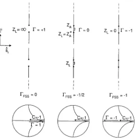
Appendix A Determination of Transformation and Position
Circles 281
A.1 Introduction / 281
Case I Given Load ImpedanceZL and Characteristic ImpedanceZ1 / 282
Case II BothZL and Z1 Located on the
Real Axis / 283
Case III Load ImpedanceZL Anywhere in the Complex Plane. Characteristic ImpedanceZ1 on the Real
Axis / 284
Case IV Two Arbitrary PointsB2 andB3 on
the Locus Circle forZin / 285 A.3 Where is Zin Located on the Transformation
Circle? Determination of the Position Circles / 286
Problems / 286
Appendix B Broadband Matching 288
B.1 Introduction / 288 B.2 Matching Tools / 289
B.3 Example: The Single Series Stub Tuner (Not Recommended for Broadband
Applications) / 293
B.4 Example: Broadband Matching / 295 B.5 The “TRICKS” / 296
B.6 Discussion / 297
B.6.1 Overcompensation / 297 B.6.2 How to Correct for
Undercompensation / 299 B.6.3 Alternative Approaches / 299 B.7 On the Load ImpedanceZL / 300 B.8 Example of a Practical Execution / 302 B.9 Common Misconceptions / 303
B.9.1 Should One Always Conjugate Match? / 303
B.9.2 Can New Exotic Materials Be Churned Out by Running Backwards? / 304 B.10 Concluding Remarks / 305
Appendix C Meander-Line Polarizers for Oblique Incidence 306
C.1 Introduction / 306
C.2 Multilayered Meander-Line Polarizers / 308 C.3 Individual Meander-Line Impedances / 310 C.4 Design 1 / 310
C.5 Design 2 / 315 C.6 Design 3 / 316 C.7 Design 4 / 316 C.8 Design 5 / 322 C.9 Conclusion / 326
Problems / 326
Appendix D On the Scan Versus the Embedded Impedance 327
D.1 Introduction / 327
D.2 The Scan Impedance / 328
D.3 The Embedded Stick Impedance / 330 D.3.1 Example / 333
D.4 The Embedded Element Stick Impedance / 333
D.5 On The Scan Impedance of a Finite Array / 335
D.6 How to Measure The Scan Impedance ZA / 340
D.7 Conclusions / 343 D.8 Postscript / 344
References 346
Foreword
It has often been said that a good teacher must have a number of attributes, among which are true expertise in the subject to be taught, and, just as important, the ability to put the subject across to the students, regardless of its complexity. We have all suffered under instructors who got straight A’s as students, but who never understood how their own students did not do as well because the material was presented as if it should be obvious. Professor Ben Munk has no problems in either regard.
In this book, Ben treats a number of subjects related to antennas and both their intended usage as transmission or reception devices, as well as the important (these days) radar cross section (RCS) that they can contribute. A constant theme behind the presented results is how often investigators approach the problem with no apparent understanding of the real-world factors that bear heavily on the practicality and/or quality of the result. He takes issue with those who have become so enchanted with high-powered computers that they simply feed the machine some wonderful equations and sit back while it massages these and “optimizes” a result. Sad to say, Ben has been able to document all too many examples to prove his point.
All this is not intended in any way to say that powerful computers are useless. Far from it. Without the use of such machines, much of the work described herein could not have been done in a lifetime, but the approach has to be controlled by investigators who understand the physics and electromagnetic realities that make a solution truly optimal and practical.
theory approach, combined appropriately with the detailed “method of moments,” produced successful solutions to a number of critical problems.
Here he further applies this approach and gives many examples of problems solved by himself and his graduate associates, with the goal of teaching by practical example. This is done by walking the reader, case by case, through the basic technology that applies, then to a logical solution. He then gives hard results to validate what was done, and then, to quickly bring the reader up to speed, he provides a problem or two for solution without further guidance.
Throughout all this, Ben uses his wonderful sense of humor to make various points, which goes a long way in making this book anything but tedious. Say-ing that about a book on heavy electromagnetic theory and design is certainly a far cry from the usual. His sections on “Common Misconceptions” are his way of highlighting how often “results” are developed and publicized without the necessary understanding of the basic rules of the game. He calls a spade a spade, for sure, and there may well be some who, though unnamed, might feel a twinge after reading these sections. All in all, this is an excellent book that will certainly benefit any serious investigator in the technology areas it discusses. Highly recommended!
WILLIAMF. BAHRET
Mr. W. Bahret was with the United States Air Force but is now retired. From the early 1950s he sponsored numerous projects concerning radar cross section of airborne platforms—in particular, antennas and absorbers. Under his leader-ship grew many of the concepts used extensively today—for example, the metallic radome. In fact he is considered by many to be the father of stealth technology.
BENMUNK
Wow!! The former student (now a professor emeritus) has succeeded in advanc-ing the former teacher’s (an even older professor emeritus) knowledge of array design tremendously.
The information contained in this book is going to change the way that large, broadbanded arrays are designed. This also leads to new insights in the area of antenna scattering. I strongly recommend it to the designers of such arrays. The concept of starting a finite array design from an infinite array is a remarkable one. A simple example of why I make this comment comes to mind. I was reading the papers in the December 2002IEEE Magazine which discuss the transmission of power to earth from space. Several problems with interference created by reradiation of energy at harmonic frequencies were discussed. I could see potential cures simply from scanning the initial chapters. I would also be interested in applying these concepts to my current research namely, time-domain ground-penetrating radar (GPR). Some neat antennas may become practical.
project supervisor, and later co-worker on much of that material. In reading it, I would turn pages and simply agree with many of the concepts.
At this time I have only scanned some of the chapters of the present book. For what I have seen thus far, I would scan a part of it and simply say, “Wow.” The reader should understand that there were points where I would have said, “Bet a Coke” (Ben and I used to bet a Coke every time we disagreed. Neither of us ever paid up.). These points are provocative to those readers with an interest in antenna scattering and should make those readers think carefully about them but most of them are resolved when one recalls that the emphasis of this book is on arrays.
This book is a must for anyone involved in the design of large arrays. I fully intend to read it very carefully after it is published.
Finally, I would observe that Ben’s comments about the review of journal papers are borne out of frustration. While Ben has worked in these areas through-out his career, most of his work was at that time classified. Thus when a paper in these general areas was published, he saw various flaws because of his expe-rience but he could not comment. Neither the paper’s author nor the reviewers, not having Ben’s unique background, would see these flaws. The problem is in reality created by the necessity of security. This same factor has led to the very interesting sections he has titled “Common Misconceptions.”
Columbus, Ohio LEONPETERS, JR.
Leon Peters, Jr., was a professor at the Ohio State University but is now retired. From the early 1960s he worked on, among many other things, RCS problems involving antennas and absorbers. In fact, he became my supervisor when I joined the group in the mid-1960s.
Preface
Why did I write this book?
The approach to engineering design has changed considerably over the last decades.
Earlier, it was of utmost importance to first gain insight into the physics of the problem. You would then try to express the problem in mathematical form. The beauty here was, of course, that it then often was quite simple to determine the location of the extreme values such as the maxima and minima as well as nulls and asymptotic behavior. You would then, in many cases, be able to observe which parameters were pertinent to your problem and in particular which were not. It was then followed by actual calculations and eventually by a meaningful parametric study that took into account what was already observed earlier.
The problem with this approach was, of course, that it required engineers and scientists with considerable insight and extensive training (I deliberately did not say experience, although it helps). However, not everyone that started down this road would finish and not without a liberal dose of humiliation.
It is therefore quite understandable that when the purely numerical approaches appeared on the scene, they soon became quite popular. Most importantly, only a minimum of physical insight was required (or so it was thought). The computers would be so fast that they would be able to calculate all the pertinent cases. These would then be sorted out by using a more or less sophisticated optimiza-tion scheme, and the results would be presented on a silver platter completely untouched by the human mind.
because the computer has been directed to incorporate all kinds of parameters that are alien to this particular problem. Or lack of physical insight has prevented the operator from obtaining a meaningful parametric study—for example, in cases where a solution does not exist in the parametric space considered.
The author has watched this development with considerable concern for sev-eral years. One of his colleagues stated recently that a numerical solution to a somewhat complex problem of his could only be used to check out specific designs. An actual optimization was not possible because of the excessive com-puter time involved.
That almost sounds like an echo of other similar statements coming from the numerical camp.
A partial remedy for this calamity would be, of course, to give the students a better physical understanding. However, a fundamental problem here is that many professors today are themselves lacking in that discipline. The emphasis in the education of the younger generation is simply to write a computer program, run it, and call themselves engineers! The result is that many educators and students today simply are unaware of the most basic fundamentals in electromagnetics. Many of these shortcomings have been exposed at the end of each chapter of this book, in a section titled “Common Misconceptions.” Others are so blatantly naive that I am embarrassed to even discuss them. What is particularly disturbing is the fact that many pursue these erroneous ideas and tales for no other reason than when “all the others do it, it must be OK!”
Neither this book nor my earlier one, Frequency Selective Surfaces, Theory and Design, make any claims to having the answers to all problems. However, there are strong signals from the readers out there that they more and more appreciate the analytic approach based on physical understanding followed up by a mathematical analysis. It is hoped that this second book will be appreciated as well.
The author shared this preface with some of his friends in the computational camp. All basically agreed with his philosophy, although one of them found the language a bit harsh!
However, another informed him before reading this preface that design by optimization has lately taken a back seat as far as he was concerned. Today, he said, there is a trend toward understanding the underlying mathematics and physics of the problem.
Welcome to the camp of real engineering. As they say, “there is greater joy in Heaven over one sinner who makes penance than over ninety-nine just ones.”
Acknowledgments
As in my first book,Frequency Selective Surfaces, Theory and Design, three of my many mentors stand out: Mr. William Bahret, Professor Leon Peters, Jr., and Professor Robert Kouyoumjian. They were always ready with consultation and advice. That will not be forgotten.
Further support and interest in my work was shown by Dr. Brian Kent, Dr. Stephen Schneider, and Mr. Ed Utt from the U.S. Air Force. After com-pletion of the development of the Periodic Method of Moments, the PMM code, the Hybrid radome, low RCS antennas, and more, the funding from the Air Force shifted into more hardware-oriented programs. Fortunately, the U.S. Navy needed our help in designing very broadbanded bandstop panels. Ultimately, this work resulted in the discovery of surface waves unique to finite periodic structures, which are treated in great detail in this book. The help and advice from Mr. Jim Logan, Dr. John Meloling, and Dr. John Rockway is deeply appreciated.
However, the most discussed subject was the Broadband Array Concept. It was set in motion by two of the author’s oldest friends, namely Mr. William Croswell and Mr. Robert Taylor from the Harris Corporation. This relationship resulted in many innovative ideas as well as support. So did my cooperation with Mission Research (home of many of the author’s old students). My deep-felt thanks goes to all who participated in particular Errol English who wrote Section 9.6 about Tapered Periodic Surfaces, and Peter Munk who supplied Section 3.7 investigat-ing Periodic Surfaces with arbitrary oriented elements.
curves for numerous cases in this book. He is currently interviewing. Lucky is the company that “secures” him.
Deep-felt thanks also go to my many friends and colleagues at the OSU ElectroScience Lab who supported me —in particular to Prof. Robert Garbacz, who graciously reviewed Chapter 2 concerning the RCS of antennas.
Finally, I was very lucky to secure my old editorial team, namely, Mrs. Ann Dominek, who did the typing, and Mr. Jim Gibson, who did a great deal of the drawings. In spite of their leaving the laboratory, they both agreed to help me out. And a fine job they did. Thank you.
Symbols and Definitions
a horizontal distance between columnq and point
of observation R
a, a1 wire radius of elements
a side length of square elements
dA vector potential for double infinite array of
Hertzian elements
dAq vector potential of Hertzian elements located in
columnq
dAqm vector potential of a single Hertzian element
located in column q and rowm
bm−1 location of the front face of dielectric slabm in
dipole case
bm location of the back face of dielectric slab m in
dipole case
Cp equivalent shunt capacitance from the orthogonal
elements in a CA absorber
d diameter of circular plate element
dm thickness of dielectric slab in dipole case
DN determinant of admittance matrix for N
slot arrays
Dx interelement spacings in theX direction
Dz interelement spacings in theZ direction
e=[pˆ× ˆr]× ˆr =⊥n⊥eˆ +||n||eˆ
field vector for infinite array of Hertzian elements
Em(R) electric field atRin medium m
Eim(R) incident electric field atRin medium m
E(R)m reflected electric field ofRin medium m
f frequency
fg onset frequency of grating lobe
F(w) Fourier transform off(t), not necessarily a
func-n (x) Hankels function of the second kind, ordernand
argumentx
Iqm(l) current along element in columnq and rowm
k, n indices for the spectrum of plane, inhomogeneous
waves from an infinite array
l distance from a reference point to an arbitrary
point on the element
2l1 total element length
dl infinitesimal element length
l element length of Hertzian dipoles
m± =E× ˆnD± magnetic current density
M± total magnetic current in slots
ˆ
nD unit vector orthogonal to dielectric interface
pointing into the dielectric medium in question ⊥nˆm =
nD× ˆr
|nD× ˆr| unit vector(s) orthogonal to the planes of inci-dence or reradiation in mediumm
||nˆm =⊥nˆm×r unit vector(s) parallel to the planes of incidence or reradiation in medium m
n, n0, n1, n2, . . . integers
ˆ
p orientation vector for elements
ˆ
p(p) orientation vector for element sectionp
ˆ
pp,n orientation vector for element section p in array
n
P(p) scattering pattern function associated with
ele-ment sectionp
P(p)t transmitting pattern function associated with
ele-ment sectionp
Pm(p) scattering pattern function associated with
ele-ment sectionp in mediumm ⊥
orthogonal and parallel pattern components of scattering pattern in medium m
⊥
orthogonal and parallel pattern components of transmitting pattern in mediumm
Pn polynomial for a bandpass filter comprised of n
slot arrays
q, m the position of a single element in columnq and
rowm
direction vectors in mediumm of the plane wave spectrum from an infinite array
rρ=
t variable used in Poisson’s sum formula
⊥
||Tm orthogonal and parallel transformation functions
for single dielectric slab of thickness dm E
⊥ ||
Tm orthogonal and parallel transformation function
for the E field in a single dielectric slab of thicknessdm
H
⊥ ||
Tm orthogonal and parallel transformation function
for the H field in a single dielectric slab of thicknessdm
⊥ ||Tm−m
′ orthogonal and parallel generalized
transforma-tion functransforma-tion when going from one dielectric slab of thicknessdmto another of thicknessdm′,
both of which are located in a general strati-fied medium
T .C.±1 transmission coefficient at the rootsY1±, etc.
V1,′1
induced voltage in an external element with ref-erence point R(1
′)
caused by all the currents from an array with reference element at R(1) VDi(1′±) induced voltage in an external element with
ref-erence pointR(1
′)
caused by a direct wave only from the entire array modes ending in the±direction
VS(1±′) induced voltage in an external element with ref-erence pointR(1
′)
caused by a single bounded mode ending up in the ±direction
⊥
||Wm orthogonal and parallel components for the
Wron-skian for a single dielectric slab of thick-nessdm
⊥ ||W
e
m orthogonal and parallel components for the
effec-tive Wronskian for a single dielectric slab of thickness dm and located in a general strati-fied medium
Y intrinsic admittance
Y1±, Y2±, . . . roots of polynomial for bandpass filter
YA scan admittance as seen at the terminals of an
element in the array
YL load admittance at the terminals of the elements
Y0=
1 Z0
intrinsic admittance of free space
Ym=1/Zm intrinsic admittance of mediumm
Y1,2 array mutual admittance between array 1 and 2
Z intrinsic impedance
Z= a+bz
c+dz the dependent variable as a function of the inde-pendent variablez in a bilinear transformation
Z0=1/Y0 intrinsic impedance of free space
ZA=RA+j XA scan impedance as seen at the terminals of an element in the array
ZL load impedance at the terminals of the elements
Zm=1/Ym intrinsic impedance of mediumm
Zn,n′ array mutual impedance between a reference
ele-ment in arrayn and double infinite arrayn′ Zq,q′
column mutual impedance between a reference element in columnq and an infinite line array atq′
Zq,q′m mutual impedance between reference element in
columnq and elementm in columnq′
α angle between plane of incidence and the
xy plane βm=
2π λm
propagation constant in mediumm.
l total element length of Hertzian dipole
ε dielectric constant
εeff effective dielectric constant of a thin dielectric
slab as it affects the resonant frequency
εm dielectric constant in mediumm
εrm relative dielectric constant in mediumm
η angle of incidence from broadside
ηg angle of grating lobe direction from broadside
E
⊥ ||
Ŵm+ =E⊥ ||
Ŵm,m+1 orthogonal and parallel Fresnel reflection
coeffi-cient for the E field when incidence is from media m tom+1
Ŵm,m+1 orthogonal and parallel Fresnel reflection
coeffi-cient for the H field when incidence is from media m tom+1
m+1 orthogonal and parallel effective reflection
coef-ficient for the E field when incidence is form media m tom+1
m,m+1 orthogonal and parallel effective reflection
coef-ficient for the H field when incidence is from media m tom+1
λm wavelength in mediumm
µm permeability in mediumm
µrm relative permeability in mediumm
E
⊥ ||
τm+=E⊥ ||
τm,m+1 orthogonal and parallel Fresnel transmission
coefficient for the E field when incidence is from media m tom+1
τm,m+1 orthogonal and parallel Fresnel transmission
coefficient for the H field when incidence is from media m tom+1
τm,me +1 orthogonal and parallel effective transmission coefficient for the E field when incidence is from media m tom+1
τm,me +1 orthogonal and parallel effective transmission coefficient for the H field when incidence is from media m tom+1
ω=2πf angular frequency
ω1ω0 andω1 variables used in Poisson’s sum formula (not
1
Introduction
1.1 WHY CONSIDER FINITE ARRAYS?
The short answer to this question is, Because they are the only ones that really exist.
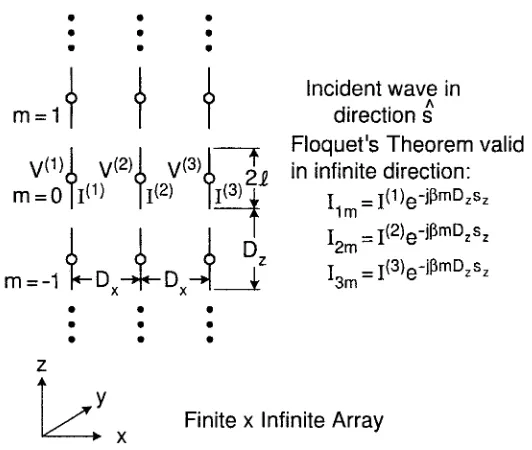
However, there are more profound reasons. Consider, for example, the infinite×infinite array shown in Fig. 1.1. It consists of straight elements of length 2l, and the interelement spacings are denotedDx andDz as shown. Such
an infinite periodic structure was investigated in great detail in my earlier book, Frequency Selective Surfaces, Theory and Design[1]. There the underlying theory and notation for the Periodic Moment Method (PMM) is described. It became the basis for the computer program PMM written by Dr. Lee Henderson as part of his doctoral dissertation in 1983 [2, 3].
In the intervening years it has stood its test and has become the standard in the industry.
Consider next the finite×infinite array shown in Fig. 1.2. It consists, like the infinite×infinite case in Fig. 1.1, of columns that are infinite in theZ direction, however, there is only a finite number of these columns in theX direction. Such arrays have been investigated by numerous researchers [4–23]—in particular, by Usoff, who wrote the computer program SPLAT (Scattering from a Periodic Linear Array of Thin wire elements) as part of his doctoral dissertation in 1993 [24, 25].
Let us now apply the PMM program to obtain the element currents for an infinite×infinite FSS array of dipoles withDx =0.9 cm andDz=1.6 cm, while
Finite Antenna Arrays and FSS, by Ben A. Munk
ISBN 0-471-27305-8 Copyright2003 John Wiley & Sons, Inc.
Fig. 1.1 An ‘‘infinite×infinite’’ truly periodic structure with interelement spacing Dx and Dz and element length 2l.
the element length 2l=1.5 cm; that is, the array will resonate around 10 GHz. The angle of incidence is 45◦ in the orthogonal plane (H plane). The current magnitudes are plotted column by column in Fig. 1.3a at f =10 GHz.
Similarly we apply the SPLAT program to obtain the current magnitudes in an finite×infinite array of 25 columns as depicted in Fig. 1.3b. We notice that the infinite case in Fig. 1.3a agrees pretty well with the finite case in Fig. 1.3b, except for the very ends of the finite array. This observation is typical in general for large arrays and is simply the basis for using the infinite array program to solve large finite array problems as encountered in practice. The deviation between the two cases (namely the departure from Floquet’s theorem [26] in the finite case) is usually of minor importance as long as the array is used as a frequency selective surface (FSS) like here [27]. However, if the array instead is designed to be an active array in front of a groundplane and each element is loaded with identical load resistors (representing the receiver or transmitter impedances), the situation may change dramatically. As shown in Chapters 2 and 5, we can in that case adjust the load impedances such that no reradiation takes place in the specular direction from all the elements except the edge elements. However, as also discussed in Chapter 5, we may change the loads for the edge elements such that no scattering in the specular direction takes place from these as well.
So far we have merely tacitly approved of the standard practice, namely the use of infinite array theory to solve finite periodic structure problems, at least in the case of an FSS with no loads and no groundplane. However, even in that case we may encounter a strong departure from the infinite array approach. In short, we may encounter phenomena that shows up only in a finite periodic structure and never in an infinite as will be discussed next.
1.2 SURFACE WAVES UNIQUE TO FINITE PERIODIC STRUCTURES
We have calculated the element currents only at f =10 GHz —that is, close to the resonant frequency of the array. Let us now explore the situation at a frequency approximately 25% lower, namely at f =7.8 GHz. From the SPLAT program we obtain the element currents shown in Fig. 1.3c, while the PMM program gives us element currents equal to 0.045 mA as shown in Fig. 1.3c, close to what would be expected based on the resonant value of 0.055 mA (see Fig. 1.3a).
We observe in Fig. 1.3c that the element currents for the finite array not only fluctuate dramatically from column to column but also exhibit an average current that can be estimated to be somewhat higher than the currents even for resonance condition (0.055 mA).
We shall investigate this phenomena in detail in Chapter 4. It will there be shown that the element currents are composed of three components:
2. Two surface waves, each of them propagating in opposite directions along the x axis. They will in general have different amplitudes but the same phase velocities that differ greatly from those of the Floquet currents. Thus, the surface waves and the Floquet currents will interfere with each other, resulting in strong variations of the current amplitudes as seen in Fig. 1.3c. 3. The so-called end currents. These are prevalent close to the edges of the finite array and are usually interpreted as reflections of the two surface waves as they arrive at the edges.
We emphasize that these surface waves are unique for finite arrays. They will not appear on an infinite array and will consequently not be printed out by, for example, the PMM program that deals strictly with infinite arrays. Nor should they be confused with what is sometimes referred to as edge waves [28]. The propagation constant of these equals that of free space, and they die out as you move away from the edges. See also Section 1.5.3.
Furthermore, the surface waves here are not related to the well-known sur-face waves that can exist on infinite arrays in a stratified medium next to the elements. These will readily show up in PMM calculations. These are simply grating lobes trapped in the stratified medium and will consequently show up only at higher frequencies, typically above resonance but not necessarily so in a poorly designed array. In contrast, the surface waves associated with finite arrays will typically show up below resonance (20–30%) and only if the interelement spacingDx is<0.5λ.
From a practical point of view, the question is of course whether these surface waves can hurt the performance of a periodic structure when used either passively as an FSS or actively as a phased array. And if so, what can be done about it.
We will discuss these matters next and in more detail in Chapters 4 and 5.
1.3 EFFECTS OF SURFACE WAVES
The most prevalent effects of the new type of surface waves associated with finite periodic structures depend to an extent upon whether they are used passively as an FSS or actively as a phased array.
In the first case we will observe a significant increase in the bistatic scattering. In the second case we will observe a variation of the terminal impedance as we move from column to column. Let us look upon these two phenomena separately.
1.3.1 Surface Wave Radiation from an FSS
Fig. 1.4 The bistatic scattered field in the H plane from a finite×infinite array of 25 columns at f=7.7 GHz. ( ) Scattering pattern calculated by using merely the Floquet currents—that is, simply by truncating an infinite structure. (– – –) Scattering pattern calculated by using the actual element currents (exact).
no perceptible change of the two main beams while the sidelobe level in this case is raised by about 10 dB (the exception is the sector between the two main beams where it actually is lower than the Floquet pattern). Later in Chapter 4 we will show more examples where the sidelobe level can be raised by more than 10 dB. In other words, the RCS of a finite FSS could be raised by that amount unless treated.
The encouraging conclusion is of course that even if the surface waves might actually be stronger than the Floquet currents (see, for example, Fig. 1.3c), they apparently radiate less efficiently than the Floquet currents. These facts will be discussed in detail in Chapter 4.
1.3.2 Variation of the Scan Impedance from Column to Column
If our periodic structure is fed as a phased array from constant voltage generators without generator impedances, the relative current magnitudes at the terminals will be like those shown in Fig. 1.3. Since the scan impedance is equal to the terminal voltage (namely the constant generator voltages) divided by the terminal currents, it is clear that the scan impedance will vary inversely to the currents in Figs. 1.3b and 1.3c.
Obviously it would be too much of a challenge to match an impedance with precision to the fluctuating scan impedance of Fig. 1.3c —in particular, when we realize that the maximum and minimum will start moving around with scan angle and frequency. Thus, we must simply look for ways to get rid of the surface waves or at least reduce them. We will discuss these matters next and in more detail in Chapter 4.
1.4 HOW DO WE CONTROL THE SURFACE WAVES?
1.4.1 Phased Array Case
In the previous section we considered phased arrays fed from constant voltage generators with the generator impedance equal to zero. We saw how this scenario could lead to disastrous variations in the scan impedance. Fortunately, a more realistic situation would be to feed the individual elements from constant voltage generators with generator impedances similar to the scan impedances as obtained from the infinite array case (i.e., approximating conjugate match). Thus, we show in Fig. 1.5a the same case as shown earlier in Fig. 1.3c but with load resistors equal to 100 ohms in order to simulate the generator impedances.
Several features are worth observing. First of all the fluctuations from element to element have been greatly reduced but obviously not completely eradicated. Second, the Floquet currents in Fig. 1.3c have been reduced from 0.045 mA to
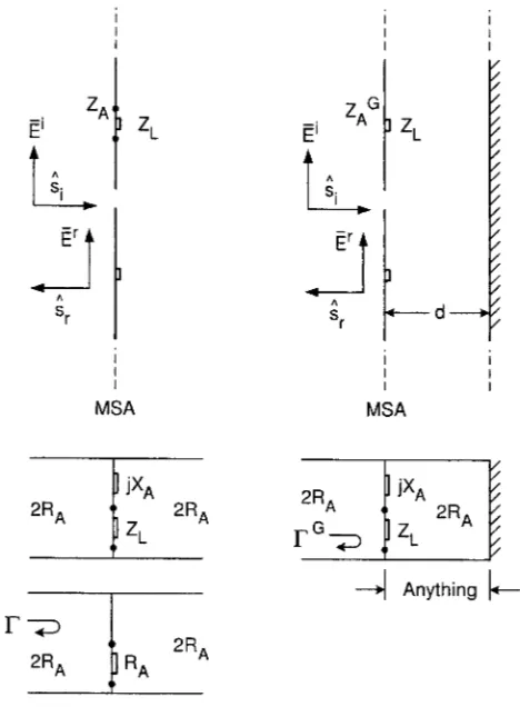
∼0.032 in Fig. 1.5a —that is, a reduction of approximately 0.032/0.045=0.71. This reduction is easy to explain by inspection of the equivalent circuit shown in Fig. 1.6a.
Fig. 1.6 The approximate equivalent circuit for an infinite periodic structure when used as: (a) A phased array with the individual elements fed from generators Vgwith generator impedances ZG. (b) A frequency selective surface when a voltage Viis induced by an incident wave and ZL is a load impedance (in general purely reactive).
without and with the generator impedance is seen to be ZA/(ZA+ZG). For the array considered here a rough estimate of the averageZA would be around 200 ohms. Thus, for ZG=100 ohms the reduction would be approximately 200/(200+100)=0.67, which is in fair engineering agreement with the observation above (namely 0.71).
We emphasize that this reduction is by no means “embarrassing.” It is in basic agreement with the conjugate matched case where the current ratio would be 0.50 and the efficiency 50%. See also the discussion in Appendix B.9.
But how do we explain the much stronger reduction of the ripples associated with the surface waves? Well, we shall later in Chapter 4 investigate surface waves in much more detail. It will there be shown that the terminal impedance associated with the surface waves is quite low, say of the order of Zsurf ∼ 10 ohms for each of the two surface waves. Thus, by the same reasoning as for the Floquet currents above, we find for each surface wave a reduction equal to 10/(10+100)=0.091. This is of course an average value but explains the strong ripple reduction observed in Fig. 1.5a.
This observation is quite noteworthy. It shows that by matching an antenna in the neighborhood of maximum power transfer (i.e., conjugate matching) we obtain an added benefit, namely a potential strong reduction of the ripples of the scan impedance even at a frequency where the surface waves are dominating.
Incidentally, the low value of the terminal surface impedance Zsurf is just another manifest of what has been observed earlier (see Fig. 1.4)—namely, that in spite of the fact that the surface wave currents may be stronger than the Floquet currents (see Fig. 1.3c), their radiation intensity will in general be considerably below that of the Floquet currents. Several actual calculated examples illustrating this statement will be given in Chapter 4.
1.4.2 The FSS Case
comparable to the terminal impedance ZA (about 3 dB). To gain further insight, let us consider the equivalent circuit for an FSS as shown in Fig. 1.6b. Here the generator voltages Vi are no longer produced by man-made generatorsVg but are instead induced by the incident plane wave. The objective at resonance is now simply to get as high a current as possible to flow through ZA and ZL in order to obtain lossless reflection from the surface. Thus, any load impedance
ZL should ideally be purely imaginary and serve merely to cancel any imaginary components ofZA.
So how do we control surface waves on an FSS?
One approach is to simply have no resistors anywhere over the entire surface, with the exception of a few columns at the edges. An example is shown in Fig. 1.5b, where the two outer columns have been loaded with 200 ohms, the next ones toward the center with 100 ohms, and finally the third column with 50 ohms. We observe a significant reduction of the ripple amplitudes as compared to the unloaded case in Fig. 1.3c. It should be noted that no parametric study was done on the resistive values of the loads at this point. More in Chapter 4.
We also show in Fig. 1.5c a case where each element over the entire surface has been loaded very lightly, namely with 20 ohms. We observe a strong reduction of the ripples from column to column—in particular, in the right half of the array. The transmission loss at resonance due to the 20-ohm load resistors is obtained from the equivalent circuit in Fig. 1.6b. The reduction of current is equal to
ZA/(ZA+ZL)=200/(200+20)=0.9, or about 1 dB (just barely permissible). Alternatively we may instead of the 20-ohm loss resistors obtain a moderate loss by simply using a slightly lossy dielectric next to the elements or simply a resistive sheet close to the elements.
Finally, many possibilities are open by combinations of the various approaches listed above. More about this in Chapter 4.
1.5 COMMON MISCONCEPTIONS
1.5.1 On Common Misconceptions
In my first book, Frequency Selective Surfaces, Theory and Design [1], I intro-duced at the end of each chapter a section called Common Misconceptions. It was intended to eradicate some of the many myths and misunderstandings that seem so prevalent “out there.” It was also intended to form the basis for further discussion in class. It soon became very popular. In fact, I became aware that these sections were often read with great glee before the text preceding them. This was manifested in well-meaning comments like: “Well, it is fine that you tell us what will and will not work. But you must also tell us why.” It slowly dawned on me that a new misconception had arrived: You just had to read the sections about common misconceptions and you would be up to speed and not make a fool out of yourself.
While I will admit to some parametric observations where no specific theo-retical background could be established right away, we are basically using an analytic approach1 that not only leads to a clear understanding of the problems but also establishes whether solutions exist and what they are.
I think it was Edison that once stated, “There is no substitute for hard work.”
1.5.2 On Radiation from Surface Waves
This title will undoubtedly raise a few eyebrows. As stated in many respectable textbooks, surface waves do not radiate —period. What is not always empha-sized is the fact that the theory for surface waves in general is based on a two-dimensional model like for example an infinitely long dielectric coated wire. And as discussed in this chapter infinite array theory may reveal many funda-mental properties about arrays in general but there are phenomena that occur only when the array is finite. The fact is that surfaces waves are associated with element currents. They will radiate on a finite structure in the same manner an antenna radiates, namely by adding the fields from each column in an end-fire array. Numerous examples of this kind of radiation pattern will be shown in Chapter 4. They are typically characterized by having a “mainbeam” in the direction of theXaxis that is lower than the “sidelobe” level. The reason for this “abnormality” is simply that the phase delay from column to column exceeds that of the Hansen–Woodyard condition by a considerable amount [29]. They also have a much lower radiation resistance.
An alternative approach is to assume that the radiation from a finite array is associated entirely with the edge currents. While Maxwell’s equations do not state specifically that radiation or scattering takes place from neither edges or element tips, it is nevertheless an observation that has proven valuable in classical electromagnetic theory. It is a convenient way to handle scattering properties from perfectly conducting half-planes, strips, wedges, and more, even when made of dielectric.
However, in the case of finite arrays of loaded wire elements the approach loses some of its appeal by the fact that surface waves exist only in a limited frequency range inside which the amplitude and phase vary considerably with frequency. Consequently, the scattering properties must be calculated numerically at each frequency and will actually also depend on array size in a somewhat complicated way.
At this point, this approach therefore is primarily of academic interest.
1.5.3 Should the Surface Waves Encountered Here Be Called Edge
Waves?
It has been suggested to denote the surface waves introduced in this chapter as “edge waves” for no reason other than they originate at the edges of the array. This confronts us with certain problems.
1By analytic we mean to separate a problem into components and study each of these individually
First of all, the term edge wave has been used to denote a wave that propagates along and not orthogonal to an edge [30]. In other words, we are talking about two entirely different kinds of waves.
Second, the term edge wave has been used by Ufimtsev and many others to denote waves that originate on the edges and propagate orthogonal to these all right [28]. However, that kind of edge wave dies down as you move away from the edge and their propagation constant is that of free space. The surface waves encountered here are basically not attenuated (except by radiation and ohmic losses) as they move away from the edge and propagate over the entire array.
Furthermore, the propagation constants of the waves encountered have been determined in Chapter 4 to be precisely equal to that of surface waves propagating along arrays of dipoles. These propagation constants are of course vastly different than that of free space. Thus, the surface waves encountered here should be called surface waves because that is what they are.
One is of course entitled to wonder why this phenomenon has gotten so sparse attention in the literature if any. The main reason is probably that the interelement spacing should be less than 0.5λand the frequency ∼20–30% below resonance (see Chapter 4 for details). Typically, many researchers choose a borderline spac-ing ofDx =0.5λand concentrate their attention around the resonance frequency [31–33]. As can be seen in Fig. 1.3, this basically precludes the existence of any strong surface waves.
1.6 CONCLUSION
We have demonstrated the presence of surface waves that can exist only on a finite periodic structure. It is quite different from the well-known types of surface waves that can exist in a stratified medium next to a periodic structure often referred to as Type 1. These merely represent grating lobes trapped inside the stratified medium. Thus, they will readily manifest themselves in computations based on infinite array theory at frequencies so high that grating lobes can be launched.
In contrast, the new type of surface wave (Type 2) can exist only if the interelement spacing Dx is so small that no grating lobe can exist. In addition, the frequency must typically be 20–30% below the resonance frequency of the periodic structure.
The presence of this new type of surface wave manifests itself in various ways:
1. If used as an FSS, it can lead to a significant increase in the bistatic scattering. In particular, we may observe a sizeable increase in the RCS of objects comprised of FSS without treatment.
We also indicated that this type of surface wave could be controlled in various ways. One approach is to load each element resistively. If used as an FSS, the resistors should have a low value in order not to significantly attenuate the reflected signal. In case of phased arrays a resistive loading could be obtained by simply feeding the elements from constant voltage generators with realistic generator impedances.
Alternatively, we could use no resistors at any of the elements across the surface but only at a few columns at the edges of the periodic structure. Slightly lossy dielectric slabs or even resistive sheets can also be used.
Finally, many possibilities are left open by combinations of some or all of the approaches above. See also Chapter 4 for details.
One might well ask the question, Why not just operate in a frequency range between the two types of surface waves? Well, in the case of an FSS it has been demonstrated numerous times that stability with angle of incidence can be obtained only for small interelement spacings (see, for example, reference 34). And basically the same is true for phased arrays in particular if designed for broad bandwidth. See Chapter 6 for details.
This introduction has merely pointed out the presence and treatment of surface waves that may exist below resonance for finite periodic structures. An in-depth investigation will be given in Chapter 4 where we will rely entirely on rigorously calculated examples.
PROBLEMS
1.1 Consider a phased array with scan impedance ZA=200 ohms. It is being fed from a generator with impedance ZG as shown in Fig. 1.6a. Assume conjugate match—that is, ZG=ZA=200 ohms.
As shown in Chapter 4, each of the two surface waves are generated from semi-infinite arrays located adjacent to the finite array. We will assume the equivalent circuit to consist of surface wave generators at each end of the finite array with surface wave generator impedances for the left- and right-going surface wave denotedZSWLandZSWR, respectively. We will assume that these impedances depend on angle of incidence.
Furthermore, we will assume that the generator impedancesZGare con-nected in series with ZSWL and ZSWR, separately; that is,ZG will reduce the surface waves as observed for example in Fig. 1.5a.
Given the surface wave impedancesZSWL andZSWRand the generator impedance ZG:
1. Find the reduction of the surface waves compared to the no-load case
ZG=0 forZG=200 ohms, in decibels forZSWL equal to
(d) 20.0 ohms (e) 40.0 ohms
2
On Radar Cross Section
of Antennas in General
2.1 INTRODUCTION
It is well known that the RCS of any antenna can be significantly reduced by placing a suitably shaped bandpass radome in front of it [35]. When the radome is opaque, the incident signal will primarily be reflected in the specular direction while the backscattered signal will be low as illustrated in Fig. 2.1. However, when the radome is transparent, no significant reduction of the antenna RCS will take place. Thus, the observable RCS will depend primarily on the antenna per se and whatever is behind the radome —for example, the back wall. It therefore becomes important to ask the scientifically very interesting question, “Is it pos-sible to design an antenna that basically is invipos-sible over a broad band in the backward sector without sacrificing its efficiency?”
Most readers will say no. They typically base their answer on well-documented facts about the most commonly used antennas such as a single dipole or monopole, the horn, the flat spiral, the corner reflector, the polyrod, the patch, the log peri-odic, the helical with a groundplane, and many more. These are all lacking in their ability to produce a low RCS over a broad frequency range when properly matched. Thus, we shall in this chapter instead concentrate on one of the few concepts that can truly produce invisibility in the backward sector, namely the large flat aperture in the form of an array backed by a groundplane and with uniform aperture illumination. The tapered case will also be discussed; and it will be shown that also in that case, invisibility is conceptually compatible with 100% efficiency.
Finite Antenna Arrays and FSS, by Ben A. Munk
ISBN 0-471-27305-8 Copyright2003 John Wiley & Sons, Inc.
Fig. 2.1 Use of a hybrid radome with bandpass characteristic to reduce the antenna RCS out of band.
A large flat aperture is most often associated with a narrow pencil beam. However, we shall in Chapter 7 consider antennas with omnidirectional pattern and low visibility in the backward direction over a broad band. Further discussed in Chapter 8 is how to design a feed for a parabolic cylinder that will produce an RCS about 6 dB lower than with no feed at all. The design of such a feed is closely related to the omnidirectional design. We emphasize, however, that parabolic systems never can attain the inherently low RCS level encountered for the flat aperture over a broad frequency band.
2.2 FUNDAMENTALS OF ANTENNA RCS
In this section we shall show that the field scattered (reradiated) from an antenna is comprised of two components:
1. Theantenna modecomponent depending on the gainG, the load imped-anceZL, the polarization, the angle of incidence and the frequency. 2. The residual mode component representing whatever must be added to
the antenna mode component to obtain the total RCS. It may or may not depend on the gain G, the polarization, the frequency, and the angle of incidence, but never on the load impedanceZL.
The definition of the residual mode admittedly violates a fundamental scientific principle: Never explain something unknown by something else unknown. Nev-ertheless, the concept is extremely useful for understanding antenna scattering.
Thus, we shall show several important examples where the residual scat-tering component is determined and illustrate how it relates to the antenna mode component.
An alternative and somewhat older nomenclature for the residual component is the structural scattering. We do not particularly recommend this nomenclature because it is somewhat misleading. For example, large arrays of dipoles without a groundplane will be shown later (see Section 2.6) to have as much residual scattering as antenna mode scattering. However, when we add a groundplane (yes, add more structure) the antenna mode is increased by a factor of four while the residual scattering simply as shown later is equal to zero. Thus, we avoid the word “structure” because it is burdened by the misconception that more structure means more scattering due to the structure. It may or it may not. See also Sections 2.14.1 and 2.14.2.
2.2.1 The Antenna Mode
More specifically, let us now consider an antenna exposed to an incident plane wave propagating in the direction sˆi and with power density i as shown in
Fig. 2.2. If the load impedanceZLis conjugate-matched to the antenna impedance
ZA, the received power is maximum and given by [36]
Preci = λ
2
4πGiipi, (2.1)
where Gi is the antenna gain in the direction of incidence sˆi and pi is the
polarization mismatch factor between the incident E-field and the polarization of the antenna, that is, 0≤pi ≤1.
We next seek the reflection coefficient Ŵ between the antenna impedance ZA and ZL. If one of them is real, the usual simple expression for Ŵ is valid
Fig. 2.2 An antenna with gain Gibeing exposed to an incident plane wave with power density
iand direction ˆsiwill receive the power Pirec=
λ2
4πGiipi, where pirepresent the polarization
mismatch between the antenna and the plane wave.
Fig. 2.3 How the reflection coefficient Ŵ between two complex impedance ZA=RA+jXA and ZL=RL+jXLis reduced to the simpler problem between the real impedance RAand the complex load RL+j(XA+XL).
must modify the original problem to the one shown in Fig. 2.3, bottom. This is based on the simple fact that for a two-port lossless circuit the magnitude (not the complex value) ofŴwill remain the same no matter where we place the terminals in the circuit. From the modified circuit the magnitude of the reflection coefficient between the real impedance RA and the complex impedanceRL+j (XL+XA)
is readily obtained as
|Ŵ| =
RL+j (XL+XA)−RA
RL+j (XL+XA)+RA
. (2.2)
The received power Prec given by (2.1) will be partly absorbed by the load
impedance ZL and partly reflected back toward the antenna as reflected power
given by
Prefl =Prec|Ŵ|2, (2.3)
Fig. 2.4 The power Precreceived by the antenna will be reradiated as Prefl=Prec|Ŵ|2. In the bistatic direction ˆsrthe antenna gain is Grand we obtain a power densityr=Prefl/4πr2Grpr, where pris the polarization mismatch between the antenna and a receiving antenna.
The reflected power Prefl will now be radiated (or rather reradiated) by the
antenna like any other signal impressed at its terminals.
If the antenna had been isotropic, the power Prefl would at a distance r be
uniformly distributed over a sphere with surface area 4π r2. Thus, the power density at distance r would be Prefl/4π r2. However, if the antenna has a gain
Gr in the direction of radiationsˆr as shown in Fig. 2.4, the power density in that
direction and at distancer will be
r =
Prefl
4π r2Grpr, (2.4)
wherepr is the polarization mismatch factor between the scattering antenna and
a receiving antenna located in the far field, that is, 0≤pr ≤1.
Substituting (2.1) and (2.3) in (2.4), we obtain
r =
λ2
16π2r2GiGrpipr|Ŵ| 2
i. (2.5)
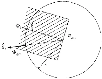
The definition of the radar cross section (RCS) is illustrated in Fig. 2.5. Here a fictitious flat plate, with areaσant, intercepts an incident plane wave with power
densityi—that is, the intercepted power is σanti.
If this power is spread uniformly in space at distance r, the power density ant is
The radar cross section of the antenna mode component is now defined as an areaσant so large that the power densityant associated with the fictitious plate is
the same as the power densityr associated with the antenna mode component;
that is, we set
Fig. 2.5 The power intercepted by a fictitious flat plate with area σant is σanti. When spread uniformly in space, it produces at distance r the power density ant=σanti/4πr2 orσant=4πr2ant/i. We defineσantsuch thatant=r—that is, equal to the power density
produced by the antenna. Thus, from earlier,σant=
λ2
4πGiGrpipr|Ŵ|
2.
Substituting (2.5) and (2.7) into (2.6) yields the radar cross section of the antenna mode:
σant=
λ2
4πGiGrpipr|Ŵ|
2. (2.8)
2.2.2 The Residual Mode
Expression (2.8) will in general not constitute the entire RCS of an antenna. In fact, it is only a component of the total radar cross section, which implies that there may be something else. This is usually called the residual (or structural) component σres. It was defined earlier as “whatever must be added to the field
associated withσant as given by (2.8) in order to obtain the field associated with
the total antenna RCS,” that is,
σtot ≡
λ2
4πGiGrpipr|Ŵ+C|
2 (2.9)
and the Residual scattering cross section is defined as
σres≡
λ2
4πGiGrpipr|C|
2. (2.10)
Note: σtot =σant+σres in general.
Inspection of (2.10) might seem to imply thatσresis proportional toGiGrpipr.
Fig. 2.6 Antenna mode:σant= λ 2 4πG
2
|Ŵ|2. Residual mode:σ res= λ
2 4πG
2
|C|2. Total antenna RCS:
σtot= λ 2 4πG
2
|Ŵ+C|2. All antenna RCS can be envisioned as made up of the antenna mode componentσantand the residual componentσres. The antenna mode component is proportional to|Ŵ|and can therefore be depicted in a Smith chart. The residual component represented by C can be larger thanŴ(top) or smaller (bottom).
it to σant to obtain σtot as given by (2.9). However, it does not depend on ZL. Otherwise it would have been part ofσant.
that case the tip of Ŵ will move along a circle with radius |Ŵ| ≤1 as shown in Fig. 2.6, top. We can in that way obtain a maximum σtot max as well as a minimum σtot min as shown. For conjugate match ZL =Z∗A and Ŵ=0; that is,
σtot is proportional to |C|2. Thus, for matching the load to maximum power transfer,σtot can be substantial if|C|is large; and what is worse, if|C|>|Ŵ|as is the case in Fig. 2.6, top, we can never obtain σtot =0 for any load.
2.3 HOW TO OBTAIN A LOWσtotBY CANCELLATION (NOT
RECOMMENDED)
We considered above the case where the residual component Cwas bigger than
Ŵ. We found thatσtot could never become zero no matter how we chose our load
impedance ZL. However, if we instead considered an antenna where|C|<1 as shown in Fig. 2.6, bottom (there are no particular limitations on C), we readily observe that we can choose the load impedanceZLsuch thatC+Ŵ=0; that is,
σtot min =0. This technique is referred to as RCS control by cancellation.
There are two strikes against this approach. First of all the load impedanceZL is not necessarily adjusted for conjugate match; that is, the power transfer is not perfect. But the biggest flaw is that the cancellation is in general very frequency-sensitive —that is, narrowbanded (ZLandZAwill in general change significantly and differently with frequency). And as if that is not enough, the cancellation condition changes in general with angle of incidence and polarization.
Therefore this approach should in general be discarded as being primarily of academic interest. See also Sections 2.14.1, 2.14.4, and 2.14.7, as well as Section 2.9 and Problem 2.2.
2.4 HOW DO WE OBTAIN LOWσtotOVER A BROAD BAND?
The answer to that question should by now be fairly obvious: Choose an antenna with a residual scattering close to zero (i.e.,C∼0) and keepŴas low as possible over as a broad a band as possible as illustrated in Fig. 2.7. That will ensure maximum power transfer (or almost) and lowσtot at the same time.
The reaction to this suggestion is typically something like: Well, we have measured dipoles, horns, parabolic dishes, flat spirals as well as helical antennas with groundplane, and what not, and we have never come across an antenna with no residual scattering. In fact we are not even sure whether an antenna without residual scattering violates certain fundamental rules!